


AN-881
One Technology Way • P. O . Box 9106 • Norwood, MA 02062-9106, U.S.A. • Tel : 781.329.4700 • Fax: 781.461.3113 • www.analog.com
APPLICATION NOTE
Flash/EE Memory Programming via LIN—Protocol 4
by Aude Richard
INTRODUCTION
A key feature of the ADuC7034 is the ability to download code
to on-chip Flash/EE memory while in-circuit. This in-circuit
code download is performed via the LIN communications bus.
This application note describes the download protocol implemented on the ADuC7034 (Protocol 4) to enable users to
develop their own LIN programming tools either for series
production programming or for application updates.
The term host refers to the host machine (microcontroller,
DSP, or other machine) attempting to download data to the
ADuC7034. The term loader refers specifically to serial
download firmware resident on the ADuC7034.
Note that this application note describes Protocol 4 only.
Protocol 6 is described in the AN-946 Application Note
Programming Flash/EE Memory via LIN—Protocol 6,
available from www.analog.com.
The protocol is shown on the part branding on Line 3
(see Table 1 ). A40 refers to a released version of Protocol 4
whereas A60 refers to a released version of Protocol 6.
Table 1. Branding Example
Line LFCSP
Line 1 ADuC7034
Line 2 BCPZ
Line 3 A40 #date code
Line 4 Assembly lot number
This protocol is LIN 2.0 compatible at 19.2 k baud, transmitting
8 bytes of data per packet. It is estimated that this protocol erases
and downloads 30,000 bytes to an ADuC7034 device in
approximately 35.9 secs.
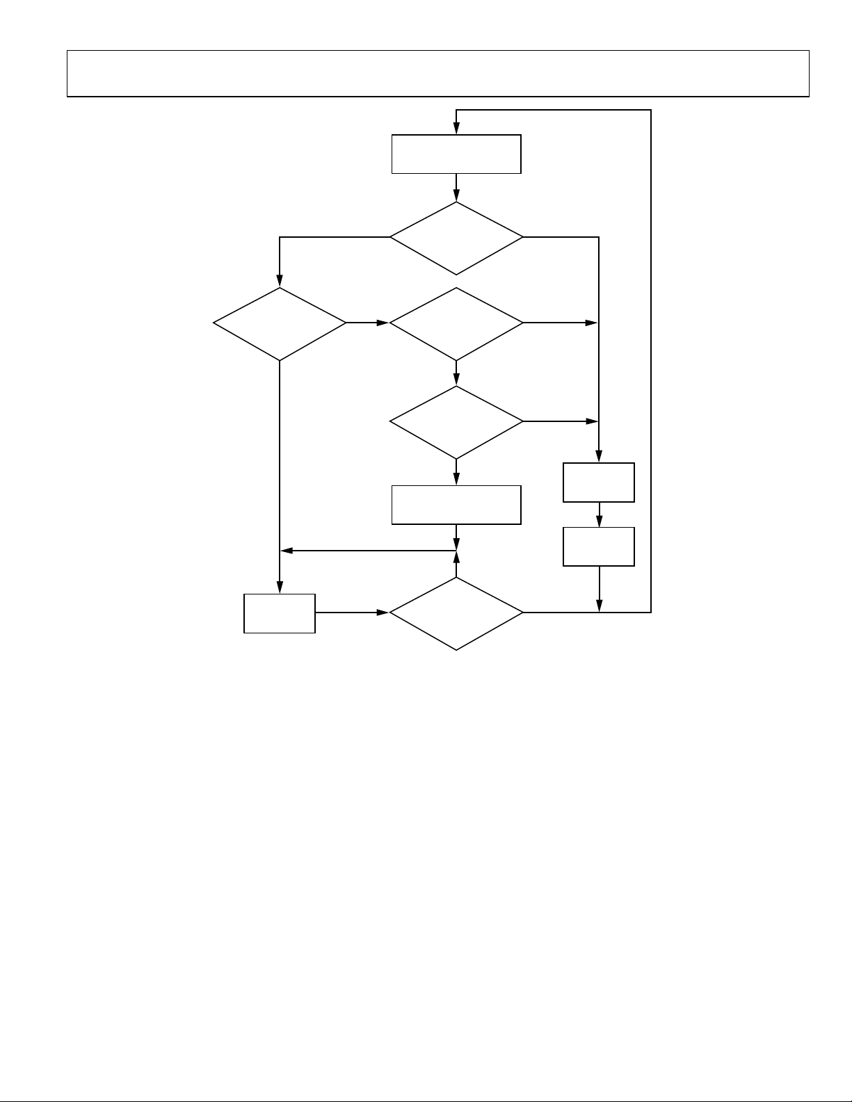
RUNNING THE ADuC7034 LOADER
To enable an unattended download via LIN, the ADuC7034
enters loader mode only if NTRST is low during reset and the
content of Flash/EE memory at Address 0x00080014 is not
0x27011970 or the Page 0 checksum, as illustrated in Figure 1.
Normally, NTRST is kept low and entry to download mode
is determined by the content of Flash Address 0x00080014.
Typically, in user applications, the value at Flash Address
0x00080014 is not 0xFFFFFFFF; therefore, user code must
have a built-in mechanism for corrupting Address 0x00080014
or erasing Page 0 (Flash Address 0x0 to Flash Address 0x200)
and for resetting the part. This mechanism allows entry to
download mode to reprogram the part. Ideally, the value at
Flash Address 0x00080014 should be programmed last to
enable re-entry to download mode in case the power fails or
another error occurs during reprogramming of the bulk of the
program.
The checksum of Page 0 is simply the sum of all the half words
in Page 0 excluding the two half words of the word at Address
0x00080014. This sum must be stored at Address 0x00080014.
Rev. 0 | Page 1 of 8

AN-881 Application Note
TABLE OF CONTENTS
Introduction ...................................................................................... 1
Running the ADuC7034 Loader..................................................... 1
User Code and System Code Requirements ............................. 4
Assigning PIDs via LIN ............................................................... 4
LIN Download Protocol Commands ........................................ 5
Secure Write Frames .................................................................... 5
Address Write Frames ...................................................................6
Verify Command Checksum Calculation ..................................6
Data Write Frame ..........................................................................7
Status Read Frame .........................................................................7
Additional Information ................................................................8
Rev. 0 | Page 2 of 8
Application Note AN-881
INITIALIZE ON-CHIP
PERIPHERALS TO FACTORY
CALIBRATED ST ATE
PAGE ERASED?
0x14 = 0xFFF FFFFF
YES
LIN COMMAND
NO YES
NO
NO
YES
JTAG MODE?
NTRST = 1
KEY PRESENT?
0x14 = 0x27011970
NO
CHECKSUM PRESENT?
0x14 = CHECKSUM
NO
FLAG PAGE 0 ERROR
NO
RESET
COMMAND
YES
YES
ERASE PAGE 0
SOFTWARE
RESET
Figure 1. Entering Download Mode
Rev. 0 | Page 3 of 8
06446-001

AN-881 Application Note
USER CODE AND SYSTEM CODE REQUIREMENTS
To enter download mode from user code, the user code must
change Address 0x00080014 so that it is neither 0x27011970 nor
the checksum. A reset must then be generated after which the
new code can be downloaded via LIN as per this standard.
In user code, use the following steps to perform a secure entry
sequence:
1. Enable Flash/EE erase and write commands (FEExMOD[3]).
2. Remove any protection on pages that are to be
reprogrammed, including at least Page 0.
3. Invalidate Address 0x00080014 by writing the value of
0x00000000 to Address 0x00080014.
4. Generate a reset.
5. The loader enters download mode.
6. Set the protected identifiers (PIDs) as described in the
Assigning PIDS via LIN section.
7. Send the L command to enable subsequent LIN download
commands.
8. Send the download commands and data to reprogram the
required pages. At this stage, Address 0x00080014 should
be given a value of 0xFFFFFFFF.
9. Verify all programmed pages. If an error is detected,
programming can be restarted from Step 4.
10. Program the checksum into Address 0x00080014.
11. Send the R command to cause a software reset.
12. The part enters user code.
In user code, it is important to ensure that this entire sequence
is not executed unintentionally.
This mechanism is dependent on the user code controlling
Address 0x00080014. If this is not implemented, the user is
not able to download via the LIN interface. It is still possible
to download via the JTAG interface because, upon reset,
NTRST is high (JTAG emulator is connected) and user
code is executed regardless of Address 0x00080014.
ASSIGNING PIDs VIA LIN
The ADuC7034 has PIDs assigned by default. To redefine these
PIDs the LIN diagnostic frame (0x3C) is used. The ADuC7034
does not reply to LIN diagnostic frames.
Use the following sequence to assign PIDs via LIN:
1. At the start of the download sequence, the loader checks all
frames for a PID of 0x3C. If the LIN frame does not contain
this diagnostic PID, then the LIN frame is ignored.
2. Once a LIN diagnostic frame with a PID of 0x3C is received,
the ADuC7034 device examines the LIN frame from Byte 0
to Byte 4. If they contain the NAD, PCI, SID, and supplier
ID as shown in Tab l e 2, the ADuC7034 device assigns the
message ID LSB in Byte 5 to the PID specified in Byte 7.
Table 2. LIN Diagnostic Frame
Byte Description Value
Byte 0 Node address (NAD) 0x7F
Byte 1
Byte 2 Service identifier (SID) 0xB1
Byte 3
Byte 4
Byte 5 Message ID, LSB 0x00/0x01/0x02/0x03
Byte 6 Message ID, MSB 0x00
Byte 7 User defined PID User value
Protocol control
information (PCI)
Analog Devices supplier
ID, LSB
Analog Devices supplier
ID, MSB
0x06
0x3A
0x00
3. The LIN master sends one to four of these packets,
containing the required user defined PIDs. Each PID
is associated with a message ID as shown in Table 3.
The secure write PID must be written and must be the
last LIN diagnostic frame written.
Table 3. Default PIDs
Message ID PID Default Frame ID
0x0000 Secure write 0xF0 0x30
0x0001 Address write 0xB1 0x31
0x0002 Data write 0x32 0x32
0x0003 Status read 0x73 0x33
4. The loader now recognizes only the L command using the
secure write PID.
5. After the L command is received, the R, E, W, and V com-
mands as well as data write and status read frames can be
sent using these four PIDs. Commands not using one of
these four PIDs are ignored.
The reassignment of the PIDs for address write, data write,
and status read is optional. Assigning the secure write frame
PID is not optional and must be the last PID assigned by a
diagnostic frame.
The diagnostic frame’s associated checksum is the classic
checksum, that is, the checksum is calculated only over the
data. All other packets use the enhanced checksum.
The parity bits constitute part of the PID.
Rev. 0 | Page 4 of 8

Application Note AN-881
LIN DOWNLOAD PROTOCOL COMMANDS
The ADuC7034 LIN download protocol contains five
commands (see Table 4 ).
Table 4.
Command Description
L
E This command is used to erase Flash/EE pages.
W
V
R
The five commands (shown in Tab l e 4) are split between four
PIDs as described in Ta b le 5 .
Table 5. LIN Diagnostic Frame
LIN Frame PID
Secure Write 0xF0 L
R Reset
Flash/EE
Address Write
W Write Flash/EE
V Verify
Flash/EE Data
Write
Status Read 0x73 User value Status read
For all commands associated with the Flash/EE address write
PID, the physical location of the memory, 0x00080000 to
0x000877FF, should be used as opposed to the mapped region,
0x00000000 to 0x000077FF. If the mapped address is used, the
command executed is not be successful.
All packets are 8 bytes in length and unused/reserved packets
contain 0xFF.
The secure write, Flash/EE address write, data write, and the
status read LIN frames have an enhanced checksum, that is,
the checksum is calculated over the data and PID.
This command is used to enter LIN download
mode. It is only used after the secure write PID is
assigned.
This command is used to write data to the
Flash/EE.
This command is used to generate a 32-bit
checksum over a specified range in Flash/EE.
This command is used to generate a software
reset. For more information on software resets,
refer to the ADuC7034 data sheet.
Default PID
Value
0xB1 E Erase Flash/EE
0x32 User value Data for Flash/EE
Valid
Command
Result of
Command
Enter LIN
download mode
SECURE WRITE FRAMES
L Command
The LIN enter download mode command puts the loader into
LIN download mode. This command is associated with the
secure write frame PID, as received in the diagnostic frame.
Syntax: <L[1] 0xFF[1] Key[1] 0xFF[5]>
For example, to enter download mode, use the following
command:
<L 0xFF 0x42 0xFF 0xFF 0xFF 0xFF 0xFF>
Key B (0x42) is required for the command to succeed.
Table 6. LIN Enter Download Mode Frame
Byte Description Value
Byte 0 Command L 0x4C
Byte 1 Reserved for future use 0xFF
Byte 2 LIN download entry key 0x42
Byte 3 Reserved for future use 0xFF
Byte 4 Reserved for future use 0xFF
Byte 5 Reserved for future use 0xFF
Byte 6 Reserved for future use 0xFF
Byte 7 Reserved for future use 0xFF
R Command
The reset command generates a software reset. For more
information on the implications of a software reset, refer
to the ADuC7034 data sheet.
Syntax: <R[1] 0xFF[1] Key[1] 0xFF[5]>
For example, to initiate a reset, use the following command:
<R 0xFF 0xBD 0xFF 0xFF 0xFF 0xFF 0xFF>
Table 7. LIN Reset Frame
Byte Description Value
Byte 0 Command R 0x52
Byte 1 Reserved for future use 0xFF
Byte 2 LIN download entry key 0xBD
Byte 3 Reserved for future use 0xFF
Byte 4 Reserved for future use 0xFF
Byte 5 Reserved for future use 0xFF
Byte 6 Reserved for future use 0xFF
Byte 7 Reserved for future use 0xFF
Rev. 0 | Page 5 of 8

AN-881 Application Note
ADDRESS WRITE FRAMES
E Command
The erase Flash/EE command erases pages of Flash/EE.
For a Flash/EE with 512 byte pages, the number of bytes
specified divided by 512 pages are erased. The number of
bytes should be a multiple of 512, otherwise the number of
pages is rounded down.
The erase command only responds to the PID for Flash/EE
address write.
Syntax: <E[1] address[4] number of bytes to erase[2] 0xFF[1]>
For example, to erase Page 0 and Page 1, use the following
command:
<E 0x00 0x00 0x08 0x00 0x00 0x04 0xFF>
Table 8. LIN Erase Flash/EE Frame
Byte Description Value
Byte 0 Command E 0x45
Byte 1 Start address, LSB N/A
Byte 2 Start address, second byte N/A
Byte 3 Start address, third byte N/A
Byte 4 Start address, MSB N/A
Byte 5 Number of byte LSB N/A
Byte 6 Number of byte MSB N/A
Byte 7 Reserved for future use 0xFF
W Command
The write Flash/EE command prepares writing data to an erased
page of Flash/EE. The number of bytes, defined in Byte 5 and
Byte 6, is written to Flash/EE, starting at the address specified
in Byte 1 to Byte 4.
The write command only responds to the PID for Flash/EE
address write.
Syntax: <W[1] Address[4] number of bytes to write[2] 0xFF[1]>
For example, to initiate a write command to the second page of
Flash/EE, use the following command:
<W 0x00 0x02 0x08 0x00 0x00 0x02 0xFF>
Table 9. LIN Write Flash/EE Frame
Byte Description Value
Byte 0 Command W 0x57
Byte 1 Start address, LSB User value
Byte 2 Start address, second byte User value
Byte 3 Start address, third byte User value
Byte 4 Start address, MSB User value
Byte 5 Number of byte LSB User value
Byte 6 Number of byte MSB User value
Byte 7 Reserved for future use 0xFF
This LIN write Flash/EE frame is then followed by data packets.
The data packets are associated with the data write PID for
Flash/EE data write.
It is recommended to program Page 0 last, excluding Address
0x00080014.
The number of bytes specified may not be more than 512. Data
packets of 8 bytes are transmitted.
After the W packet and all data packets are transmitted, a verify
command should be executed over the region written to. The
write procedure does not check the data as it is written.
V Command
The verify command causes the 32-bit sum of all the half
words of the selected pages to be calculated and put in the
status memory, which may be read back by a status read command. If a nonpage-aligned address or number of bytes to verify
is selected, this value is rounded down to the nearest page.
The verify command only responds to the PID for Flash/EE
address write.
Syntax: <V[1] Address[4] number of bytes to verify[2] 0xFF[1]>
For example, to generate a checksum of the second and third
pages (1024 bytes) of Flash/EE, use the following command:
<V 0x00 0x02 0x08 0x00 0x00 0x04 0xFF>
Table 10. LIN Verify Flash/EE Frame
Byte Description Value
Byte 0 Command V 0x56
Byte 1 Start address, LSB User value
Byte 2 Start address, second byte User value
Byte 3 Start address, third byte User value
Byte 4 Start address, MSB User value
Byte 5 Number of byte LSB User value
Byte 6 Number of byte MSB User value
Byte 7 Reserved for future use 0xFF
VERIFY COMMAND CHECKSUM CALCULATION
The verify command generates a 32-bit value, which represents
the sum of the 16-bit values from the start location, specified in
the V frame, over the number of bytes required.
BytesofNumber
−=
∑
LocationStart
For a single 512 byte page, 500 μs are required after the V packet is
received by the ADuC7034 device until the start of any subsequent LIN frames.
WordsBitChecksum 16
Rev. 0 | Page 6 of 8

Application Note AN-881
DATA WRITE FRAME
Data consists of one or more 8-byte LIN packets.
This data is written to Flash/EE as it is received. The number of
data packets transmitted is dependent on the number of bytes
specified in the preceding address write command. The number
of bytes specified is divided by eight to give the number of data
packets. Unused data bytes must be padded with 0xFF. These
padded bytes do not affect the Flash/EE.
Table 11. LIN Flash/EE Data Frame
Byte Description Value
Byte 0 Data 1 0x45
Byte 1 Data 2 User value
Byte 2 Data 3 User value
Byte 3 Data 4 User value
Byte 4 Data 5 User value
Byte 5 Data 6 User value
Byte 6 Data 7 User value
Byte 7 Data 8 0xFF
If any other PID is received before all required data packets are
completed, the data stream is terminated and a write error is
flagged.
After the data is written, it should be verified using the verify
command. This checksum can be read by a status read and
compared to the expected checksum by the master.
The following paragraphs list further information regarding the
bytes in Ta b le 1 1 :
• Byte 0 indicates the last command executed, that is, E, L,
W, o r V.
• Byte 1 indicates the device ID byte from Analog Devices, Inc.
0x34—ADuC7034
• Byte 2 contains good/bad status bit for last command
executed.
The relevant bit is cleared to indicate the command
completed successfully and set to indicate a failure. F
corresponds to the Flash Page 0 error flag.
<F 0 0 0 E 0 W V>
• Byte 3 is reserved for future use.
• Bytes 4 to Byte 7 give data depending on the last command
executed (verify).
No memory read command is given for user code protection and
download protocol efficiency.
Note that all values are transmitted in hexadecimal bytes
represented as two nibbles.
STATUS READ FRAME
When the master node of the LIN bus requests a read of the
slave node, the status frame is read. An 8-byte LIN packet is read
by status read.
Table 12. LIN Status Frame
Byte Description Values
Byte 0 Last command executed User value
Byte 1 Device ID byte 0x30/0x34
Byte 2
Byte 3 Reserved for future use 0xFF
Byte 4
Byte 5
Byte 6
Byte 7
Status for each command when last
executed
Checksum LSB for V command (reserved
otherwise)
Checksum second byte for V command
(reserved otherwise)
Checksum third byte for V command
(reserved otherwise)
Checksum MSB for V command
(reserved otherwise)
User value
User value
User value
User value
User value
Rev. 0 | Page 7 of 8

AN-881 Application Note
ADDITIONAL INFORMATION
Example
Tabl e 1 3 is an example sequence for downloading 512 bytes to Page 2. The example utilizes the ADuC7034.
Table 13. Example Sequence
PID Command1 Description
0x3C 0x7F 0x06 0xB1 0x3A 0x00 0x01 0x00 AW AW is the address write PID
0x3C 0x7F 0x06 0xB1 0x3A 0x00 0x02 0x00 DW DW is the data write PID
0x3C 0x7F 0x06 0xB1 0x3A 0x00 0x03 0x00 SR SR is the status read PID
0x3C 0x7F 0x06 0xB1 0x3A 0x00 0x00 0x00 SW SW is the secure write PID
SW L 0xFF 0x42 0xFF 0xFF 0xFF 0xFF 0xFF
AW E 0x00 0x02 0x08 0x00 0x00 0x02 0xFF
SR E 0x30 0x00 0xFF 0xFF 0xFF 0xFF 0xFF Good status
AW W 0x00 0x02 0x08 0x00 0x00 0x02 0xFF Write 512 bytes at Address 0x80200
DW Usercode
DW Usercode
…
…
DW Usercode Last packet to write
AW V 0x00 0x02 0x08 0x00 0x00 0x02 0xFF Generate checksum of second page
SR V 0x30 0x00 0xFF CS CS is the 4-byte checksum
… Program other pages
…
SW R 0xFF 0xBD 0xFF 0xFF 0xFF 0xFF 0xFF Generate a reset and run user code
1
The first three diagnostic frames are optional. If not sent, then the default values for AW, DW, and SR are used.
LIN Protocol Download Speed
According to LIN 2.0 protocol, each LIN frame has a slot equal
to, or longer than, the maximum frame size. Accordingly,
T
FRAME SLOT
= T
HEADER MAXIMUM
= 1.4 × (T
HEADER NOMINAL
= 1.4 × (34 × T
+ T
RESPONSE MAXIMUM
+ ( 10 × (N
BIT
+ T
RESPONSE NOMINAL
DATA
+ 1 ) × T
)
))
BIT
Sequence to enter download protocol
Key = B (0x42)
Erase the content of one page, starting from the second
page
Download data to Flash
64 packets required
For more information on LIN frame length refer to the LIN 2.0
specification, LIN Protocol Specification, Section 2.2 Frame Slots.
A single page erase takes 20 ms. To erase the entire 30 kB
user space takes 1.2 secs. Using Protocol 4, each frame slot is
9.04 ms. This is the time it takes to download 8 bytes. Therefore, programming the entire user space (30 kB) takes 34.7 ms.
©2008 Analog Devices, Inc. All rights reserved. Trademarks and
registered trademarks are the property of their respective owners.
AN06446-0-5/08(0)
Rev. 0 | Page 8 of 8
 Loading...