

AN-850
APPLICATION NOTE
One Technology Way • P.O. Box 9106 • Norwood, MA 02062-9106, U.S.A. • Tel: 781.329.4700 • Fax: 781.461.3113 • www.analog.com
Adaptive Digital Line Length Tracking
by Frank Kearney
INTRODUCTION NOISE-INDUCED TIME-BASE INACCURACIES
Despite the rapid advancement of digital TV, analog TV
remains dominant for both transmission and display. Analog
video formats, like digital formats, have precise specifications
for how to format video. These specifications include how the
luma, chroma, and synchronization information is packaged to
provide the line, field, and frames of video information that
recreate the images observed on TV screens. To display the
video information accurately, each of these components must be
correctly extracted from the video signal. Similarly, the timing
and phase information must be maintained or recreated as it
was when the video signal was first encoded at the source.
This application note outlines the challenges encountered when
decoding and restoring a correct time base to nonstandard
input video sources. This technology is known as Adaptive
Digital Line Length Tracking (ADLLT™).
Video signals consist of various components, some of which can
be altered or corrupted within the transmission path, resulting
in distortion of some video package aspects. For RF transmitted
signals, the synchronization information is normally present on
the recovered signal, but its detection and extraction can be
difficult or impossible because of excessive noise. It is important
to note that even when recovering the synchronization is
possible, its detection can be offset due to noise, which in turn
introduces jitter on the recovered synchronization information.
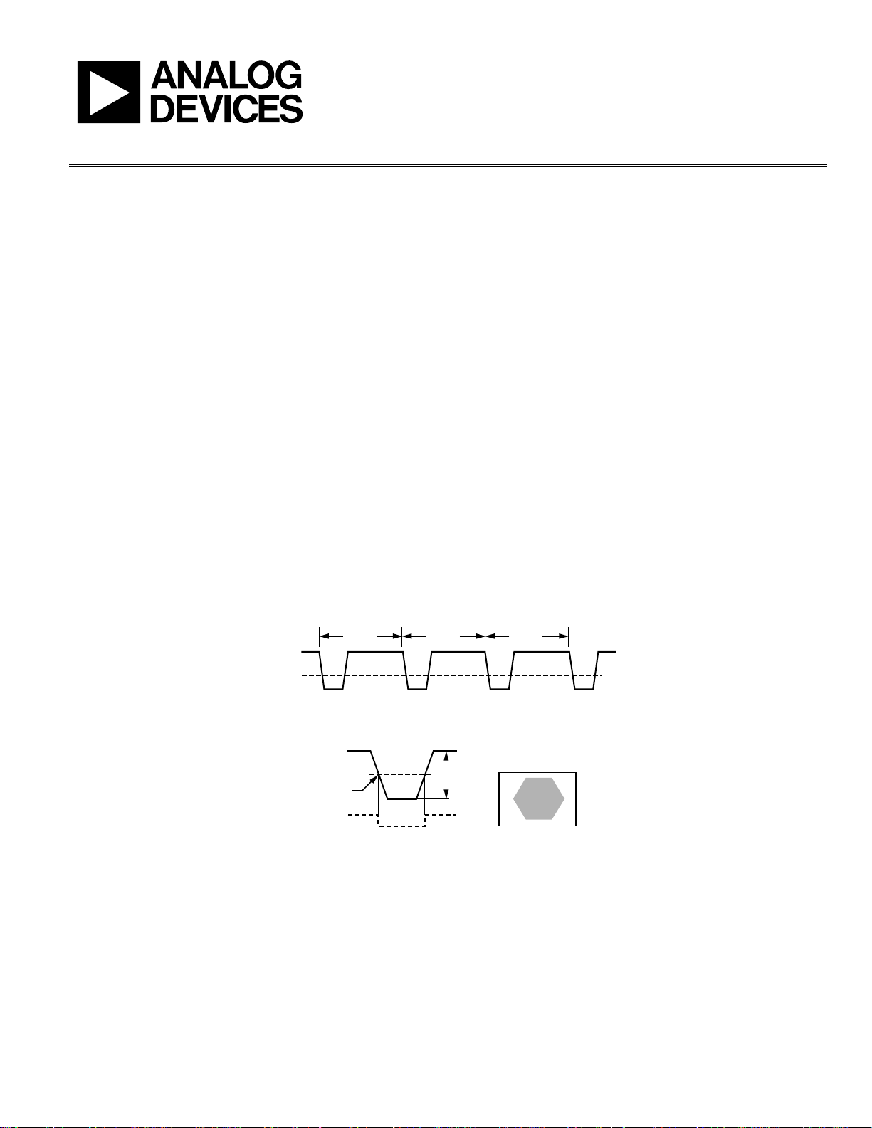
Figure 1 shows a representation of a typical stream of line
synchronization information.
Figure 2 shows that slicing the
synchronization information from this stream results in a stable
video display.
≈ 64µs≈ 64µs≈ 64µs
SYNC
SLICE
LEVEL
Figure 1. Line Synchronization Stream Without Noise at Source
06143-001
SLICE
50% TIMING
SLICED HSYNC
Figure 2. Stable Synchronization Extraction with No Vertical Jitter on Displayed Image
BLANK
LEVEL
PICTURE HAS STABL E
VERTICAL EDGES
6143-002
Rev. 0 | Page 1 of 8

AN-850
TABLE OF CONTENTS
Introduction ...................................................................................... 1
VCR-Induced Time-Base Errors .................................................5
Noise-Induced Time-Base Inaccuracies........................................ 1
Revision History ............................................................................... 2
REVISION HISTORY
7/06—Revision 0: Initial Version
ADLLT............................................................................................6 T
Rev. 0 | Page 2 of 8
AN-850
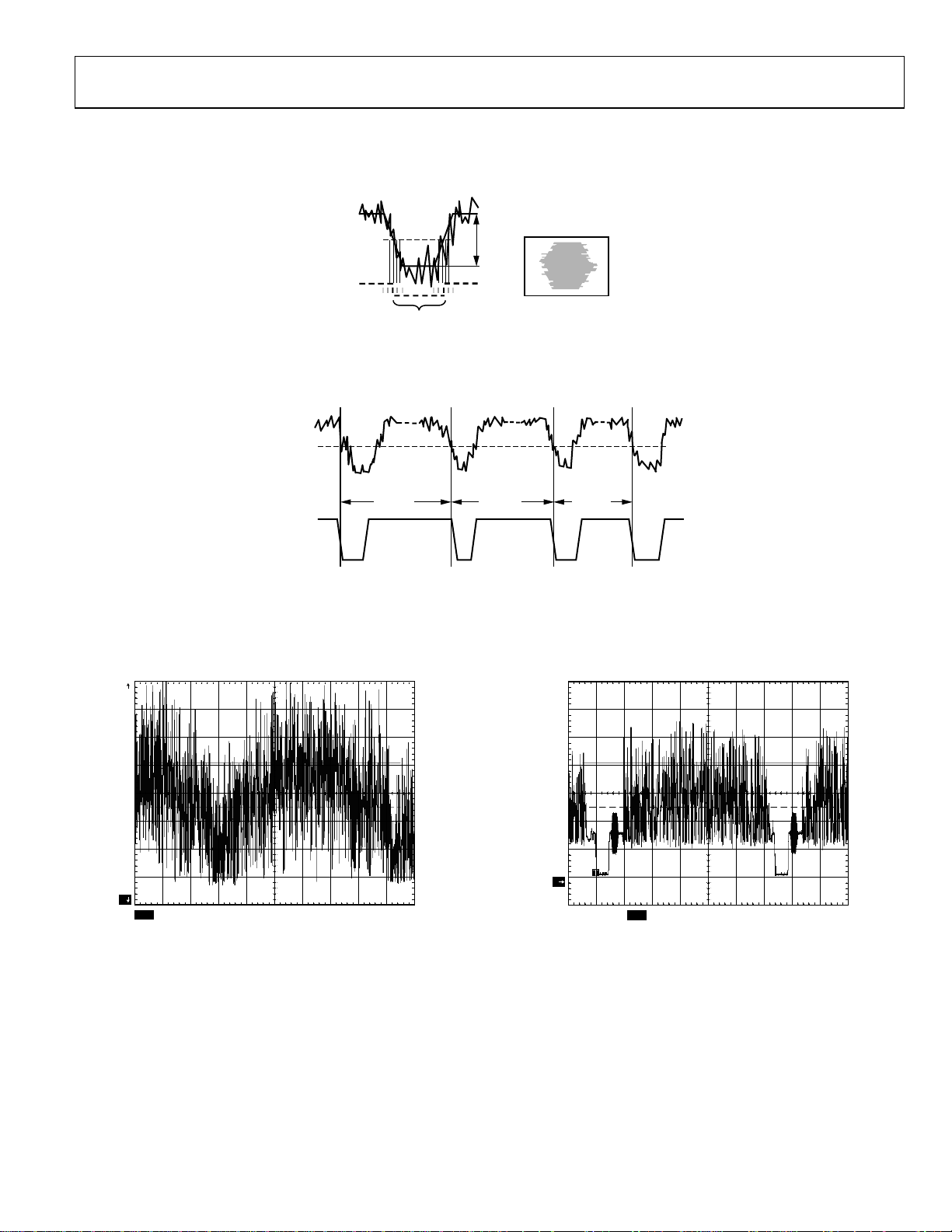
Figure 3 is a representation of how noise can distort the synchronization information, resulting in a misinterpretation of the synchroniza-
Figure 3 shows the resulting stripped synchronization that can result from the noise. Note that the time base is corrupted and jitter
tion.
introduced. The effect of this jitter on the displayed video is serrations at the start and end of each line (see
SLICE
VISIBLE JITTER ON
50% POINTS
CORRUPTED
BY NOISE
VERTICAL EDG ES
06143-004
Figure 3. Noisy Synchronization Information Resulting in Extracted Synchronization Jitter
SYNC
SLICE
LEVEL
≈ 63µs≈ 64µs≈ 65µs
Figure 4).
Figure 4. HSYNC Jitter Resulting in Line-to-Line Shifting of Displayed Image
A typical noisy input from a tuner source is shown in
information.
Figure 6 illustrates the decoder output re-encoded into an analog format.
2
1
CH1 200mV CH2 200mV M10µs VID CH2 Ο/110
Figure 5. Actual Video Output from Tuner Source
Measured on Input to Decoder
Figure 5
6143-005
06143-003
. It demonstrates the difficulty in determining the synchronization
2
CH2 200mV M10µs VID CH2 Ο/110
Figure 6. Decoder Output with Correct Noise-Free Synchronization Restored
06143-006
Rev. 0 | Page 3 of 8

AN-850
The introduction of noise is a common issue for video that has come through a transmission path. It is also common for components of
the video signal to be attenuated or amplified, resulting in nonlinear characteristics in the video package. An example of a video signal
seen at the input to the ADV decoder is shown in
other components of the video signal remain at the proper amplitudes. The restored synchronization information, along with the other
signal components that maintain their correct levels, is seen in
1
Figure 7. The synchronization level is reduced close to the blanking level, while the
Figure 8.
2
CH1 200mV M10µs VID CH2 Ο/110
Figure 7. Input Video Signal with Attenuated Synchronization
06143-007
Figure 8. Output Video Signal with Correct Synchronization Level Restored
M10µs VID CH2 Ο/110CH2 200mV
6143-008
Rev. 0 | Page 4 of 8

AN-850
VCR-INDUCED TIME-BASE ERRORS
Unlike common transmission path induced errors where
synchronization is normally present but can be distorted, video
from VCR sources can have missing or incorrect synchronization
information. VCRs are essentially mechanical devices. Variance
in mechanics such as motor speed, belt wear, and head
switching can introduce time-base corruption. In the case of
head switching and VCR trick modes, time base is not only
corrupted, but can also be lost (see
switching occurs, all video and synchronization is lost. The
result is a flat dc output for this duration.
3500
3000
2500
2000
1500
AMPLITUDE
1000
Figure 9). When head
06143-010
Figure 10. Output Image with Top Curl
The ADLLT technology of ADV decoders results in the correct
restoration of the time base. The top curl, PLL lock in artifact is
eliminated (see
Figure 11).
500
0
07
123456
TIME
Figure 9. VCR Missing Signal During Head Switch
Such time-base errors normally result in lock in errors in the
downstream HSYNC PLL and give rise to an artifact on the
output image known as top curl (see
Figure 10).
06143-009
06143-011
Figure 11. Output Image with Top Curl Eliminated
Rev. 0 | Page 5 of 8

AN-850
R
R
ADLLT
ADLLT incorporates the functionality of Analog Devices, Inc.
(ADI) synchronous detection and extraction blocks, resampler,
and advanced back end FIFO management.
ADI advanced digital video decoders filter the window in which
they look to detect synchronization. In addition, the decoders
use PLL blocks with HSYNC and VSYNC processor blocks to
ensure that the synchronization information is correctly
extracted. The filters ensure that the decoder gates the time in
which it looks for synchronization information. Previously,
excessive noise outside of this region would have dipped below
the slice level and been seen as synchronization. This noise is
now ignored. The synchronization PLL and processor blocks
ensure that synchronization detected within the gated period is
correctly aligned. Because line locked decoders use the HSYNC
as a timing reference for color burst detection and subsequent
video decoding, its proper detection is essential.
A critical requirement for any decoder is to correctly separate
luma and chroma information. This is dependent on the
decoder’s ability to extract the color subcarrier and correctly
generate the proper number of samples between each horizontal
synchronization. ADI decoders use 54 MHz fixed frequency
sampling to digitize the input video. The resampler block within
the decoder ensures that a fixed number of samples per line is
consistently output. The resampler PLL varies in frequency to
obtain this fixed number of samples. This resampling method
that delivers a fixed number of samples between each horizontal
synchronization is referred to as line locked time-base
correction.
With this type of architecture, a simulated line lock clock (LLC)
is generated. Note that although the line locked time-base
correction results in a fixed number of samples per line,
samples are not at a fixed 27 MHz rate, but vary with the
resampler PLL, that is, 27 MHz ± 5%.
Pixel information is fed to the output FIFO before it is output
from the decoder. Advanced FIFO control techniques are used
to allow for a smooth flow of data from the FIFO to the output
pixel drivers. Although the long-term clock jitter is still present
on the output clock, the short-term jitter variations are
smoothed out.
Figure 12 provides a representation of output
jitter across two fields of video. The peak jitter measurement is
the same on both plots, but the short-term jitter in the left plot
has been removed. This ability to remove short-term jitter
allows the decoder to now operate in a direct back-to-back
configuration with the digital video encoder.
FIELD 1
FIELD 2
JITTE
FIELD 1
FIELD 2
Figure 12. LLC Jitter Performance
JITTE
06143-012
Rev. 0 | Page 6 of 8

AN-850
NOTES
Rev. 0 | Page 7 of 8

AN-850
NOTES
©2006 Analog Devices, Inc. All rights reserved. Trademarks and
registered trademarks are the property of their respective owners.
AN06143-0-7/06(0)
Rev. 0 | Page 8 of 8
 Loading...