Page 1

AN-764
Rplnarx
Cplnarx
Cplnarx
RFINB
Cslnarx
RFIN
APPLICATION NOTE
One Technology Way • P.O. Box 9106 • Norwood, MA 02062-9106 • Tel: 781/329-4700 • Fax: 781/326-8703 • www.analog.com
ADF7020 RF Port Impedance Values for Matching Purposes
by Austin Harney and Guido Retz
SCOPE OF THIS DOCUMENT
The ADF7020 is a fully integrated transceiver IC targeted
at operation in the US/EU ISM band at 915 MHz, 868 MHz,
and 433 MHz, respectively. The IC has a differential LNA
input and a single - ended PA output. To achieve optimum
performance, both the LNA input and PA output need
to be matched to the source / load impedance under
consideration of the proper ties of the printed circuit
board on which the IC is assembled. This task is most
effectively accomplished by using a dedicated RF simulation package, such as Ansoft Designer™, Eagleware
Genesys™, AWR Microwave Ofce®, or CST Microwave
Studio®. To enable customers to use these design tools,
models for the different RF ports must be provided. This
application note provides the necessary information.
INTRODUCTION
The ADF7020 has two RF ports : an LNA input and a PA
output. The proper ties and function of these RF por ts
depends on the operating mode of the transceiver,
i.e., Tx mode or Rx mode. The ports and the different
states are
PA output (single - ended, ground-referred)
Tx mode: optimum PA load impedance
Rx mode: PA idle impedance
LNA input (differential, ground-referred)
Rx mode:
Gain = 30x: LNA input match
Gain = 10x: LNA input match
Tx mode: Rx/Tx switch impedance
The need for complex broadband models is avoided
by providing simple lumped - element models for each
RF port. This simplication has the disadvantage of the
models being valid in a narrow frequency band only.
In this document the following frequency bands are
considered:
433 MHz, 2 MHz bandwidth
868 MHz, 2 MHz bandwidth
915 MHz, 26 MHz bandwidth
The ADF7020 port model has been extracted with an
approach based on xture modeling. The de-embedding
procedure eliminates the impact of the solder pads
underneath the package on the printed circuit board.
Therefore, the pads need to be included in a possible
simulation of the ADF7020.
MEASUREMENT RESULTS
LNA Input, Rx Mode
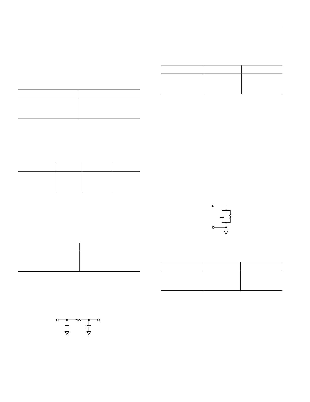
Figure 1 shows the assumed lumped - element model of
the LNA input. The simplied model reects the measured
port impedance values with an equivalent circuit of the
lowest possible complexity. A section with results is
given for both high sensitivity mode (LNAGAIN = 30)
and low current mode (LNAGAIN = 10).
Figure 1. LNA Lumped-Element Model, Rx Mode
For best sensitivit y, the source impedance should be
ma tched with the reco mmen ded CLC str u c ture to
maximize the differential voltage sw ing across the
termina l s RFIN and RF I N B . Thi s tas k sho u l d be
ac complished by means of an RF simulator with built- in
optimizer. The matching condition typically results in a
slightly reactive input reection coefcient.
LNA Input, Rx Mode, LNAGAIN = 30
Table 1 lists the component values of the equivalent
circuit shown in Figure 1 applicable for Rx mode and
LNAGAIN = 30 ([R9.DB20, R9.DB21] = [1,0]).
Table 1. Elements of LNA Equivalent Circuit (Figure 1)
in Rx Mode, LNAGAIN = 30
Frequency (MHz) Rplnarx () Cplnarx (pF) Cslnarx (pF)
433 to 435 300 2.0 0.1
868 to 870 180 2.3 0.1
902 to 928 175 2.3 0.1
REV. 0
Page 2

AN-764
–3–
AN-764
CplnatxCplnatx
RFINB
Rslnatx
RFIN
Rpparx
Cpparx
RFOUT
RFGND
REV. 0
Since the c apacitance Cslnar x is comparably low, the
LNA input impedance may be approximated as two
independent impedance elements between RFIN to GND
and RFINB to GND, respectively. This simplied model
is sufcient for the majority of matching problems. The
impedance values are listed in Table 2.
Table 2. Ground-Referred Input Impedance of LNA
in Rx Mode, LNAGAIN = 30
Frequency (MHz) Zlnarx_gnd ()
433 to 435 71 – j128
868 to 870 26 – j63
902 to 928 24 – j60
LNA Input, Rx Mode, LNAGAIN = 10
Table 3 lists the component values of the equivalent
circuit shown in Figure 1 applicable for Rx mode and
LNAGAIN = 10 ([R9.DB20, R9.DB21] = [0,1]).
Table 3. Elements of LNA Equivalent Circuit (Figure 1)
in Rx Mode, LNAGAIN = 10
Frequency (MHz) Rplnarx () Cplnarx (pF) Cslnarx (pF)
433 to 435 200 2.0 0.1
868 to 870 125 2.4 0.1
902 to 928 120 2.4 0.1
Again, a simplication of the model is possible if the
component s in the coupling branch between input
RFIN and RFINB are reected in two single - ended,
ground -referred branc hes . The values are given in
Table 4.
Table 5 lists the estimated component values for the
three frequency bands of interest.
Table 5. Elements of LNA Equivalent Circuit (Figure 2)
in Tx Mode
Frequency (MHz) Cplnatx (pF) Rslnatx ()
433 to 435 2.2 10
868 to 870 2.6 10
902 to 928 2.6 10
PA Output, Rx Mode
In Rx mode the parasitic capacitance of the biased PA
output is of interest for the design of the combined Rx/Tx
matching network. Figure 3 shows the lumped-element
model of the biased PA in Rx mode using the minimum
number of components. Since the ground connection
of the PA block is bonded directly to the paddle of
the IC package, the ground impedance is very low if
multiple vias are used between the paddle ground and
the ground plane of the printed circuit board. Therefore,
the impedance bet ween the RFGND pin and the ideal ized common ground node of the printed circuit board
may be neglected. Frequency-dependent component
values applicable for the equivalent circuit of Figure 3
are listed in Table 6. A bias voltage of 3 V has been used.
The PA port impedance shows a slight dependency on
the bias voltage.
Table 4. Ground-Referred Input Impedance of LNA
in Rx Mode, LNAGAIN = 10
Frequency (MHz) Zlnarx_gnd ()
433 to 435 82 – j98
868 to 870 30 – j53
902 to 928 28 – j51
LNA Input, Tx Mode
When the ADF7020 enters Tx mode, the Rx/Tx switch is
closed, providing a low impedance path between pins
RFIN and RFINB. For the design of the matching network,
the LNA input impedance in Tx mode may be modeled
as shown in Figure 2.
Figure 2. LNA Lumped-Element Model, Tx Mode
Figure 3. PA Lumped-Element Model for Rx Mode
Table 6. Elements of PA Equivalent Circuit (Figure 3)
in Rx Mode
Frequency (MHz) Rpparx () Cpparx (pF)
433 to 435 2000 2.2
868 to 870 680 2.1
902 to 928 650 2.1
–2–
REV. 0
Page 3

AN-764
LppatxRppatx
RFOUT
Zppatx_opt
PA
PA Output, Tx Mode, Optimum Load Impedance
The PA load impedance values have been optimized to
yield an output power of 10 dBm at the lowest possible
current consumption at a supply voltage of 3.0 V by
means of stub tuner-based approach.
Figure 4. Denition of the Optimum PA Load
Impedance and Lumped-Element Model
Table 7. Optimum PA Load Impedance (Figure 4)
for PO = 10 dBm at VDD = 3.0 V
Frequency (MHz) Zppatx_opt ()
433 to 435 54 + j94
868 to 870 48 + j54
902 to 928 39 + j61
Table 7 lists optimum PA load impedance values for
each frequency band, which satisfies the condition
st ate d earlier. Figure 4 illustrates the definition of
the optimum load impedance and a lumped - element
equivalent circuit. The component values that represent
the optimum load impedance are listed in Table 8.
Table 8. Lumped Element Model of Optimum PA
Load Impedance (Figure 4)
Frequency (MHz) Rppatx () Lppatx (pF)
433 to 435 218 46
868 to 870 110 18
902 to 925 134 15
SUMMARY
This application note presents measured port imped anc e values for the ADF7020. The measurements
cover the LNA input in different modes for the most
important frequencies and different gain settings. The
PA port impedance is characterized in its idle state in
Rx mode. For operation in Tx mode, the optimum PA
load impedance has been quantified. The provided
data satisfie s the requirements for the design of the
combined Rx/Tx matching network.
REV. 0
–3–
Page 4

AN05297–0–2/05(0)
© 2005 Analog Devices, Inc. All rights reserved. Trademarks and registered trademarks are the property of their respective owners.
–4–
 Loading...