

True Bipolar Input, Dual
Preliminary Technical Data
FEATURES
Dual 14-bit, 2-channel ADC
True Bipolar Analog Inputs
Programmable Input Ranges
±10, ±5, 0 to 10 V
Throughput rate: 1 MSPS
Simultaneous conversion with read in 1μs
Specified for V
Low current consumption: 5.65 mA max
Wide input bandwidth
14 bits No Missing Codes
On-chip reference: 2.5 V
–40°C to +85°C operation
High speed serial interface
SPI®/QSPI™/MICROWIRE™/DSP compatible
TM
iCMOS
24-lead TSSOP package
For 12 bit version see AD7366
GENERAL DESCRIPTION
of 5 V±5%
CC
Process Technology
1μs, 14-Bit, 2-Channel SAR ADC
AD7367
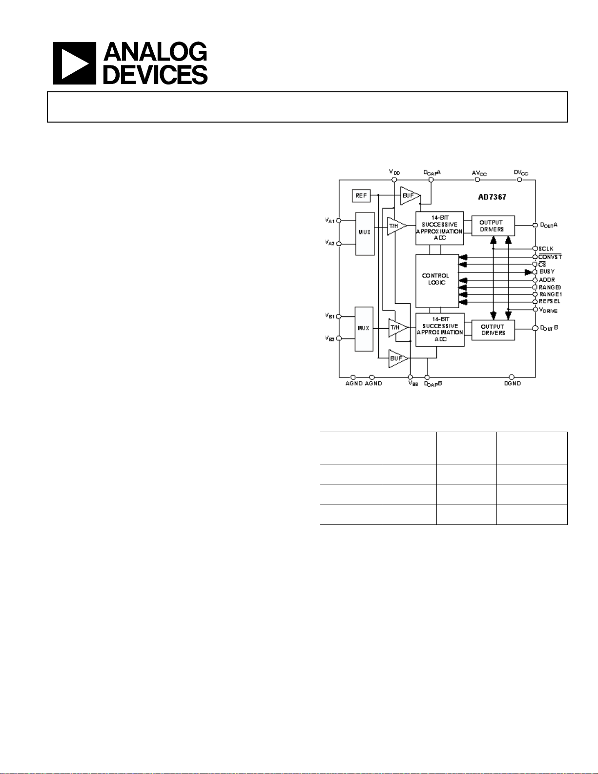
FUNCTIONAL BLOCK DIAGRAM
The AD73671 is a dual, 14-bit, high speed, low power, successive
approximation ADC that features throughput rates up to 1
MSPS. The device contains two ADCs, each preceded by a 2channel multiplexer, and a low noise, wide bandwidth trackand-hold amplifier that can handle input frequencies in excess
of 10 MHz.
Table 1.Related Products
Device
Resolution Throughput
Number
Figure 1
Rate
Number of
Channels
The AD7367 is fabricated on Analog Devices’ Industrial CMOS
process, iCMOS, a technology platform combining the
advantages of low and high voltage CMOS, bipolar and high
voltage DMOS processes. The process allows the AD7367 to
accept high voltage bipolar signals in addition to reducing
AD7366 12-Bit 1 MSPS Dual, 2-ch
AD7366-5 12-Bit 500 KSPS Dual, 2-ch
AD7367-5 14-Bit 500 KSPS Dual, 2-ch
power consumption and package size.
The AD7367 can accept true bipolar analog input signals in the
±10 V range, ±5 V range and 0 to 10 V range.
The AD7367 has an on-chip 2.5 V reference that can be
overdriven if an external reference is preferred. The AD7367 is
available in a 24-lead TSSOP package.
1
Protected by U.S. Patent No. 6,681,332.
TM
iCMOS
Process Technology
For analog systems designers within industrial/instrumentation equipment OEMs who need high performance ICs at higher-voltage levels, iCMOS is a technology
platform that enables the development of analog ICs capable of 30V and operating at +/- 15V supplies while allowing dramatic reductions in power consumption and
package size, and increased AC and DC performance.
Rev. PrD
Information furnished by Analog Devices is believed to be accurate and reliable. However, no
responsibility is assumed by Anal og Devices for its use, nor for any infringements of patents or ot her
rights of third parties that may result from its use. Specifications subject to change without notice. No
license is granted by implication or otherwise under any patent or patent rights of Analog Devices.
Trademarks and registered trademarks are the property of their respective owners.
One Technology Way, P.O. Box 9106, Norwood, MA 02062-9106, U.S.A.
Tel: 781.329.4700 www.analog.com
Fax: 781.461.3113 ©2006 Analog Devices, Inc. All rights reserved.

AD7367 Preliminary Technical Data
TABLE OF CONTENTS
FEATURES........................................................................................ 1
Analog Inputs ............................................................................. 11
GENERAL DESCRIPTION ............................................................ 1
FUNCTIONAL BLOCK DIAGRAM............................................. 1
Revision History ............................................................................... 2
Specifications..................................................................................... 3
Timing Specifications .................................................................. 5
Absolute Maximum Ratings............................................................ 6
ESD Caution.................................................................................. 6
Pin Configuration and Function Descriptions............................. 7
Terminology ...................................................................................... 9
Theory of operation ...................................................................10
REVISION HISTORY
4/06—PRA: Initial Version
5/06—PRA changes to PRB: Initial Version
10/06—PRB changes to PRC: Modified Supply specifications
V
............................................................................................ 12
DRIVE
Reference ..................................................................................... 12
Modes of Operation ....................................................................... 12
NORMAL MODE ...................................................................... 12
Shut-down Mode........................................................................ 12
POWER-UP TIMES................................................................... 12
Serial Interface ................................................................................ 12
Outline Dimensions....................................................................... 12
Ordering Guide............................................................................... 12
Rev. PrD | Page 2 of 16

AD7367 Preliminary Technical Data
SPECIFICATIONS
AVCC = DVCC =4.75 V to 5.25 V, VDD = 11.5 V to 16.5 V, VSS = −11.5 V to −16.5 V, V
V
= 2.5 V Internal/External; TA = T
REF
MIN
to T
, unless otherwise noted1.
MAX
Table 2.
Parameter Min Typ Max Unit Test Conditions/
DYNAMIC PERFORMANCE fIN = 50 kHz sine wave;
Signal-to-Noise Ratio (SNR)
Signal-to-Noise + Distortion Ratio
2
(SINAD)
Total Harmonic Distortion (THD)
Spurious Free Dynamic Range (SFDR)
Intermodulation Distortion (IMD)
2
TDB 79 dB
TBD 78 dB
2
2
2
-85 TBD dB
-85 TBD dB
fa = 49 kHz, fb = 51 kHz
Second Order Terms -91 dB
Third Order Terms
Channel-to-Channel Isolation
2
-89 dB
-88 dB
SAMPLE AND HOLD
Aperture Delay3 10 ns
Aperture Jitter3 40 ps
Aperture Delay Matching3 100 ps
Full Power Bandwidth 65 MHz @ 3 dB, ±10 V range
15 MHz @ 0.1 dB, ±10 V range
DC ACCURACY
Resolution 14 Bits
Integral Nonlinearity
Differential Nonlinearity
2
2
±2 LSB
±0.99 LSB Guaranteed no missed codes to 14 bits
Positive Full Scale Error2 ±5 LSB
Positive Full Scale Error Match2 ±0.5 LSB
Zero Code Error2 ±1 LSB
Zero Code Error Match2 ±1 LSB
Negative Full Scale Error2 ±5 LSB
Negative Full Scale Error Match2 ±0.5 LSB
ANALOG INPUT
Input Voltage Ranges ±10 V
(Programmed via RANGE Pins) ±5 V
0 to
10V
See Table 6.
DC Leakage Current ±1 µA
Input Capacitance 12 p When in track, ±10 V range
15 pF When in track, ±5 V or 0 to 10 V range
3 pF When in hold
Input impedance 260 KΩ For ±10V @1 Msps
2.3 MΩ For ±10V @100 Ksps
125 KΩ For ±5 / 0-10V @1 Msps
1.1 MΩ For ±5 / 0-10V @100Ksps
= 2.7 V to 5.25V, f
DRIVE
V
SAMPLE
= 1MSPS, f
= 48MHz,
SCLK
Comments
= +11.5V min, VSS = −11.5V min, VCC
V
DD
= 4.75V to 5.25V
= +11.5V min, VSS = −11.5V min, VCC
V
DD
= 4.75V to 5.25V
= +11.5V min, VSS = -11.5V min, VCC
V
DD
= 4.75V to 5.25V
Rev. PrD | Page 3 of 16

AD7367 Preliminary Technical Data
Parameter Min Typ Max Unit Test Conditions/
Comments
REFERENCE INPUT/OUTPUT
Reference Output Voltage
Reference Input Voltage Range +2.5 3.0 V
DC Leakage Current ±1 µA
Input Capacitance 25 pF
V
A, V
REF
B Output Impedance
REF
Reference Temperature Coefficient 10 20 ppm/°C
V
Noise 20 µV
REF
LOGIC INPUTS
Input High Voltage, V
Input Low Voltage, V
Input Current, IIN ±1 µA max VIN = 0 V or V
Input Capacitance, C
LOGIC OUTPUTS
Output High Voltage, VOH V
Output Low Voltage, VOL 0.4 V
Floating State Leakage Current ±1 µA
Floating State Output Capacitance
CONVERSION RATE
Conversion Time 680 ns
Track/Hold Acquisition Time
Throughput Rate 1 MSPS For 4.75V≤V
900 KSPS For 2.7V≤V
POWER REQUIREMENTS Digital I/Ps = 0 V or V
V
CC
V
DD
V
SS
V
2.7 5.25 V
DRIVE
Normal Mode (Static)
IDD 250 µA VDD = +16.5 V
ISS 50 µA VSS = −16.5 V
ICC 1.8 mA VCC = 5.5 V
Normal Mode (Operational) fs = 1 MSPS
IDD 925 µA VDD = +16.5 V
ISS 725 µA VSS = −16.5 V
ICC 4 mA VCC = 5.25 V, internal reference enabled
Shut-Down Mode
IDD 1 µA VDD = +16.5 V
ISS 1 µA VSS = −16.5 V
ICC 1 µA VCC = 5.25 V
Power Dissipation
Normal Mode (Operational) 48.23 mW VDD = +16.5V, VSS = −16.5V, VCC = 5.25V
Shut-Down 15 µW VDD = +5V, VSS = −5V, VCC = 5V
Shut-Down 38.25 µW VDD = +16.5V, VSS = −16.5V, VCC = 5.25
1
Temperature range is −40°C to +85°C
2
See Terminology section.
3
Sample tested during initial release to ensure compliance.
4
Refers to pins V
REF
A or V
REF
4
2.5 2.5 V ±0.2% max @ 25°C
External reference applied to Pin
A/Pin V
V
REF
0.7× V
INH
0.8 V max
INL
3
IN
3
10 Ω
RMS
V min
DRIVE
5 pF typ
− 0.2 V
DRIVE
3
10 pF
140 ns Full-scale step input;
4.75 5.25 V See Table 6
+11.5 +16.5 V See Table 6
-16.5 -11.5 V See Table 6
B.
REF
DRIVE
DRIVE
B
DRIVE
≤5.25V, f
<4.75V , f
DRIVE
= 48MHz
SCLK
= 35MHz
SCLK
Rev. PrD | Page 4 of 16

AD7367 Preliminary Technical Data
TIMING SPECIFICATIONS
AVCC = DVCC =4.75 V to 5.25 V, VDD = 11.5V to 16.5 V, VSS = −11.5V to −16.5 V, V
otherwise noted
1
.
Table 3.
, T
Parameter Limit at T
2.7V≤V
t
CONVER T
680 680 ns max
<4.75V 4.75V≤V
DRIVE
MIN
Unit Test Conditions / Comments
MAX
≤5.25V
DRIVE
Conversion time, Internal clock. CONVST
edge
f
SCLK
35 48
10 10 kHz min Frequency of serial read clock.
MHz
max
t
30 30 ns min
QUIET
Minimum quiet time required between end of serial read and start of
next conversion
t1 10 10 ns min
t
2
t
3
5 5 ns min
0 0 ns min
Minimum CONVST
CONVST
falling edge to BUSY rising edge.
BUSY falling edge to MSB valid once CS is low for t4 prior to BUSY going
Low
t
4
10 10 ns max
Delay from CS
disabled
2
t
5
20 14 ns max Data access time after SCLK falling edge
t6 5 5 ns min SCLK to data valid hold time
t7 0.1 t
t8 0.1 t
t
9
t
10
10 10 ns max
5 5 ns min SCLK falling edge to DOUTA, DOUTB, high impedance
SCLK
0.1 t
SCLK
0.1 t
SCLK
ns min SCLK high pulse width
SCLK
ns min SCLK low pulse width
rising edge to DOUTA, DOUTB, high impedance
CS
10 10 ns max SCLK falling edge to DOUTA, DOUTB, high impedance
t
POWER-UP
70 70 μs
Power up time from shutdown mode. Time required between CONVST
rising edge and CONVST falling edge.
1
Sample tested during initial release to ensure compliance. All input signals are specified with tr = tf = 5 ns (10% to 90% of VDD) and timed from a voltage level of 1.6 V.
All timing specifications given are with a 25 pF load capacitance. With a load capacitance greater than this value, a digital buffer or latch must be used. See
Terminology section and Figure 9.
2
The time required for the output to cross 0.4 V or 2.4 V.
= 2.7 V to 5.25V, TA = T
DRIVE
MIN
to T
MAX
, unless
falling edge to BUSY falling
Low pulse.
falling edge until DOUTA and DOUTB are three-state
Rev. PrD | Page 5 of 16

AD7367 Preliminary Technical Data
ABSOLUTE MAXIMUM RATINGS
Table 4
Parameter Rating
VDD to AGND, DGND −0.3 V to +16.5 V
VSS to AGND, DGND −0.3 V to +16.5 V
V
to DGND −0.3 V to DVDD
DRIVE
VDD to AVcc Vcc – 0.3V to +16.5V
AVCC to AGND, DGND -0.3V to +7V
DVCC to AVCC -0.3 V to + 0.3V
DVCC to DGND -0.3 V to + 7V
V
to AGND −0.3 V to DVCC
DRIVE
AGND to DGND −0.3 V to +0.3 V
Analog Input Voltage to AGND VSS −0.3 V to VDD + 0.3 V
Digital Input Voltage to DGND −0.3 V to V
Digital Output Voltage to GND −0.3 V to V
V
A, V
B input to AGND −0.3 V to AVCC + 0.3 V
REF
REF
Input Current to Any Pin
Except Supplies
1
±10 mA
Operating Temperature Range −40°C to +85°C
Storage Temperature Range −65°C to +150°C
Junction Temperature 150°C
TSSOP Package
θJA Thermal Impedance 128°C/W
θJC Thermal Impedance 42°C/W
Pb-free Temperature, Soldering
Reflow 260(+0)°C
ESD TBD kV
1
Transient currents of up to 100 mA will not cause latch up.
ESD CAUTION
ESD (electrostatic discharge) sensitive device. Electrostatic charges as high as 4000 V readily accumulate on
the human body and test equipment and can discharge without detection. Although this product features
proprietary ESD protection circuitry, permanent damage may occur on devices subjected to high energy
electrostatic discharges. Therefore, proper ESD precautions are recommended to avoid performance
degradation or loss of functionality.
DRIVE
DRIVE
+ 0.3 V
+ 0.3 V
Rev. PrD | Page 6 of 16

Preliminary Technical Data AD7367
PIN CONFIGURATION AND FUNCTION DESCRIPTIONS
D
A
Table 5. Pin Function Descriptions
Pin No. Mnemonic Description
1
OUT
V
2
DRIVE
DV
3
CC
RANGE1
RANGE0
ADDR
4
AD7367
5
TOP VIEW
6
AGND
AV
D
CAP
V
V
V
(Not to S cale)
7
8
CC
AD
9
10
SS
11
A1
12
A2
Figure 2 24-Lead RU-24.
24
23
22
21
20
19
18
17
16
15
14
13
DGND
D
B
OUT
BUSY
CNVST
SCLK
CS
REFSEL
AGND
B
CAP
V
DD
V
B1
V
B2
1, 23 D
A,
OUT
D
B
OUT
Serial Data Outputs. The data output is supplied to each pin as a serial data stream. The bits are clocked out
on the falling edge of the SCLK input and 14 SCLK cycles are required to access the data. The data
simultaneously appears on both pins from the simultaneous conversions of both ADCs. The data stream
consists of the 14 bits of conversion data and is provided MSB first. If
cycles on either D
OUT
A or D
B, the data from the other ADC follows on the D
OUT
from a simultaneous conversion on both ADCs to be gathered in serial format on either D
CS
is held low for a further 14 SCLK
pin. This allows data
OUT
A or D
OUT
OUT
B
using only one serial port. See the Serial Interface section.
2 V
Logic Power Supply Input. The voltage supplied at this pin determines at what voltage the interface will
DRIVE
operate. This pin should be decoupled to DGND. The voltage range on this pin is 2.7V to 5.25V and may be
different to that at AV
throughput rate of 1Msps V
and DVCC but should never exceed either by more than 0.3V To achieve a
CC
must be greater than or equal to 4.75V
DRIVE
3 DVCC Digital Supply Voltage, 4.75V to 5.25V. The DVCC and AVCC voltages should ideally be at the same potential.
For best performance it is recommended that DV
and AVCC pins be shorted together, to ensure the voltage
CC
difference between them never exceed 0.3 V even on a transient basis. This supply should be decoupled to
DGND. 10 µF and 100 nF decoupling capacitors should be placed on the DV
4,5 RANGE0,
RANGE1
Analog Input Range Selection. Logic inputs. The polarity on these pins determines the input range of the
analog input channels. See Analog Inputs section and Table 7 for details
CC
pin.
6 ADDR Multiplexer Select. Logic input. This input is used to select the pair of channels to be simultaneously
converted, either Channel 1 of both ADC A and ADC B, or Channel 2 of both ADC A and ADCB. The logic
state on this pin is latched on the rising edge of BUSY to set up the multiplexer for the next conversion.
7,17 AGND Analog Ground. Ground reference point for all analog circuitry on the AD7367. All analog input signals and
any external reference signal should be referred to this AGND voltage. Both AGND pins should connect to
the AGND plane of a system. The AGND and DGND voltages ideally should be at the same potential and
must not be more than 0.3 V apart, even on a transient basis.
8 AVCC
9,16 D
CAP
D
CAP
A,
B
Analog Supply Voltage, 4.75 V to 5.25 V. This is the supply voltage for the ADC cores. The AV
voltages ideally should be at the same potential. For best performance it is recommended that DV
AV
pins be shorted together, to ensure the voltage difference between them never exceed 0.3 V even on a
CC
and DVCC
CC
and
CC
transient basis. This supply should be decoupled to AGND. 10 µF and 100 nF decoupling capacitors should
be placed on the AV
CC
pins.
Decoupling Capacitor Pins. Decoupling capacitors are connected to these pins to decouple the reference
buffer for each respective ADC. For best performance it is recommended to use 680nF decoupling capacitor
on these pins. Provided the output is buffered, the on-chip reference can be taken from these pins and
Rev. PrD | Page 7 of 16

AD7367 Preliminary Technical Data
applied externally to the rest of a system.
10 VSS Negative power supply voltage. This is the negative supply voltage for the Analog Input section. The supply
must be less than a maximum voltage of -11.5V for all input ranges. See Table 6 for further details. 10 µF and
CAP
pin.
SS
B pins.
A, and D
OUT
DD
OUT
pin.
B.
A and Pin D
CAP
CS
is logic low the
CAP
B
100 nF decoupling capacitors should be placed on the V
11,12 VA1, VA2 Analog Inputs of ADC A. These are both single-ended analog inputs. The Analog input range on these
channels is determined by the RANGE0 and RANGE1 pins.
13,14 VB2, VB1 Analog Inputs of ADC B. These are both single-ended analog inputs. The Analog input range on these
channels is determined by the RANGE0 and RANGE1 pins.
15 VDD Positive power supply voltage. This is the positive supply voltage for the Analog Input section. The supply
must be greater than a minimum voltage of 11.5V for all the analog input ranges. See Table 6 for further
details. 10 µF and 100 nF decoupling capacitors should be placed on the V
18 REFSEL Internal/External Reference Selection. Logic input. If this pin is tied to a logic high, the on-chip 2.5 V
reference is used as the reference source for both ADC A and ADC B. In addition, Pin D
must be tied to decoupling capacitors. If the REF SELECT pin is tied to GND, an external reference can be
19
CS
supplied to the AD7367 through the D
Chip Select. Active low logic input. This input frames the serial data transfer. When
A and/or D
CAP
output bus is enabled and the conversion result is output on D
20 SCLK Serial Clock. Logic input. A serial clock input provides the SCLK for accessing the data from the AD7367.
21
CONVST
Conversion Start. Edge triggered logic input. On the falling edge of this input the track/hold goes into hold
mode and conversion is initiated. If
CONVST
down mode. In this case, the rising edge of
is low at the end of a conversion, the part goes into power-
CONVST
will instruct the part to power up again.
22 BUSY BUSY Output. Transitions high when a conversion is started and remains high until the conversion is
complete.
24 DGND Digital Ground. This is the ground reference point for all digital circuitry on the AD7367. The DGND pin
should connect to the DGND plane of a system. The DGND and AGND voltages should ideally be at the
same potential and must not be more than 0.3 V apart, even on a transient basis.
Rev. PrD | Page 8 of 16

Preliminary Technical Data AD7367
TERMINOLOGY
Differential Nonlinearity
Differential nonlinearity is the difference between the measured
and the ideal 1 LSB change between any two adjacent codes in
the ADC.
Integral Nonlinearity
Integral nonlinearity is the maximum deviation from a straight
line passing through the endpoints of the ADC transfer function.
The endpoints of the transfer function are zero scale, a single
(1) LSB point below the first code transition and full scale, a
point 1 LSB above the last code transition.
Zero Code Error
It is the deviation of the midscale transition (all 1s to all 0s)
from the ideal V
ranges and 2×V
voltage, i.e., AGND – 1/2 LSB for bipolar
IN
−1LSB for the unipolar range.
REF
Positive Full Scale Error
It is the deviation of the last code transition (011…110) to
(011…111) from the ideal ( +4 × V
LSB) after the Zero Code Error has been adjusted out.
- 1 LSB or + 2 x V
REF
– 1
REF
Negative Full Scale Error
This is the deviation of the first code transition (10…000) to
(10…001) from the ideal (i.e., - 4 x V
+ 1 LSB, - 2 x V
REF
REF
+ 1
LSB or AGND + 1LSB) after the Zero Code Error has been
adjusted out.
Zero Code Error Match
This is the difference in zero code error across all 12 channels.
Positive Full Scale Error Match
This is the difference in positive full scale error across all
channels.
Negative Full Scale Error Match
This is the difference in negative full-scale error across all
channels.
Track-and-Hold Acquisition Time
The track-and-hold amplifier returns to track mode at the end
of conversion. Track-and-hold acquisition time is the time
required for the output of the track-and-hold amplifier to reach
its final value, within ±1/2 LSB, after the end of conversion.
Signal to (Noise + Distortion) Ratio
This ratio is the measured ratio of signal to (noise + distortion)
at the output of the A/D converter. The signal is the rms
amplitude of the fundamental. Noise is the sum of all nonfundamental signals up to half the sampling frequency (f
/2),
S
excluding dc. The ratio is dependent on the number of
quantization levels in the digitization process; the more levels,
the smaller the quantization noise. The theoretical signal to
(noise + distortion) ratio for an ideal N-bit converter with a sine
wave input is given by:
Rev. PrD | Page 9 of 16
Signal to (Noise + Distortion) = (6.02N + 1.76) dB
Thus for a 12-bit converter, this is 74 dB.
Total Harmonic Distortion (THD)
Total harmonic distortion is the ratio of the rms sum of
harmonics to the fundamental. For the AD7367, it is defined as:
2
dBTHD
=
where V
V
is the rms amplitude of the fundamental and V2, V3,
1
, V5 and V6 are the rms amplitudes of the second through the
4
2
log20)(
4
3
V
1
VVVVV
++++
6
5
2
2
2
2
sixth harmonics.
Peak Harmonic or Spurious Noise
Peak harmonic, or spurious noise, is defined as the ratio of the
rms value of the next largest component in the ADC output
spectrum (up to f
/2, excluding dc) to the rms value of the
S
fundamental. Normally, the value of this specification is
determined by the largest harmonic in the spectrum, but for
ADCs where the harmonics are buried in the noise floor, it is a
noise peak.
Channel-to-Channel Isolation
Channel-to-channel isolation is a measure of the level of
crosstalk between any two channels when operating in the +/10 V Range. It is measured by applying a full-scale, 150 kHz
sine wave signal to all unselected input channels and
determining how much that signal is attenuated in the selected
channel with a 50 kHz signal. The figure given is the worst-case
across all four channels for the AD7367. See also Typical
Performance Characteristics.
Intermodulation Distortion
With inputs consisting of sine waves at two frequencies, fa and
fb, any active device with nonlinearities will create distortion
products at sum, and difference frequencies of mfa ± nfb where
m, n = 0, 1, 2, 3, and so on. Intermodulation distortion terms
are those for which neither m nor n are equal to zero. For
example, the second order terms include (fa + fb) and (fa − fb),
while the third order terms include (2fa + fb), (2fa − fb), (fa +
2fb) and (fa − 2fb).
The AD7367 is tested using the CCIF standard where two input
frequencies near the top end of the input bandwidth are used.
In this case, the second order terms are usually distanced in
frequency from the original sine waves, while the third order
terms are usually at a frequency close to the input frequencies.
As a result, the second and third order terms are specified
separately. The calculation of the intermodulation distortion is
as per the THD specification, where it is the ratio of the rms
sum of the individual distortion products to the rms amplitude
of the sum of the fundamentals expressed in dBs.

AD7367 Preliminary Technical Data
PSRR (Power Supply Rejection)
Variations in power supply affect the full-scale transition but
not the converter’s linearity. Power supply rejection is the
maximum change in the full-scale transition point due to a
change in power supply voltage from the nominal value (see
figure x).
THEORY OF OPERATION
Circuit Information
The AD7367 is a fast, dual, 2-Channel, 14-bit, Bipolar Input,
Serial A/D converter. The AD7367 can accept bipolar input
ranges of ±10V and ±5V. It can also accept a 0 to 10V unipolar
input range. The AD7367 requires V
and V
DD
the high voltage analog input structure. These supplies must be
equal to or greater than 11.5V. See Table 6 for the minimum
requirements on these supplies for each Analog Input Range.
The AD7367 requires a low voltage 4.75V to 5.25 V V
to power the ADC core.
Table 6. Reference and Supply Requirements for each Analog
Input Range
Selected
Analog
Input
Range (V)
Reference
Voltage
(V)
Full
Scale
Input
Range(V)
2.5 ±10 5 ±11.5
±10
3.0 ±12 5 ±12
dual supplies for
SS
AV
CC
(V)
supply
CC
Minimum
VDD/V
SS
(V)
up the REFSEL pin must be tied to either a high or low logic
state to select either the internal or external reference option. If
the internal reference is the preferred option, the user must tie
the REFSEL pin logic high. Alternatively, if REFSEL is tied to
GND then an external reference can be supplied to both ADC’s
through D
CAP
A & D
B pins.
CAP
The analog inputs are configured as two single ended inputs for
each ADC. The various different input voltage ranges can be
selected by programming the RANGE bits as shown in Table 7.
The AD7367 also features power-down option to allow power
saving between conversions. The power-down feature is
implemented via the
CONVST
pin as described in the Modes of
Operation section.
Converter Operation
The AD7367 has two successive approximation analog-todigital converters, each based around two capacitive DACs.
Figure 3 and Figure 4 show simplified schematics of one of
these ADCs in acquisition and conversion phase, respectively.
The ADC is comprised of control logic, a SAR, and two
capacitive DACs. In Figure 3 (the acquisition phase), SW2 is
closed and SW1 is in Position A, the comparator is held in a
balanced condition, and the sampling capacitor arrays acquire
the signal on the input.
CAPACITIVE
DAC
± 5
2.5 ±5 5 ±11.5
3.0 ±6 5 ±11.5
2.5 0 to 10 5 ±11.5 0 to 10
3.0 0 to 12 5 ±12
The AD7367 contains two on-chip differential track-and-hold
amplifiers, two successive approximation A/D converters, and a
serial interface with two separate data output pins. It is housed
in a 24-lead TSSOP package, offering the user considerable
space-saving advantages over alternative solutions. The AD7367
requires a
CONVST
edge of
CONVST
signal to start conversion. On the falling
both track-and-holds will be placed into hold
mode and the conversions are initiated. The BUSY signal will go
high to indicate the conversions are taking place. The clock
source for each successive approximation ADC is provided by
an internal oscillator. The BUSY signal will go low to indicate
the end of conversion. On the falling edge of BUSY the trackand-hold will return to track mode. Once the conversion is
finished, the serial clock input accesses data from the part.
The AD7367 has an on-chip 2.5 V reference that can be
overdriven when an external reference is preferred. If the
internal reference is to be used elsewhere in a system, then the
output from D
CAP
A & D
B must first be buffered. On Power
CAP
Rev. PrD | Page 10 of 16
V
AGND
IN
A
SW1
B
Figure 3 ADC Acquisition Phase
SW2
COMPARATOR
When the ADC starts a conversion (Figure 4), SW2 opens and
SW1 moves to Position B, causing the comparator to become
unbalanced. The control logic and the charge redistribution
DACs are used to add and subtract fixed amounts of charge
from the sampling capacitor to bring the comparator back into a
balanced condition. When the comparator is rebalanced, the
conversion is complete. The control logic generates the ADC
output code.
CONTROL
LOGIC

Preliminary Technical Data AD7367
V
V
CAPACITIVE
DAC
SW1
A
CONTROL
B
SW2
COMPARATOR
LOGIC
V
AGND
IN
Figure 4 ADC Conversion Phase
ANALOG INPUTS
Each ADC in the AD7367 has two Single Ended Analog Inputs.
Figure 5 shows the equivalent circuit of the analog input
structure of the AD7367. The two diodes provide ESD
protection. Care must be taken to ensure that the analog input
signals never exceed the supply rails by more than 300 mV. This
causes these diodes to become forward-biased and starts
conducting current into the substrate. These diodes can
conduct up to 10 mA without causing irreversible damage to
the part. Capacitor C1 in Figure 5 is typically 5 pF and can
primarily be attributed to pin capacitance. The resistors are
lumped components made up of the on resistance of the
switches. The value of these resistors is typically about TBD Ω.
Capacitor C2 is the ADC’s sampling capacitors with a
capacitance of approximately TBD pF for the ±10V input range
and approximately TBD pF for all other input ranges.
DD
D
0
IN
C1
D
V
SS
Figure 5 Equivalent Analog Input Structure
The AD7367 can handle true bipolar input voltages. The Analog
input can be set to one of three ranges; ±10V, ±5V, 0-10V. The
logic levels on pins RANGE0 and RANGE1 determine which
input range is selected as outlined in Table 7. These range bits
should not be changed during the acquisition time prior to a
conversion but may change at any other time.
Table 7. Analog Input Range Selection
RANGE1 RANGE0 Range Selected
0 0 ±10V
0 1 ±5V
1 0 0 to 10V
R1
C2
04852-023
The AD7367 requires V
voltage analog input structures. These supplies must be equal to
or greater than ±11.5V. See Table 6 for the requirements on
these supplies. The AD7367 requires a low voltage 4.75V to 5.25
supply to power the ADC core, a 4.75V to 5.25V DVCC
V AV
CC
supply for the Digital Power and a 2.7V to 5.25V V
for the interface power.
Channel selection is made via the ADDR pin as shown in
Table 8. The logic level on the ADDR pin is latched on the rising
edge of BUSY for the next conversion, not the one in progress.
When power is first supplied to the AD7367 the default channel
selection will be V
Table 8. Channel Selection
ADDR Channels Selected
0 VA1, VB1
1 VA2, VB2
Transfer Function
The AD7367 output coding is two’s complement. The designed
code transitions occur at successive integer LSB values (i.e. 1
LSB, 2 lSB, and so on). The LSB size is dependant on the analog
input range selected.
Table 9 LSB sizes for each Analog Input Range.
Input Range Full Scale Range/4096 LSB Size
±10 V 20 V/16384 1.22mV
±5 V 10 V/16384 0.61mV
0 to 10 V 10V/16384 0.61mV
The ideal transfer characteristic is shown in Figure 6
011...111
011...110
E
D
000...001
O
000...000
C
C
111...111
D
A
100...010
100...001
100...000
and VSS dual supplies for the high
DD
and VB1.
A1
-FSR/2
+ 1LSB
ANALOG INPUT
Figure 6.Transfer Characteristic
0V
+FSR/2 - 1LSB
DRIVE
supply
1 1 Do not program
Rev. PrD | Page 11 of 16

AD7367 Preliminary Technical Data
V
DRIVE
The AD7367 also has a V
which the serial interface operates. V
feature to control the voltage at
DRIVE
allows the ADC to
DRIVE
easily interface to both 3 V and 5 V processors. For example, if
the AD7367 was operated with a V
of 5 V, the V
CC
pin could
DRIVE
be powered from a 3 V supply, allowing a large dynamic range
with low voltage digital processors. Thus, the AD7367 could be
used with the ±10 V input range while still being able to
interface to 3 V digital parts.
To achieve the maximum throughput rate of 1Msps V
DRIVE
must
be greater than or equal to 4.75V, see table 3. The maximum
throughput rate for the AD7367 with the V
voltage set to
DRIVE
less than 4.75 and greater than 2.7 is 900 Ksps.
REFERENCE
The AD7367 can operate with either the internal 2.5 V on-chip
reference or an externally applied reference. The logic state of
the REFSEL pin determines whether the internal reference is
used. The internal reference is selected for both ADC when the
REFSEL pin is tied to logic high. If the REFSEL pin is tied to
GND then an external reference can be supplied through the
D
A and D
CAP
B pins. On power-up, the REFSEL pin must be
CAP
tied to either a low or high logic state for the part to operate.
Suitable reference sources for the AD7367 include AD780,
AD1582, ADR431, REF193, and ADR391.
The internal reference circuitry consists of a 2.5 V band gap
reference and a reference buffer. When operating the AD7367
in internal reference mode, the 2.5 V internal reference is
available at D
A and D
CAP
B pins, which should be decoupled
CAP
to AGND using a 680nF capacitor. It is recommended that the
internal reference be buffered before applying it elsewhere in
the system. The internal reference is capable of sourcing up to
150 μA with an analog input range of ±10 and 60 μA for both
the ±5V and 0-10V ranges.
If the internal reference operation is required for the ADC
conversion, the REFSEL pin must be tied to logic high on
power-up. The reference buffer requires 500 µs to power up and
charge the 680nF decoupling capacitor during the power-up
time.
The AD7367 is specified for a 2.5 V to 3 V reference range.
When a 3V reference is selected, the ranges are ±12 V, ±6 V, and
0 V to +12 V. For these ranges, the V
and VSS supply must be
DD
equal to or greater than the +12V &-12V respectively.
Rev. PrD | Page 12 of 16

AD7367 Preliminary Technical Data
MODES OF OPERATION
The mode of operation of the AD7367 is selected by the (logic) state of the
CONVST
possible modes of operation: normal mode and shut-down mode. These modes of operation are designed to provide flexible power
management options. These options can be chosen to optimize the power dissipation/throughput rate ratio for differing application
requirements.
signal at the end of a conversion. There are two
NORMAL MODE
This mode is intended for applications needing fast throughput
rates since the user does not have to worry about any power-up
times with the AD7367 remaining fully powered at all times.
Figure 7 shows the general mode of operation of the AD7367 in
this mode.
The conversion is initiated on the falling edge of
CONVST
described in the Circuit Information section. To ensure that the
part remains fully powered up at all times,
CONVST
logic state high prior to the BUSY signal going low. If
is at logic state low when the BUSY signal goes low, the
analogue circuitry will power down and the part will cease
converting. The BUSY signal remain high for the duration of
the conversion subsequently fourteen serial clock cycles are
required to read the conversion result. The D
three-state when
cycles has elapsed. If
CS
is brought high and not after 14 SCLK
CS
is left low for a further 14 SCLK cycles,
lines return to
OUT
t
1
CONVST
t
BUSY
2
t
CS
as
must be at
CONVST
convert
the result from the other on chip ADC is also accessed on the
same D
line, as shown in Figure 10(see the Serial Interface
OUT
section)
Once 28 SCLK cycles have elapsed, the D
CS
three-state when
falling edge. If
is brought high and not on the 28th SCLK
CS
is brought high prior to this, the D
returns to three-state at that point. Thus,
line returns to
OUT
OUT
CS
must be brought
line
high once the read is completed, as the bus does not
automatically return to three-state upon completion of the dual
result read.
Once a data transfer is complete and D
A and D
OUT
OUT
B have
returned to three-state, another conversion can be initiated after
the quiet time, t
, has elapsed by bringing
QUIET
CONVST
low
again.
t
quiet
t
3
SCLK
SERIAL READ OPERATION
Figure 7. Normal Mode Operation
SHUT-DOWN MODE
This mode is intended for use in applications where slow
throughput rates are required. This mode is suited to
applications where a series of conversions performed at a
relatively high throughput rate are followed by a long period of
inactivity and thus, shut-down. When the AD7367 is in full
power-down, all analog circuitry is powered down. As already
stated, the falling edge of
CONVST
The BUSY output subsequently goes high to indicate that the
conversion is in progress. Once the conversion is completed, the
BUSY output returns low. If the
initiates the conversion.
CONVST
signal is at logic low
Rev. PrD | Page 13 of 16
1
14
when BUSY goes low then the part will enter shut-down at the
end of the conversion phase. While the part is in shut-down
mode the digital output code from the last conversion on each
ADC can still be read from the D
CS
must be brought low as described in the Serial Interface
Section. The D
pins return to three-state once CS is brought
OUT
pins. To read the D
OUT
back to logic high.
To exit full power-down and power up the AD7367, A rising
edge of
has elapsed,
CONVST
is required. After the required power up time
CONVST
may be brought low again to initiate
OUT
data

AD7367 Preliminary Technical Data
another conversion, as shown in Figure 8. See the Power up
CONVST
t
BUSY
CS
2
t
convert
ENTERS SHUT-DOWN
time section for power-up times associated with the AD7367.
t
power-up
t
3
SCLK
Figure 8. Auto-Shutdown Mode
POWER-UP TIMES
The AD7367 has one power down mode, which has already
been described in detail. This section deals with the power-up
time required when coming out of this modes. It should be
noted that the power-up time, as explained in this section,
applies with the recommended capacitors in place on the D
and D
B pins. To power up from shut-down,
CAP
CONVST
be brought high and remain high for a minimum of 100μs, as
shown in Figure 8.
When power supplies are first applied to the AD7367, the ADC
may power up with
CONVST
state. Before attempting a valid conversion
in either the low or high logic
CONVST
brought high and remain high for the recommended power up
time of 100μs, it can then be brought low to initiate a
CAP
must
must be
1 14
conversion. With the AD7367 no dummy conversion is
required before valid data can be read from the
is intended to place the part in shut-down mode when the
supplies are first applied, then the AD7367 must be powered up
as explained about and a conversion initiated, but
A
should remain in the logic low state and when the BUSY signal
goes low thus the part enters shut-down.
Once supplies are applied to the AD7367, enough time must be
allowed for any external reference to power up and charge the
various reference buffer decoupling capacitors to their final values.
SERIAL READ OPERATION
D
OUT
CONVST
pins. If it
Rev. PrD | Page 14 of 16

Preliminary Technical Data AD7367
SERIAL INTERFACE
Figure 9 shows the detailed timing diagram for serial interfacing to the AD7367. On the falling edge of
CONVST
the
AD7367 will simultaneously convert the selected channels.
These conversions are performed using the on-chip oscillator.
After the falling edge of
CONVST
the BUSY signal goes high,
indicating the conversion has started. It returns low once the
conversion has been completed. The data can now be read from
the
D
pins.
OUT
CS and SCLK signals are required to transfer data from the
AD7367. The AD7367 has two output pins corresponding to
each ADC. Data can be read from the AD7367 using both
D
OUT
A & D
B, alternatively a single output pin of your
OUT
choice can be used. The SCLK input signal provides the
clock source for the serial interface. The
access data from the AD7367. The falling edge of
CS
goes low to
CS
takes
the bus out of three-state and clocks out the MSB of the
conversion result. The data stream consists of 14 bits of data
MSB first. The first bit of the conversion result is valid on the
first SCLK falling edge after the
CS
falling edge. The
subsequent 13 bits of data are clocked out on the falling edge
of the SCLK signal. A minimum of 14 Clock pulses must be
provided to AD7367 to access each conversion result.
9
shows how a 14 SCLK read is used to access the conversion
results.
On the rising edge of
and D
OUT
A and D
CS
, the conversion will be terminated
B go back into three-state. If CS is not
OUT
brought high, but is instead held low for a further 14 SCLK
cycles on either D
ADC follows on the D
where the case for D
A or D
OUT
OUT
A is shown. In this case, the D
OUT
B, the data from the other
OUT
pin. This is illustrated in Figure 10
line in use goes back into three-state on the rising edge of
If the falling edge of SCLK coincides with the falling edge of
CS
, then the falling edge of SCLK is not acknowledged by
the AD7367, and the next falling edge of the SCLK will be
the first registered after the falling edges of the
The CS pin can be brought low before the BUSY signal goes
low indicating the end of a conversion. This feature can be
utilized to ensure that the MSB is valid on the falling edge of
BUSY by bring
BUSY signal goes low. The dotted
CS
low a minimum of t4 nanoseconds before the
CS
line in Table 7 illustrates
this.
CS
.
Figure
OUT
CS
SCLK
D
OUT
D
D
CS
SCLK
OUT
OUT
CS
A
A
3-STATE
B
THREESTATE
DB13
DB13
1
DB12
A
t
8
t
9
DB0
14
3-STATE
1
t
4
2
DB12
34
DB11 DB10
5
t
t
t
5
6
DB2
7
DB1
Figure 9. Serial Interface Timing diagram
t
8
34
2
t
4
DB11
A
A
Figure 10. Reading Data from Both ADC’s on ONE D
5
t
t
5
12
7
13
t
6
DB1ADB0
14
A
DB13
15
DB12
B
B
Line with 28 SCLK’s
OUT
DB1
B
DB0
28
t
10
B
THREESTATE
04603-035
Rev. PrD | Page 15 of 16

AD7367 Preliminary Technical Data
OUTLINE DIMENSIONS
7.90
7.80
7.70
24
PIN 1
0.15
0.05
0.10 COPLANARITY
0.65
BSC
0.30
0.19
COMPLIANT TO JEDEC STANDARDS MO-153-AD
13
121
1.20
MAX
SEATING
PLANE
4.50
4.40
4.30
6.40 BSC
0.20
0.09
8°
0°
0.75
0.60
0.45
Figure 11. Figure 12. 24-Lead TSSOP
ORDERING GUIDE
Model Temperature Range Package Description Package Option
AD7367ARUZ1 −40°C to +85°C Thin Shrink Small Outline Package RU-24
AD7367ARUZ-REEL71 −40°C to +85°C Thin Shrink Small Outline Package RU-24
AD7367BRUZ1 −40°C to +85°C Thin Shrink Small Outline Package RU-24
AD7367BRUZ-REEL71 −40°C to +85°C Thin Shrink Small Outline Package RU-24
AD7367-5ARUZ1 −40°C to +85°C Thin Shrink Small Outline Package RU-24
AD7367-5ARUZ-REEL71 −40°C to +85°C Thin Shrink Small Outline Package RU-24
AD7367-5BRUZ1 −40°C to +85°C Thin Shrink Small Outline Package RU-24
AD7367-5BRUZ-REEL71 −40°C to +85°C Thin Shrink Small Outline Package RU-24
1
Z = Pb-free part.
Rev. PrD | Page 16 of 16 PR06175-0-11/06(PrD)
 Loading...