Page 1

AN-726
ADM1085
CAPACITOR
ADJUSTABLE
DELAY
0.6V
CEXT
ENIN
V
CC
V
CC
3.3V
POWER_GOOD
3.3V
12V
(11.16V
TRIP
POINT)
VIN = 0.6V
10.057A
1.05M
5V
(4.65V
TRIP
POINT)
9.95A
407k
3.3V
(3.06V
TRIP
POINT)
9.993A
246k
30A
20k
12V
11.16V
5V
4.65V
3.3V
3.06V
COMPARATOR
TRIP POINT
POWER_GOOD SIGNAL
t
APPLICATION NOTE
One Technology Way • P.O. Box 9106 • Norwood, MA 02062-9106 • Tel: 781/329-4700 • Fax: 781/326-8703 • www.analog.com
Triple-Supply Power-Good Indication with the ADM108x
by Stephen Carroll
INTRODUCTION
The ADM108x Simple Sequencer™ products can be
to implement basic triple- supply power-good in
used
dicators.
The ADM1085 /ADM1086/ADM1087/ADM1088 are low
cost voltage detector circuits with capacitor adjustable
output delays and output level shif ting. The input stage
consists of a comparator and a 0.6 V on-chip reference,
and
can tolerate voltages as high as 22 V. Active high or
active
low and push-pull or open -drain output stages are
avail
able.
To implement a triple- supply power-good indicator, a
resistive voltage divider network is used to sum cur
rents
contributed by each of the three supplies and bias the
comparator input. The output switches high or low de
pending on whether the three supplies are in tolerance or not.
The power- good output is a digital signal that is high
when all three supplies are in tolerance, i.e., above their
trip point levels, and low if any of the three are below
their trip point.
VOLTAGE DIVIDER TOPOLOGY
The voltage divider network consists of four resistors
in a star conguration. A resistor is connected between
each supply and the comparator input, and another
re
sistor is connected between the comparator input
and ground. Current from each supply is summed at
the comparator input. It then ows to ground through
a resistance chosen to have a voltage equal to the on chip voltage reference across it when the comparator is
required to switch. Since the required current owing
through this resistor at the switching point is xed, it
follows that the trip point of any of the three supplies
is dependent on the voltage of the other two supplies.
Therefore, the supply trip points are only as accurate as
the designer’s knowledge of the magnitude of the other
supplies when the comparator switches. To minimize error introduced by resistor value tolerance, E192 resistors
(0.5% tolerance) are recommended.
As will be discussed, if the sequence in which the sup
plies
come up and the voltage levels at which they settle is
known, then a reasonably accurate power- good trip
point can be realized. Otherwise, the suggested circuits
offer a rudimentary multisupply presence indication.
SIMULTANEOUS POWER-UP
If the three supplies being monitored power up and
reach their trip points (set at the same percentage tolerance) at the same time, then a power- good signal can
be asserted at the exact moment when the supplies are
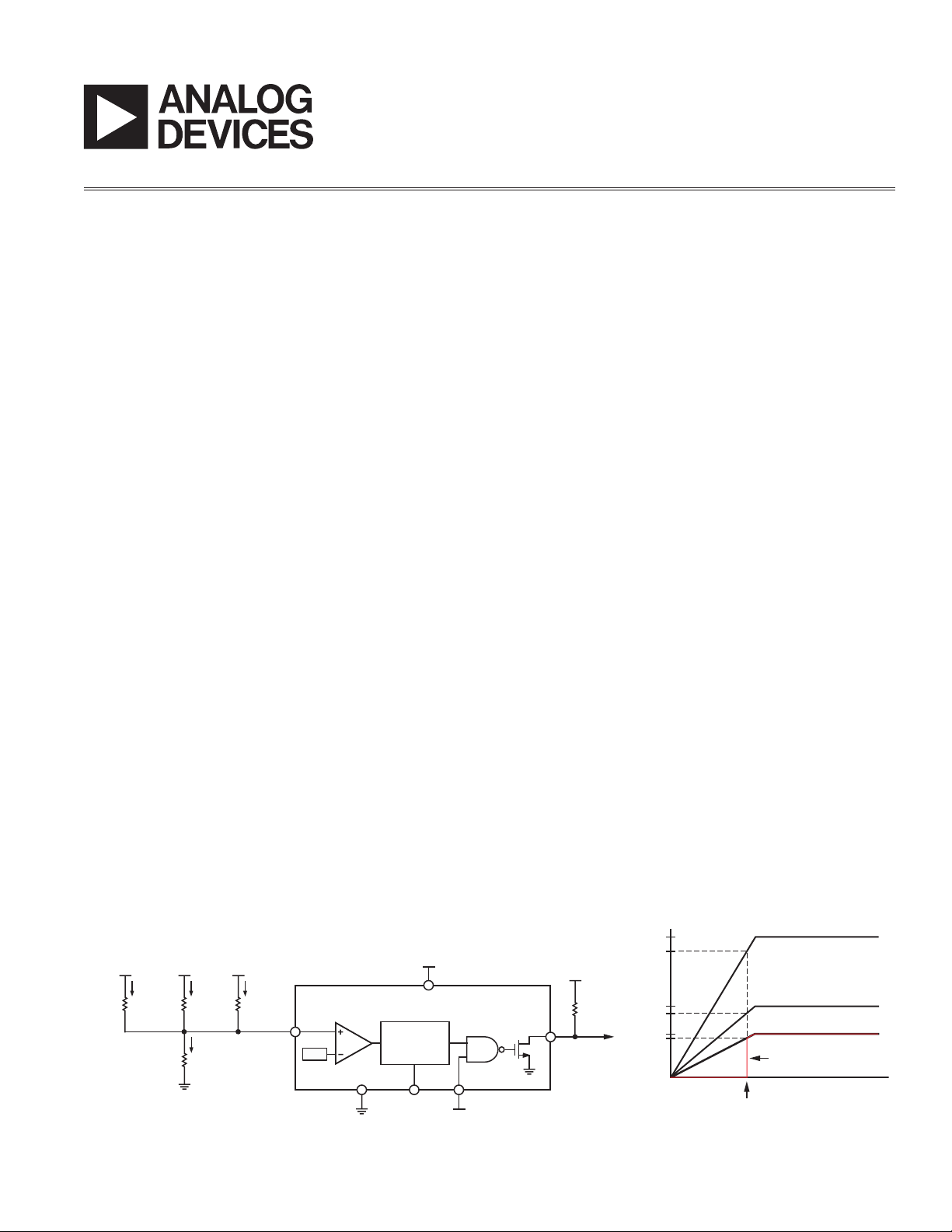
in tolerance. The circuit diagram in Figure 1 is an implementation of such a triple-supply power- good indicator
where the trip points are set at 7% below the nominal
supply level. Resistor values are chosen such that the
comparator input is equal to the ADM1085’s on - chip
voltage reference of 0.6 V when the supplies
trip points of 3.06 V for the 3.3 V supply, 4.65
are at the
V for the 5 V
supply, and 11.16 V for the 12 V supply. The ADM1085’s
CEXT pin is left oating so that power good is asserted
as soon as the comparator switches.
REV. 0
Figure 1. Triple-Supply Monitoring when Supplies Reach Trip Points Simultaneously
Page 2

AN-726
ADM1085
CAPACITOR
ADJUSTABLE
DELAY
0.6V
CEXT
ENIN
V
CC
V
CC
3.3V
POWER_GOOD
3.3V
12V
(9.23V
TRIP POINT)
VIN = 0.6V
8.215A
1.05M
5V
10.81A
407k
3.3V
10.975A
246k
30A
20k
12V
5V
3.3V
COMPARATOR
TRIP POINT
POWER_GOOD
SIGNAL
t
9.23V
t
CEXT
POWER_GOOD
12V
(11.197V
TRIP POINT)
VIN = 0.6V
8.215A
1.29M
5V
10.81A
407k
3.3V
10.975A
246k
30A
20k
12V
5V
3.3V
COMPARATOR
TRIP POINT
POWER_GOOD SIGNAL
t
11.197V
3.3V
ADM1086
STAGGERED POWER-UP
Considering how the same circuit behaves when the
three supplies do not come up simultaneously but in
a staggered fashion, it’s evident that the trip point on
the nal supply to come up will depend on the voltage
levels
at which the other two supplies have settled. Fig-
ure 2 il
lustrates what happens when the 12 V supply is
the last to come up. It is assumed that by the time the
12 V supply has come up, the other two supplies have
powered up and settled at their nominal voltage levels.
As a result, they are injecting more current than if they
had remained at their trip point levels. Since the current
required to give a voltage of 0.6 V across the 20 k re sistor is a
to con
constant, it follows that the 12 V supply needs
tribute less current in order for the comparator to
switch, since both other supplies are contributing more
current. With the 12 V supply sourcing just 8.215 A
instead of 10.057 A for the simultaneous power-up
case, the trip point occurs at 9.23 V rather than 11.16 V.
By using the capacitor adjustable delay feature of the
ADM1085, the premature switching of the comparator
can be compensated for by selecting a suitable time delay so the power- good signal is asserted when all three
supplies have powered up.
KNOWN POWER-UP SEQUENCE
Resistors can be selected to provide a reasonably accurate power- good trip point if the sequence in which the
supplies come up and the values at which they settle is
known beforehand. Figure 3 shows that by adjusting the
12 V supply resistor to 1.29 M , an ADM1086 will assert
the power- good signal when the 3.3 V and 5 V supplies
have settled at their nominal values, and the 12 V supply
reaches 11.197 V, roughly 7% below the nominal supply
value.
AN04858–0–5/04(0)
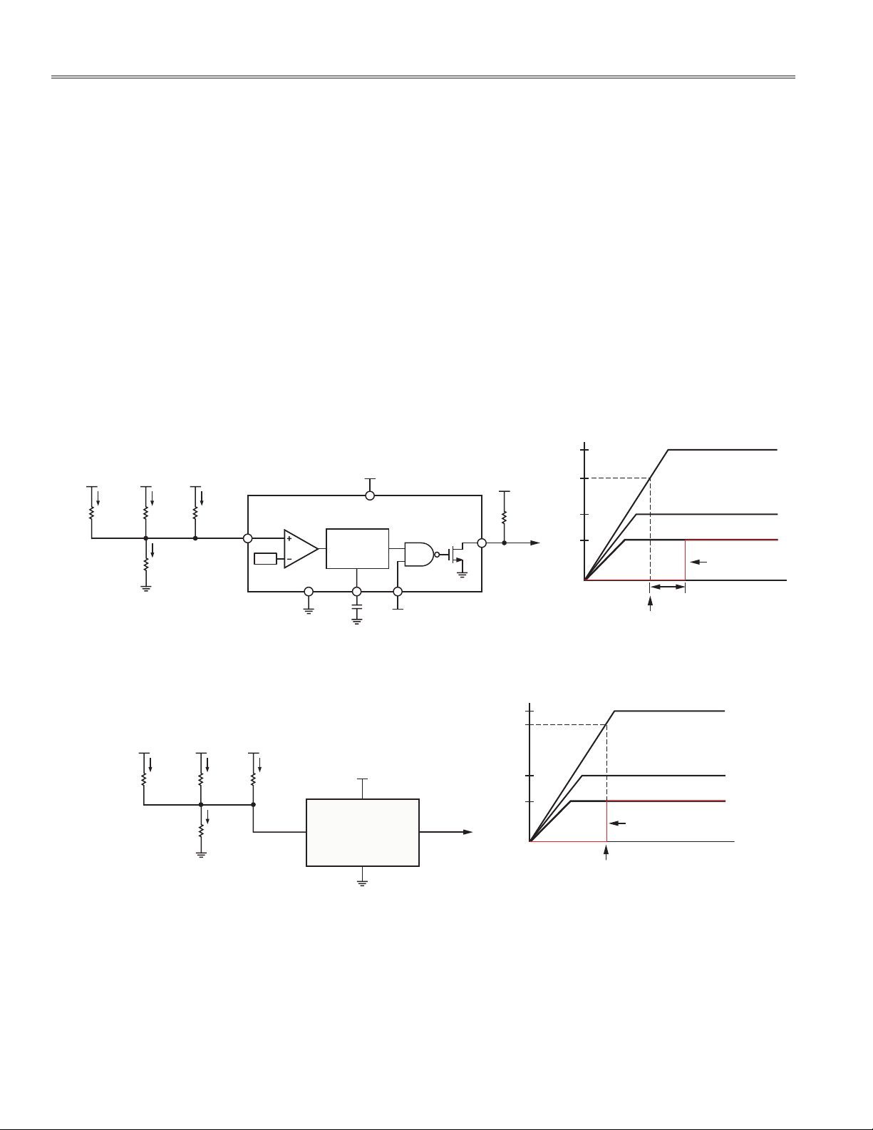
Figure 2. Delayed Power-Good Signal when Power-Up Sequence Is Unknown
Figure 3. Resistor Values Chosen for Desired Trip Point when Power-Up Sequence Is Known
© 2004 Analog Devices, Inc. All rights reserved. Trademarks and registered trademarks are the property of their respective owners.
–2–
REV. 0
 Loading...