

Page 1

AN-705
APPLICATION NOTE
One Technology Way • P.O. Box 9106 • Norwood, MA 02062-9106 • Tel: 781/329-4700 • Fax: 781/326-8703 • www.analog.com
ADN8830-EVAL TEC Controller Instructions
by Troy Murphy
BASIC CONNECTIONS
For basic operation, the TEC+ and TEC– pads on the
right side of the board should be connected to the thermoelectric cooler. The temperature sensing thermistor
must also be connected between the THERMIN and
AGND pads on the left side. Power is applied to VDD at
the top of the board with ground connected to GND. A
minimum of 16- gauge wire is recommended for both
power and ground wires to achieve best effi ciency and
lowest power supply ripple.
No connection is requ ired f or the SD pad because a pullup resistor ensures that the ADN8830 is normally active.
With no output current to the TEC, the board should
draw no more than 15 mA of current. The AGND pad is
a low noise ground and should not return to the power
supply. It is simply a low noise ground reference.
The full schematic for the demo board is given in
Figure 4.
SUPPLY VOLTAGE LIMITS
The maximum supply voltage for the demo board is
5.5 V. The minimum supply voltage is 3.3 V. It is recommended to power the TEC controller from a separate
supply rail from the laser diode supply voltage to minimize noise injection into the laser diode.
The demo board is designed for a maximum sustained
output current of 5.5 A. Although it continues to operate above 5.5 A, performance deteriorates in the form
of lower effi ciency and higher output ripple voltage. The
nominal output ripple voltage using the board’s default
clock frequency of 1 MHz is 10 mV. More information on
output ripple is provided in the ADN8830 data sheet.
ADJUSTING FREQUENCY AND PHASE
The demo board is confi gured to run from its internal
clock at 1 MHz. To change the internal clock frequency,
R5 should be changed according to the instructions in
the ADN8830 data sheet. To drive the ADN8830 from
an external clock connected to SYNCIN, R6 must be
removed. Change R5 to the approximate frequency of
the external clock to ensure that the ADN8830 PLL locks
onto the external clock effectively. The ex ternal clock fre quency must be between 200 kHz and 1 MHz for proper
synchronization to occur.
The default phase shift on the board is approximately
135 and is set by the voltage dividers R2 and R4. Dif fer-
ent phase shifts can be set by adjusting these resistors
according to the ADN8830 data sheet.
ADJUSTING MAXIMUM TEC VOLTAGE
The demo board comes confi gured with the VLIM pin
pulled to ground through 100 k resistor R16. This
deactivates the output voltage limiting and allows
the TEC voltage to swing to the supply rails. To set a
lower maximum output voltage across the TEC, apply a
voltage to the VLIM pad according to the ADN8830 data
sheet. This voltage is easily set with a resistive voltage
divider, a voltage source, or a DAC.
The ADN8830 demo board is normally active, but can be
shut down by applying a logic low voltage to the SD pad.
This pin is pulled to VDD through a 100 k resistor, so a
connection to this pad is not required.
ADJUSTING TEMPSET
The TEMPSET voltage is set on the board through resis tors R10 and R11. Using a 10 k thermistor connected,
the default TEMPSET voltage is set for a 25 C set point.
A DAC can be easily connected to the TEMPSET pad to
change the target temperature. If a DAC is used, it is
important to connect its full -scale reference voltage to
VREF from the demo board. This ensures the best resolution for target temperature.
REV. 0
Page 2
AN-705
–3–
AN-705
POWER SUPPLY
VDD GND
ADN8830-EVAL
VDD GND
TEC
A
V
A
V
ITEC (mA)
EFFICIENCY (%)
100
80
60
20
40
0
0 500 1000 1500 2000
VSY = 3.3V
VSY = 5.0V
REV. 0
When using the components on the demo board, and
a laser diode module standard 10 k thermistor with a
0/ 50 Beta value of 3892 (Alpha value of –4.39% at 25C),
use the following voltage table:
Table I. TEMPSET Voltages and Binary Codes Corresponding
to Target Temperatures
Target TEMPSET
Temp Voltage 12-Bit Code 10-Bit Code
5C 1.8811 V 110001001010 1100010011
10C 1.7581 V 101101111011 1011011111
15C 1.6340 V 101010101100 1010101011
20C 1.5099 V 100111011100 1001110111
25C 1.3857 V 100100001101 1001000011
30C 1.2616 V 100000111110 1000001111
35C 1.1375 V 011101101111 0111011011
40C 1.0134 V 011010011110 0110100111
45C 0.8881 V 010111001110 0101110011
Exact equations for alternative temperatures can be
found in the ADN8830 data sheet.
The R7 value of 7.68 k is selected for minimum temperature-to-voltage error across a temperature range of
5C to 45C, using the 10 k thermistor specied previously. For an alternate temperature range or thermistor
type, refer to the applications section in the ADN8830
data sheet to optimize R7. The VREF value used for
calculation is 2.45 V.
ADJUSTING COMPENSATION LOOP
A compensation network is provided on the ADN8830
demo b oar d to f acilit ate t he dev ice’s performance.
Although this network may not have the optimum settling time for the particular laser module, it is stable
across a wide range of laser modules. Settling within
0.1 C should occur within several seconds, depending
on the temperature change step size and the laser power
being dissipated, and is indicated by the green LED.
If the demo board does not settle to a xed temperature,
or an oscillation on the output voltage is obser ved,
the compensation network needs to be adjusted. The
simplest method for ensuring stability is to reduce the
bandwidth of the compensation network, by increasing
the integration capacitor C20. The trade- off is an increase
in settling time, which may be required based on the laser
module being controlled. Additional details on adjusting
the compensation loop are given in the data sheet.
READING TEMPOUT AND VTEC
The ADN8830 TEMPOUT and VTEC pins can be read
directly from their respective pads on the demo board.
For more information on these outputs, refer to the
ADN8830 data sheet.
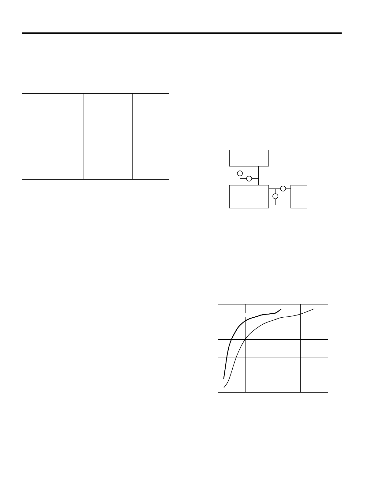
EFFICIENCY MEASUREMENTS
With 1 A of constant output current from a 3.3 V supply,
the efciency of the ADN8830 demo board is measured
at 90% . At lower clock frequencies, efciency improves
to 94% . To measure efciency manually, simultaneously
measure the exact supply current, supply voltage, TEC
current, and TEC voltage. Use a low resistance ammeter for
accurate measurements in the following conguration:
Figure 1. Measuring Efciency of the ADN8830
Demo Board
Output power is the output voltage multiplied by TEC
current; supply power is supply voltage multiplied by
supply current. The efciency of the system is simply
output power divided by supply power. It is important
to subtract 6 mA from the supply current measurement
because that is the current through the green Temp
Good LED when it is on, and is not currently used by
the ADN8830 itself. Figures 2 and 3 show the measured
efciency of the demo board.
Figure 2. Efciency Measurements with 1 MHz
Switching Frequency
–2–
REV. 0
Page 3

ITEC (mA)
EFFICIENCY (%)
100
80
60
20
40
0
0 500 1000 1500 2000
VSY = 3.3V
VSY = 5.0V
Figure 3. Efciency Measurements with 220 kHz
R8
1k
R6
0
C5
100nF
C9
1nF
C13
10nF
C15
10nF
C21
330pF
C22
3.3nF
C8
0.1F
C23
1F
C18
0.1F
C12
1F
C7
0.1F
C16
22F
C20
10F
C10
0.1F
4.7H
COILCRAFT
DO3316P-472
Q2
FDW2520C-B
Q1
FDW2520C-A
Q3
FDW2520C-B
Q4
FDW2520C-A
C6
22F
CDE ESRD
AVDD
L1
TEC–
TEC+
PVDD
PVDD
PVDD
24
23
22
21
20
19
18
17
32 31 30 29 28 27
TEMPOUT
D2
TEMP GOOD
GREEN
DIALIGHT
597-7701-102
THERM FAULT
RED
DIALIGHT
597-7701-102
D1
Q6
FDV301N
Q5
FDV301N
R2
332k
R13
205k
R15
1M
TEMPCTL COMPIN COMPOUT VLIM VTEC
R16
100k
R14
100k
R4
196k
R1
499
R3
100k
R5
150k
C1
10nF
C2
1F
VREF
U1
ADN8830
AVDD
AVDD PVDD
VDD
VREF
TEMPSET
SD
SYNCIN
SYNCOUT
26 25
C24
22F
CDE ESRD
C3
22F
CDE ESRD
C25
22F
C26
22F
PVDD
9 10 11 12 13 14 15 16
R11
7.68k
0.1%
R9
100k
R10
10k
0.1%
R7
7.68k
0.1%
R12
499
1
2
3
4
5
6
7
8
C4
0.1F
AVDD
AVDD
THERMINGROUND
C19
2.2nF
Switching Frequency
AN-705
BOARD LAYOUT AND COMPONENT SELECTION
Figure 4 shows the complete demo board schematic.
The board consists of four layers, including ground and
power planes as shown in Figures 5 to 10. Circles in
the drill guide in Figure 10 represent 10 mil via holes;
squares represent 20 mil vias.
Both power and ground planes are split into two sections
to separate switched output currents from low noise
analog currents required by the input stage. Note the
symmetry of the power and ground planes; this minimizes
current ow path and resultant parasitic inductance of
high frequency currents, which, in turn, reduces ground
and power supply bounce.
The PWM output transistors and components are contained in the upper right area of the board to minimize
trace resistances and potential switched noise injection
into other traces.
REV. 0
Figure 4. ADN8830-EVAL Schematic
–3–
Page 4

AN-705
AN04643–0–3/04(0)
Figure 5. Top Overlay
Figure 6. Top Layer
Figure 8. Ground Plane
Figure 9. Bottom Layer
Figure 7. Power Plane
© 2004 Analog Devices, Inc. All rights reserved. Trademarks and registered trademarks are the property of their respective owners.
–4–
Figure 10. Drill Guide
REV. 0
 Loading...