

Page 1

AN-703
Preliminary Technical Data
APPLICATION NOTE
One Technology Way • P.O. Box 9106 • Norwood, MA 02062-9106 • Tel: 781/329-4700 • Fax: 781/326-8703 • www.analog.com
Driving High Power LEDs
by Yuxin Li, Gang Liu, and Alan Li
INTRODUCTION
The ADP3806 is a switching mode power supply (SMPS)
controller featuring dual loop constant-voltage and
constant-current control; remote and accurate current
sensing; and shutdown and programmable, synchronizable switching frequency. For different application
requirements, it can be confi gured in a variety of topologies:
buck, boost, buck-boost, SEPIC, and CUK. This application
note guides the designs of controller circuits for driving
high power LEDs (light emitting diodes) by using the
ADP3806 to achieve an effi ciency of up to 95%.
Before using this application note for designing the circuits, download the ADP3806 data sheet from the ADI
website.
POWERING UP THE ADP3806
The minimum VCC is 6.25 V (undervoltage lockout UVLO
voltage) and the maximum VCC should not exceed 23 V,
which brings the switch driver voltage BST to 30 V, the
junction breakdown voltage. The recommended VCC
range is from 6.5 V to 20 V.
To e n s u r e a clean voltage source at the VCC pin, an RC
bypass network is used between the input source and
the IC. The decoupling capacitor can be in the value
range of 0.1 F to 22 F. The sh u tdown control pin SD
accepts external control logic input. If automatic startup
is preferred, a voltage divider from VCC can be used to
ensure that the voltage at this pin is below its limit, 10 V,
and above its logic high, 2.0 V.
A capacitor connected to the CT pin sets the switching
frequency. Recommended switching frequency is from
300 kHz to 750 kHz for the optimized trade-off between
the overall system physical size and the efficiency.
Higher switching frequency of up to 1 MHz demands
more gate-driving power and generates more switching
losses, resulting in lower effi ciency, while the inductors’
inductance can be scaled down to reduce the system’s
physical size and cost. Another drawback of using a
higher switching frequency is that the duty cycle range is
reduced so that the output voltage range is narrowed.
REG, REF, and BSTREG pins are output pins of three internal low dropout (LDO) regulators. Decouple them with
the recommended capacitors to ensure the stability of
the regulators.
The current sensing resistor along with the voltage at
the ISET pin determines the output current. The required
voltage at the ISET pin should be generated from the
2.5 V precision reference source REF pin. The maximum
output current from the REF pin is 500 A. To generate
a higher setting voltage, the voltage divider can run off
the REG pin (6 V). Note that the accuracy for REF is 1%,
and the accuracy for REG is 3%.
Across CS+ and CS– pins, a fi lter capacitor of about 220 nF
should be placed right next to the pins in the PCB layout
to fi lter out noise.
BUCK CONFIGURATION
To d rive L EDs w ith an output voltage lower than the input
power source voltage, a step-down topology Buck can
be used.
Figure 1 shows the Buck configuration circuit. This
scheme utilizes the synchronous rectification functionality of the controller to provide the highest power
conversion effi ciency. The controller and the power
stage can be powered up by either the same or different power sources. Using the same power source, the
input voltage range should be within the range of 6.5 V
to 20 V. With different power sources, the power stage
input voltage can be as low as 6.5 V, while the maximum
should not exceed 20 V.
Using proper MOSFETs, the output current can go up to
4 A, the sense resistor value, and the ISET voltage. The
output voltage can go from zero up to the power stage
input voltage.
The current sensing resistor, R
to minimize its power loss but high enough to provide
suffi cient signal for the control. The voltage across the
CS+ and CS– pins should be higher than 50 mV to activate
the synchronous rectifi cation function, that is, to switch
the lower MOSFET on and off. When (CS+ – CS–) voltage
is lower than 50 mV, the low-side MOSFET is not turned
on so its body diode conducts, causing extra conduction
loss. At the same time, the energy for driving the lower
MOSFET is saved. When the output current is lowered
far enough, turning off the lower MOSFET may result in
higher overall system effi ciency.
, should be low enough
CS
REV. PrA
Page 2

AN-703 Preliminary Technical Data
By using the circuit shown in Figure 1, the output current
equals
V
I
LED
ISET
=
R
25
CS
If the current sensing signal in the design is lower than
50 mV, a bias circuit, shown in Figure 2, is needed to fully
activate the synchronous functionality. By using a voltage
divider composed of RB1 and RB2, a bias voltage, V
BIAS
, is
generated at the CS+ pin. Thus, the sensing signal needed
to activate the synchronous rectifi cation function is V
lower than the 50 mV. If V
equals 50 mV, the synchro-
BIAS
BIAS
nous function is effective all the time. With this bias, the
output current is
VV
- 25
LED
=
ISET BIAS
R
25
CS
I
The current limit setting accuracy is obviously a little
lower with this added offset term. Also, the biasing
circuitry should draw minimum current from the VREF
pin, and fi ltering capacitor C4 should now be designed
to make a small enough time constant (recommend 0.3/
f
) with RB2 instead of RCS. Thus, C4 is much smaller
SW
than 200 nF.
The output capacitor, C
, is optional. It smoothes the
OUT
voltage and current across the LEDs.
The input capacitor, C
, is needed to absorb the input ripple
IN
current. Normally, two 10 F/25 V ceramic capacitors are
enough.
The inductor, L, determines the ripple current. It is recommended that the ripple current be about one-third of the
nominal output current to optimize both the system size
and the effi ciency. The peak inductor current is there
II
= 115.
LPEAK LEDM
fore,
where:
is the peak current of the inductor.
I
LPEAK
is the maximum average current in the LEDs.
I
LEDM
The inductor should be chosen based on two criteria.
First, the inductor saturation current should be larger
than the maximum peak current, I
, in the inductor.
LPEAK
Second, the inductor’s maximum dc current rating should
be larger than the load dc average current, I
LED
.
The recommended bootstrap capacitance is 10 nF. A
0.5 A Schottky diode is recommended as the bootstrap
diode. This diode must be placed on the PCB as close to
the BST and BSTREG pins as possible.
C
, CCL, and RC compose the loop compensation net-
CH
work of the closed loop. They need to be designed
carefully to ensure system stability and control speed.
The control (duty cycle, d) to inductor current (i
) transfer
L
function is a constant given by
iS
()
L
d
=
25
DV
IN
Rf L
CS SW
where:
D is the duty cycle of the steady state.
is the switching frequency of the power stage.
f
SW
This is valid below half of the switching frequency and
with the assumption that the output voltage is constant.
It is obvious that a simple integrator is adequate to compensate the loop with infi nite dc gain. To set a bandwidth
of f
), the compensation component CCL needs to be
C(C
gDV
C
CL
MIN
=
Rf L
25 w
CS SW C
where:
= 0.002 is the transconductance of the current loop
g
M
error amplifi er.
R
can be set to zero.
C
can be set to be open.
C
CH
LEDs are not critical to the driving transition, so the system loop bandwidth can be low. It is recommended that
the bandwidth is designed to be 1/30th of the switching
frequency for the buck confi guration.
MOSFETs can be chosen based on their dc voltage/
current ratings, switching speed (gate charges), and
thermal capability.
Note that the BSTREG regulator needs to provide the
entire gate-driving energy to drive both the high-side
MOSFET and the high- side driver itself. Because the
maximum output current, I
lator is ⱕ 3 mA, the gate charge, Q
, of the BSTREG regu -
BSTREG
, of the high-side
G
MOSFET and the switching frequency should satisfy
IQf
>
BSTREG G SW
If more gate-driving capability is needed, use an external
NPN transistor, QBST, in the emitter follower confi guration (see Figure 2) to deliver more current.
–2–
REV. PrA
Page 3
Preliminary Technical Data AN-703
VIN7V–20V
C1
R1
22F
10⍀
124
VCC
2
R2
100k⍀
CT
C2
100nF
C3
200pF
R3
51k⍀
C
CL
R
C
C
CH
SYS–
3
SYS+
4
ISYS
5
LIMIT
6
CT
7
8
9
10
11
12
ADP3806
SYNC
REG
REF
SD
COMP
LC AGND
SW
DRVH
BST
BSTREG
DRVL
PGND
CS+
CS–
ISET
BATSEL
BAT
C6
23
22
21
20
19
18
17
16
15
14
13
10nF
D1
MBR052
C5
1F
C4
200nF
TO SET THE OUTPUT CURRENT
R
CLBRCLT
SW1
SW2
C
IN
L
V
OUT
=0TOV
IN
LED1
C
OUT
LED2
R
CS
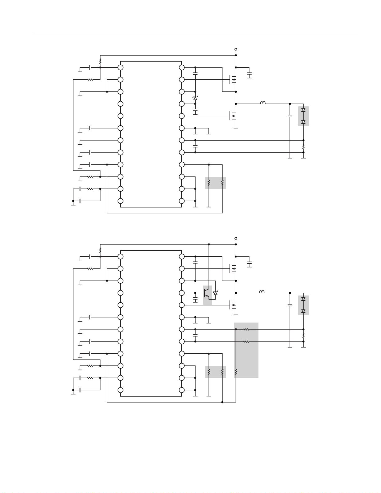
Figure 1. Driving LEDs with the ADP3806 in Buck Confi guration
VIN7V–20V
C1
R1
22F
10⍀
124
VCC
2
R2
100k⍀
CT
C2
100nF
C3
200pF
R3
51k⍀
C
CL
R
C
C
CH
SYS–
3
SYS+
4
ISYS
5
LIMIT
6
CT
7
8
9
10
11
12
ADP3806
SYNC
REG
REF
SD
COMP
LC AGND
SW
DRVH
BST
BSTREG
DRVL
PGND
CS+
CS–
ISET
BATSEL
BAT
C6
23
22
21
20
19
18
17
16
15
14
13
10nF
QBST
BBMT6428
C5
1F
OUTPUT
CURRENT BOOSTER
C4
??
TO SET THE
OUTPUT CURRENT
D1
MBR052
R
CLBRCLT
C
IN
SW1
L
SW2
C
RB2
RB3
RB1
CURRENT SENSING BIAS
OUT
V
OUT
=0TOV
R
CS
IN
LED1
LED2
REV. PrA
Figure 2. Biasing the Current Sensing Input to Accommodate Low Input Signal
–3–
Page 4

AN-703 Preliminary Technical Data
BOOST CONFIGURATION
If the output voltage is higher than the input power
source voltage to power a series of LEDs, step-up conversion is used.
Figure 3 shows the boost confi guration using the ADP3806
to drive LEDs. This scheme utilizes the main driving output DRVH to control the main switch SW1, with the diode
switch SW2 used for rectifi cation.
To a v oid ov e r voltage output, the voltage loop can be
connected to set the maximum allowable output voltage, V
. Because the internal reference is 2.5 V, the
OUTM
maximum output voltage is set by
RR
=+25.
OVPT OVPB
R
OVPB
V
OUTM
Choose appropriate voltage divider resistance to set the
overvoltage protection point, V
C1
R1
22F
10⍀
R2
100k⍀
CT
C2
100nF
C3
200pF
51k⍀
R3
C
CL
R
C
C
CH
.
OUTM
124
VCC
2
SYS–
3
SYS+
4
ISYS
5
LIMIT
6
CT
7
8
9
10
11
12
ADP3806
SYNC
REG
REF
SD
COMP
LC AGND
SW
DRVH
BST
BSTREG
DRVL
PGND
CS+
CS–
ISET
BATSEL
BAT
23
22
21
20
19
18
17
16
15
14
13
The output capacitor, C
, is optional. Without it, the
OUT
current fl owing into the LEDs is discontinuous and fl uctuates at a duty of (1 – D), where D is the duty cycle of
the PWM control. With the output capacitor, the current
in the LEDs can be shaped smoother. Appropriate output
capacitance is needed to achieve the required driving
current pattern.
The current sensing resistor, R
, needs to be large
CS
enough to generate suffi cient signal for the controller.
The maximum differential input voltage between CS+
and CS– is 160 mV.
C
, CCL, and RC need to be designed carefully to ensure
CH
system stability and control speed. This design is different
from that of the buck confi guration.
With this confi guration, the output is always connected
to the input power supply via SW2 and the inductor, even
when the controller is in shutdown mode. This may pose
some issues for specifi c applications.
VIN2VIN1 7V–20V
C
IN
L
C5
1F
C4
200nF
TO SET THE
OUTPUT CURRENT
R
OVPBRCLBRCLT
SW2
SW1
R
OVPT
TO SET THE MAXIMUM
OUTPUT VOLTAGE
C
V
OUT
OUT=VIN
+1AND UP
LED1
LED2
R
CS
Figure 3. Driving LEDs with the ADP3806 in Boost Confi guration
–4–
REV. PrA
Page 5

Preliminary Technical Data AN-703
SEPIC CONFIGURATION
The SEPIC confi guration provides an output that can be
either higher or lower than the input voltage at a cost
of an additional inductor and capacitor. A SEPIC confi guration using the ADP3806 to drive LEDs is shown in
Figure 4.
The output stage is very similar to the boost confi guration, except that the rectifi cation switch, SW2, conducts
when the main switch, SW1, is on.
C1
R1
22F
10⍀
124
VCC
2
R2
100k⍀
CT
C2
100nF
C3
200pF
51k⍀
R3
C
CL
R
C
C
CH
SYS–
3
SYS+
4
ISYS
5
LIMIT
6
CT
7
8
9
10
11
12
ADP3806
SYNC
REG
REF
SD
COMP
LC AGND
SW
DRVH
BST
BSTREG
DRVL
PGND
CS+
CS–
ISET
BATSEL
BAT
23
22
21
20
19
18
17
16
15
14
13
The output capacitor, C
, CCL, and RC need to be designed carefully to ensure
C
CH
, is optional.
OUT
system stability and control speed. This design is different
from that of the buck confi guration.
Unlike the boost confi guration, the output is isolated to the
input source when the controller is in shutdown mode.
VIN2VIN1 7V–20V
C
IN
L1
C
C5
1F
C4
200n
TO SET THE
OUTPUT CURRENT
R
OVPBRCLBRCLT
R
SW1
R
TO SET THE MAXIMUM
OUTPUT VOLTAGE
OVPT
SW2
L2
C
OUT
V
OUT
LED1
LED2
R
CS
REV. PrA
Figure 4. Driving LEDs with the ADP3806 in the SEPIC Confi guration
–5–
Page 6

AN-703 Preliminary Technical Data
CUK CONFIGURATION
The CUK confi guration provides an inverted output that
can be either higher or lower in magnitude than the input
voltage. Figure 5 shows the CUK confi guration using the
ADP3806 to drive LEDs.
Similar to the buck confi guration, the output current is
continuous, with fewer pulsating components compared
to both the boost and the SEPIC confi gurations.
C1
R1
22F
10⍀
124
VCC
2
R2
100k⍀
CT
C2
100nF
C3
200pF
51k⍀
R3
C
CL
R
C
C
CH
SYS–
3
SYS+
4
ISYS
5
LIMIT
6
CT
7
8
9
10
11
12
ADP3806
SYNC
REG
REF
SD
COMP
LC AGND
SW
DRVH
BST
BSTREG
DRVL
PGND
CS+
CS–
ISET
BATSEL
BAT
23
22
21
20
19
18
17
16
15
14
13
Similarly, the output capacitor, C
, CCL, and RC need to be designed carefully to ensure
C
CH
, is optional.
OUT
system stability and control speed. This design is different
from that of the buck confi guration.
The output is isolated to the input source when the
controller is in shutdown mode.
VIN2VIN1 7-20V
C
IN
L1
CR
C5
1F
C4
200nF
TO SET THE OUTPUT CURRENT
R
CLBRCLT
SW1
SW2
L2
C
OUT
V
OUT
LED1
LED2
R
CS
Figure 5. Driving LEDs with the ADP3806 in the CUK Confi guration
–6–
REV. PrA
Page 7

Preliminary Technical Data AN-703
BRIGHTNESS CONTROL
Brightness control can be implemented easily by controlling the voltage at Pin ISET. Referring to the data sheet,
the output current, I
, is set by V
OUT
(voltage at the ISET
ISET
pin) by
V
I
OUT
ISET
=
R
25
CS
There are two basic ways to adjust the brightness control. The fi rst is to control the output current by changing
V
at the ISET pin. This can be done simply by using a
ISET
potentiometer running off the 6 V V
rail or 2.5 V V
REG
REF
reference.
To minimize the board space, layout infl exibility, and
reliability concern, users may consider using a digital
potentiometer, AD5228, rather than its mechanical
counterpart for the brightness control. AD5228 is a low
cost, 32-step, manual control digital potentiometer that
features a built-in debouncer and zero-scale/midscale
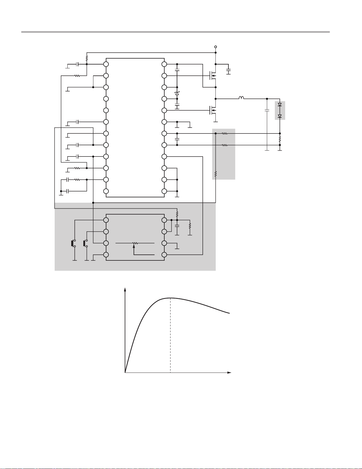
selectable preset. As shown in Figure 6, an AD5228 with
two external push buttons adds in the circuit fl exibility
with brightness control.
This control is simple but may be ineffi cient because
the effi ciency of LEDs tends to be higher at their full cur-
rent rating and lower at reduced current. To overcome
this problem, a PWM brightness control scheme can be
used.
By periodically shorting the ISET pin down to AGND,
V
shows a pattern of PWM, as does the output cur-
ISET
rent, I
. With an open-drain MOSFET connected to the
OUT
ISET pin, the brightness of the output can be controlled
by a digital signal, which can be generated by a micro controller.
It takes time for the controller to react to the control
signal, so the frequency of this brightness control PWM
signal should be much lower than the bandwidth of the
control loop, which is much slower than the switching
frequency. The brightness PWM signal can be in the
range of 50 Hz to 500 Hz.
Figure 7 shows a typical high brightness LED’s effi ciency
curve versus its driving current. I
is the optimal driving
OPT
current point with the highest light emitting effi ciency.
The effi ciency optimized brightness control approach is
to drive the LEDs with a PWM current pattern. The current changes from zero to I
at a duty D
OPT
. This leads
BRI
to the maximum light-emitting output at the continuous
I
driving. Whe n more lig ht output is needed, raise the
OPT
driving current.
REV. PrA
–7–
Page 8
AN-703 Preliminary Technical Data
VIN7V–20V
C1
R1
22F
10⍀
124
VCC
2
R2
100k⍀
SYS–
3
SYS+
4
ISYS
5
LIMIT
CT
6
CT
C2
100nF
C3
200pF
51k⍀
R3
C
CL
R
C
C
CH
7
8
9
10
11
12
ADP3806
SYNC
REG
REF
SD
COMP
LC AGND
SW
DRVH
BST
BSTREG
DRVL
PGND
CS+
CS–
ISET
BATSEL
BAT
C6
23
22
21
20
10nF
D1
MBR052
C5
1F
SW1
SW2
C
IN
L
V
OUT
=0TOV
IN
LED1
C
OUT
LED2
19
18
17
16
15
14
13
C4
200nF
RB2
RB3
RB1
CURRENT SENSING BIAS
R
CS
PR04631–0–3/04(PrA)
PUSH-UP BUTTON
PUSH-DOWN BUTTON
OUTPUT CURRENT SETTING
Figure 6. Brightness Control Using AD5228 Manual Control Digital Potentiometer
RB1
124
PU
PD
A
GND
ADP5228
2
3
4
VDD
PRE
B
W
1k⍀
RB2
10k⍀
CB
23
100nF
22
21
LIGHT EMITTING EFFICIENCY
I
LED DRIVING CURRENT
OPT
Figure 7. Typical High Brightness LED’s Effi ciency
© 2004 Analog Devices, Inc. All rights reserved. Trademarks and registered trademarks are the property of their respective owners.
–8–
REV. PrA
 Loading...