

Page 1
AN-698
CLOSED LOOP
MARGINING SYSTEM
DU
AL
FUNCTION
INPUTS
(LOGIC
INPUTS
OR SFDs)
PROGRAMMABLE
RESET
GENERA
TORS
(SFDs)
CONFIGURABLE
OUTPUT
DRIVERS
(HV-CAPABLE
OF DRIVING
GATE OF
N-CHANNEL
FET)
CONFIGURABLE
OUTPUT
DRIVERS
(L
V-CAPABLE
OF DRIVING
LOGIC
SIGNALS)
V
OUT
DAC
V
OUT
DAC
V
OUT
DAC
V
OUT
DAC
V
OUT
DAC
V
OUT
DAC
ADM1066
EEPROM
VDD
ARBITRATO
R
SEQUENCING
ENGINE
VX1
VX2
VX3
VX4
VX5
VP1
VP2
VP3
VP4
VH
SFDGND
DAC
1 DAC2 DAC3 DAC4 DAC5 DAC6 GND
VDDCAP
PDOGND
PDO10
PDO9
PDO8
PDO7
PDO6
PDO5
PDO4
PDO3
PDO2
PDO1
AUX1 AUX2 REFIN REFGND SD
A SCL A1 A0REFOUT
MUX
12-BIT
SAR ADC
SMBUS
INTERFAC
E
V
REF
APPLICATION NOTE
One Technology Way • P.O. Box 9106 • Norwood, MA 02062-9106 • Tel: 781/329-4700 • Fax: 781/326-8703 • www.analog.com
Conguration Registers of ADM106x
by Peter Canty
INTRODUCTION
The ADM106x family of fully programmable supply
sequencers and supervisors can be used as complete
supply management solutions in systems using multiple
voltage supplies. Such applications include line cards in
telecommunications infrastructure equipment (central
ofce, base stations) and blade cards in servers.
All of the features of the ADM106x are programmable
through an SMBus interface. The devices also contain
nonvolatile memory (EEPROM) so that the conguration
of these features can be stored on-chip and downloaded
each time on power-up.
This application note briefly outlines the func tions of
the ADM106x, and provides details of the registers
required to set up the conguration of the ADM106x.
The programming windows of the ADM106x graphical
user interface (GUI) based software provided by ADI to
congure these devices is also shown.
For more information on the features and functions of
the ADM106x, please refer to the relevant data sheet.
REV. 0
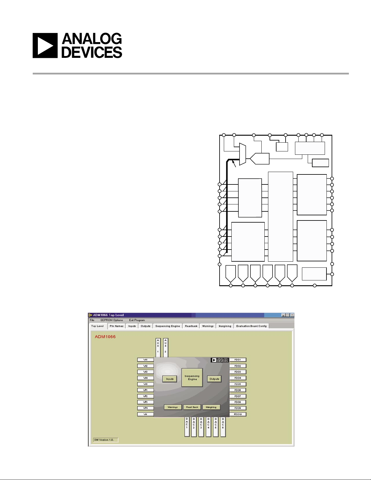
Figure 1. ADM1066 Functional Block Diagram
Figure 2. Top Level Menu of ADM106x Software
Page 2
AN-698
–3–
AN-698
POWER-UP
VCC >2.5V
EEPROM
E
E
P
R
O
M
L
D
DEVICE
CONTROLLER
SMBus
LATCH A
D
A
T
A
LATCH B
R
A
M
L
D
U
P
D
FUNCTION (eg)
OV
THRESHOLD
ON VP 1
REV. 0
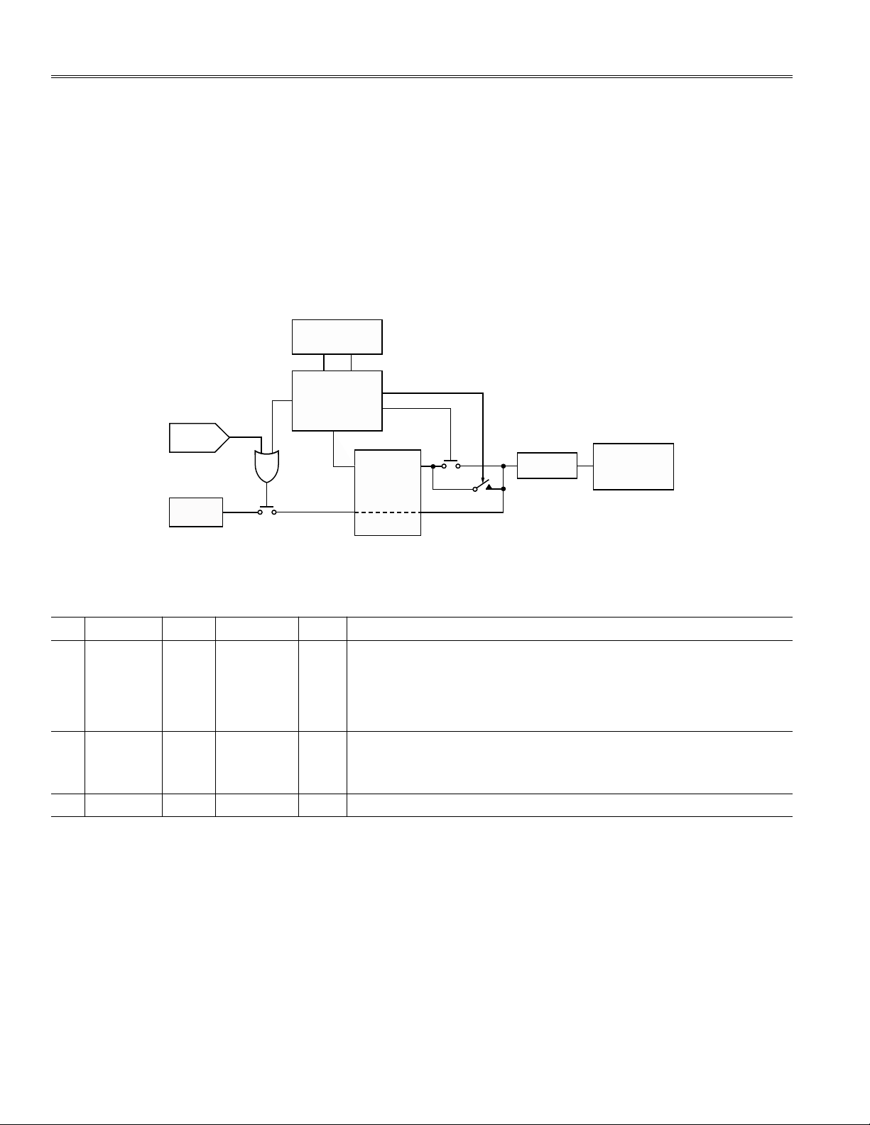
UPDATING THE ADM106x
The following pages contain all of the register information required to congure the many features of the
ADM106x. The ADM106x contains both volatile and nonvolatile memory, which must be set up correctly if any
alterations to the conguration are to be updated prop erly in the device. The volatile memory of the ADM106x is
constructed with double buffered latches. For information
on this construction, please refer to the data sheet.
The register/bit map detail below shows the congura tion required to
• Update volatile memory in real time.
• Update volatile memory off line then update
all at once.
• Enable block erase.
• Download EEPROM contents to RAM.
The sequencing engine also has a number of conguration
bits that are used to update it and are detailed below.
Figure 3. Conguration Update Flow Diagram
Table I.
Reg. Reg. Name Bits Bit Name R/W Description
90H UPDCFG 7:3 Cannot be used.
2 EEBLKERS R/W Enable conguration EEPROM Block Erase.
1 CFGUPD W Update conguration registers from holding registers (self clears).
0 CONTUPD R/W Enable continuous update of conguration registers.
D8H UDOWNLD 7:1 Cannot be used.
0 EEDWNLD W
Download conguration data from EEPROM. This also happens automatically
at power-up. Self clears on completion.
F4 MANID 7:0 R Manufacturer’s ID, returns 0x41. Good method of verifying communication.
–2–
REV. 0
Page 3
AN-698
ADM106x INPUTS
The ADM106x devices have 10 inputs. Five of these are
dedicated supply fault detectors—highly programmable
reset generators whose inputs can detect overvoltage,
undervoltage, or out- of- window faults. With these ve
inputs, voltages from 0.573 V to 14.4 V can be supervised. The undervoltage and overvoltage thresholds can
all be programmed to 8- bit resolution. The comparators
used to detect faults on the inputs have digitally pro grammable hysteresis to provide immunity to supply
bounce. Each of these inputs also has a glitch lter
whose timeout is programmable up to 100 µs.
The other ve inputs have dual functionality. They can
be used as analog inputs, like the rst ve channels
de
scribed above, or as general - purpose logic inputs. As
analog inputs, these channels function exactly the same
as those described above. The major difference is that
these inputs do not have internal potentiometer resistors
and present a true high impedance to the input pin. Their
input range is thus limited to 0.573 V to 1.375 V, but the
high impedance means that an external resistor divide
network can be used to divide down any out- of-range
sup
ply
to a value within range. Thus, +48 V, +24 V, –5 V,
and –12 V can all be supervised by these channels with
the appropriate ex ternal resistor network.
As digital inputs, these pins can be used to detect enable
signals, PWRGD, POWRON, and so on. They are TTL and
CMOS compatible. When used in this mode, the analog
circuitry of these pins can be mapped to its sister input
pin (one of the rst ve inputs described above). Thus,
VX1 can be used as a second detector on VP1, VX2 can
be used with VP2, and so on. VX5 is mapped to VH.
With a second detector available, the user can program
ALARM as well as fault functions.
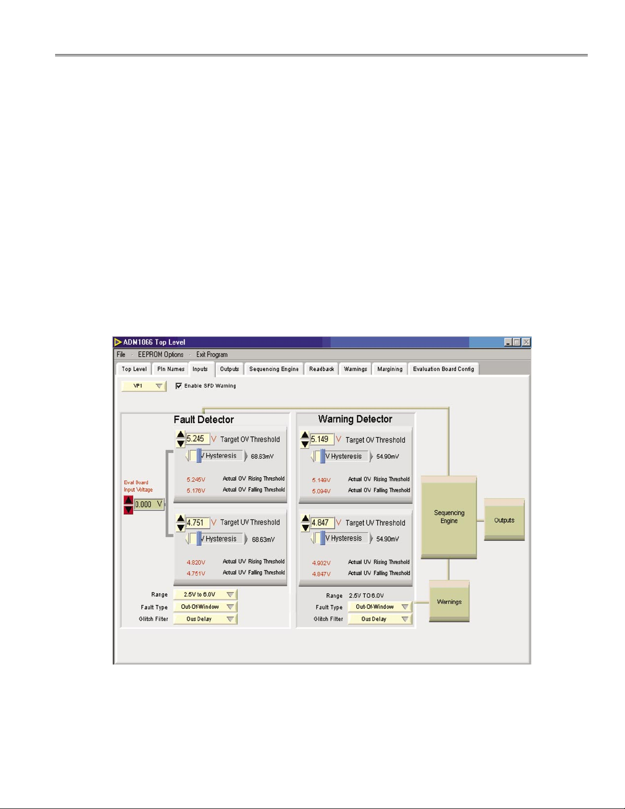
Figure 4 shows the GUI window for conguring the
inputs. Table II details all of the registers used to con-
gure the inputs to perform the functions described
above.
REV. 0
Figure 4. ADM106x Inputs Window
–3–
Page 4

AN-698
–5–
AN-698
REV. 0
Table II.
Input Reg. Reg. Name Bits Bit Name R/W Description
VP1 00H PS1OVTH 7:0 OV7–OV0 R/W 8-bit digital value for OV threshold on PS1 SFD.
01H PS1OVHYST 7:5 Cannot be used.
4:0 HY4–HY0 R/W 5-bit hysteresis to be subtracted from PS1OVTH when OV is true.
02H PS1UVTH 7:0 UV7–UV0 R/W 8-bit digital value for UV threshold on PS1 SFD.
03H PS1UVHYST 7:5 Cannot be used.
4:0 5-bit hysteresis to be added from PS1UVTH when UV is true.
04H SFDV1CFG 7:5 Cannot be used.
4:2 GF2–GF0 R/W GF2 GF1 GF0 Delay (µs)
0 0 0 0
0 0 1 5
0 1 0 10
0 1 1 20
1 0 0 30
1 0 1 50
1 1 0 75
1 1 1 100
1:0 RS1–RS0 R/W RS1 RS0 Fault Type Select
0 0 OV
0 1 UV or OV
1 0 UV
1 1 Off
05H SFDV1SEL 7:2 Cannot be used.
1:0 SEL1–SEL0 R/W SEL1 SEL0 Range Select
0 0 Midrange (2.5 V to 6 V)
0 1 Low Range (1.25 V to 3 V)
1 0 Ultralow Range (0.573 V to 1.375 V)
1 1 Ultralow Range (0.573 V to 1.375 V)
–4–
REV. 0
Page 5

AN-698
Table II. (continued)
Input Reg. Reg. Name Bits Bit Name R/W Description
VP2 08H PS2OVTH 7:0 OV7–OV0 R/W 8-bit digital value for OV threshold on PS2 SFD.
09H PS2OVHYST 7:5 Cannot be used.
4:0 HY4–HY0 R/W 5-bit hysteresis to be subtracted from PS2OVTH when OV is true.
0AH PS2UVTH 7:0 UV7–UV0 R/W 8-bit digital value for UV threshold on PS2 SFD.
0BH PS2UVHYST 7:5 Cannot be used.
4:0 5-bit hysteresis to be added from PS2UVTH when UV is true.
0CH SFDV2CFG 7:5 Cannot be used.
4:2 GF2–GF0 R/W GF2 GF1 GF0 Delay (µs)
0 0 0 0
0 0 1 5
0 1 0 10
0 1 1 20
1 0 0 30
1 0 1 50
1 1 0 75
1 1 1 100
1:0 RS1–RS0 R/W RS1 RS0 Fault Type Select
0 0 OV
0 1 UV or OV
1 0 UV
1 1 Off
0DH SFDV2SEL 7:2 Cannot be used.
1:0 SEL1–SEL0 R/W SEL1 SEL0 Range Select
0 0 Mid Range (2.5 V to 6 V)
0 1 Low Range (1.25 V to 3 V)
1 0 Ultralow Range (0.573 V to 1.375 V)
1
1 Ultralow Range (0.573 V to 1.375 V)
REV. 0
–5–
Page 6

AN-698
–7–
AN-698
REV. 0
Table II. (continued)
Input Reg. Reg. Name Bits Bit Name R/W Description
VP3 10H PS3OVTH 7:0 OV7–OV0 R/W 8-bit digital value for OV threshold on PS3 SFD.
11H PS3OVHYST 7:5 Cannot be used.
4:0 HY4–HY0 R/W 5-bit hysteresis to be subtracted from PS3OVTH when OV is true.
12H PS3UVTH 7:0 UV7–UV0 R/W 8-bit digital value for UV threshold on PS3 SFD.
13H PS3UVHYST 7:5 Cannot be used.
4:0 5-bit hysteresis to be added from PS3UVTH when UV is true.
14H SFDV3CFG 7:5 Cannot be used.
4:2 GF2–GF0 R/W GF2 GF1 GF0 Delay (µs)
0 0 0 0
0 0 1 5
0 1 0 10
0 1 1 20
1 0 0 30
1 0 1 50
1 1 0 75
1 1 1 100
1:0 RS1–RS0 R/W RS1 RS0 Fault Type Select
0 0 OV
0 1 UV or OV
1 0 UV
1 1 Off
15H SFDV3SEL 7:2 Cannot be used.
1:0 SEL1–SEL0 R/W SEL1 SEL0 Range Select
0 0 Midrange (2.5 V to 6 V)
0 1 Low Range (1.25 V to 3V)
1 0 Ultralow Range (0.573 V to 1.375 V)
1 1 Ultralow Range (0.573 V to 1.375 V)
–6–
REV. 0
Page 7

AN-698
Table II. (continued)
Input Reg. Reg. Name Bits Bit Name R/W Description
VP4 18H PS4OVTH 7:0 OV7–OV0 R/W 8-bit digital value for OV threshold on PS4 SFD.
19H PS4OVHYST 7:5 Cannot be used.
4:0 HY4–HY0 R/W 5-bit hysteresis to be subtracted from PS4OVTH when OV is true.
1AH PS4UVTH 7:0 UV7–UV0 R/W 8-bit digital value for UV threshold on PS4 SFD.
1BH PS4UVHYST 7:5 Cannot be used.
4:0 5-bit hysteresis to be added from PS4UVTH when UV is true.
1CH SFDV4CFG 7:5 Cannot be used.
4:2 GF2–GF0 R/W GF2 GF1 GF0 Delay (µs)
0 0 0 0
0 0 1 5
0 1 0 10
0 1 1 20
1 0 0 30
1 0 1 50
1 1 0 75
1 1 1 100
1:0 RS1–RS0 R/W RS1 RS0 Fault Type Select
0 0 OV
0 1 UV or OV
1 0 UV
1 1 Off
1DH SFDV4SEL 7:2 Cannot be used.
1:0 SEL1–SEL0 R/W SEL1 SEL0 Range Select
0 0 Midrange (2.5 V to 6 V)
0 1 Low Range (1.25 V to 3 V)
1 0 Ultralow Range (0.573 V to 1.375 V)
1 1 Ultralow Range (0.573 V to 1.375 V)
REV. 0
–7–
Page 8

AN-698
–9–
AN-698
REV. 0
Table II. (continued)
Input Reg. Reg. Name Bits Bit Name R/W Description
VH 20H PSVHOVTH 7:0 OV7–OV0 R/W 8-bit digital value for OV threshold on PSVH SFD.
21H PSVHOVHYST 7:5 Cannot be used.
4:0 HY4–HY0 R/W
when OV is true.
22H PSVHUVTH 7:0 UV7–UV0 R/W 8-bit digital value for UV threshold on PSVH SFD.
23H PSVHUVHYST 7:5 Cannot be used.
4:0 5-bit hysteresis to be added from PSVHUVTH
when UV is true.
24H SFDVHCFG 7:5 Cannot be used.
4:2 GF2–GF0 R/W GF2 GF1 GF0 Delay (µs)
0 0 0 0
0 0 1 5
0 1 0 10
0 1 1 20
1 0 0 30
1 0 1 50
1 1 0 75
1 1 1 100
1:0 RS1–RS0 R/W RS1 RS0 Fault Type Select
0 0 OV
0 1 UV or OV
1 0 UV
1 1 Off
25H SFDVHSEL 7:1 Cannot be used.
0 SEL0 R/W SEL0 Range Select
0 High Range (6.0 V to 14.4 V)
1 Medium Range (2.5 V to 6.0 V)
5-bit hysteresis to be subtracted from PSVHOVTH
–8–
REV. 0
Page 9

AN-698
Table II. (continued)
Input Reg. Reg. Name Bits Bit Name R/W Description
VX1 28H X1OVTH 7:0 OV7–OV0 R/W 8-bit digital value for OV threshold on X1 SFD.
29H X1OVHYST 7:5 Cannot be used.
4:0 HY4–HY0 R/W 5-bit hysteresis to be subtracted from X1OVTH when OV is true.
2AH X1UVTH 7:0 UV7–UV0 R/W 8-bit digital value for UV threshold on X1 SFD.
2BH X1UVHYST 7:5 Cannot be used.
4:0 5-bit hysteresis to be added from X1UVTH when UV is true.
2CH SFDX1CFG 7:5 Cannot be used.
4:2 GF2–GF0 R/W GF2 GF1 GF0 Delay (µs)
0 0 0 0
0 0 1 5
0 1 0 10
0 1 1 20
1 0 0 30
1 0 1 50
1 1 0 75
1 1 1 100
1:0 RS1–RS0 R/W RS1 RS0 Fault Type Select
0 0 OV
0 1 UV or OV
1 0 UV
1 1 Off
2DH SFDVX1SEL 7:2 Cannot be used.
1:0 SEL1–SEL0 R/W SEL1 SEL0 Function Select
0 0 SFD (Fault) only
0 1 GPI (Fault) only
1 0 GPI (Fault) + SFD (Warning)
1 1 No Function (input can still
2EH GPIX1CFG 7 Cannot be used.
6 INVIN R/W If High, invert input.
5 INTYP R/W Determines whether a level or an edge is detected on the pin.
INTYP Level/Edge
0 Detect Level
1 Detect Edge
4:3 PULS1–0 R/W
Length of pulse output once an edge has been detected on input.
PULS1 PULS0 Pulse Length (µs)
0 0 10
0 1 100
1 0 1000
1 1 10000
2:0 GF2–GF0 R/W Glitch lter—length of time for which a pulse is ignored.
GF2 GF1 GF0 Delay (µs)
0 0 0 0
0 0 1 5
0 1 0 10
0 1 1 20
1 0 0 30
1 0 1 50
1 1 0 75
1 1 1 100
REV. 0
–9–
be used as ADC input)
Page 10

AN-698
–11–
AN-698
REV. 0
Table II. (continued)
Input Reg. Reg. Name Bits Bit Name R/W Description
VX2 30H X2OVTH 7:0 OV7–OV0 R/W 8-bit digital value for OV threshold on X2 SFD.
31H X2OVHYST 7:5 Cannot be used.
4:0 HY4–HY0 R/W 5-bit hysteresis to be subtracted from X2OVTH when OV is true.
32H X2UVTH 7:0 UV7–UV0 R/W 8-bit digital value for UV threshold on X2 SFD.
33H X2UVHYST 7:5 Cannot be used.
4:0 5-bit hysteresis to be added from X2UVTH when UV is true.
34H SFDX2CFG 7:5 Cannot be used.
4:2 GF2–GF0 R/W GF2 GF1 GF0 Delay (µs)
0 0 0 0
0 0 1 5
0 1 0 10
0 1 1 20
1 0 0 30
1 0 1 50
1 1 0 75
1 1 1 100
1:0 RS1–RS0 R/W RS1 RS0 Fault Type Select
0 0 OV
0 1 UV or OV
1 0 UV
1 1 Off
35H SFDVX2SEL 7:2 Cannot be used.
1:0 SEL1–SEL0 R/W SEL1 SEL0 Function Select
0 0 SFD (Fault) only
0 1 GPI (Fault) only
1 0 GPI (Fault) + SFD (Warning)
1 1 No Function (input can still be used as ADC input)
36H GPIX2CFG 7 Cannot be used.
6 INVIN R/W If High, invert input.
5 INTYP R/W Determines whether a level or an edge is detected on the pin.
INTYP Level/Edge
0 Detect Level
1 Detect Edge
4:3 PULS1–0 R/W Length of pulse output once an edge has been detected on input.
PULS1 PULS0 Pulse Length (µs)
0 0 10
0 1 100
1 0 1000
1 1 10000
2:0 GF2–GF0 R/W Glitch Filter—length of time for which a pulse is ignored.
GF2 GF1 GF0 Delay (µs)
0 0 0 0
0 0 1 5
0 1 0 10
0 1 1 20
1 0 0 30
1 0 1 50
1 1 0 75
1 1 1 100
–10–
REV. 0
Page 11

AN-698
Table II. (continued)
Input Reg. Reg. Name Bits Bit Name R/W Description
VX3 38H X3OVTH 7:0 OV7–OV0 R/W 8-bit digital value for OV threshold on X3 SFD.
39H X3OVHYST 7:5 Cannot be used.
4:0 HY4–HY0 R/W 5-bit hysteresis to be subtracted from X3OVTH when OV is true.
3AH X3UVTH 7:0 UV7–UV0 R/W 8-bit digital value for UV threshold on X3 SFD.
3BH X3UVHYST 7:5 Cannot be used.
4:0 5-bit hysteresis to be added from X3UVTH when UV is true.
3CH SFDX3CFG 7:5 Cannot be used.
4:2 GF2–GF0 R/W GF2 GF1 GF0 Delay (µs)
0 0 0 0
0 0 1 5
0 1 0 10
0 1 1 20
1 0 0 30
1 0 1 50
1 1 0 75
1 1 1 100
1:0 RS1–RS0 R/W RS1 RS0 Fault Type Select
0 0 OV
0 1 UV or OV
1 0 UV
1 1 Off
3DH SFDVX3SEL 7:2 Cannot be used.
1:0 SEL1–SEL0 R/W SEL1 SEL0 Function Select
0 0 SFD (Fault) only
0 1 GPI (Fault) only
1 0 GPI (Fault) + SFD (Warning)
1 1 No Function (input can still
3EH GPIX3CFG 7 Cannot be used.
6 INVIN R/W If High, invert input.
5 INTYP R/W Determines whether a level or an edge is detected on the pin.
INTYP Level/Edge
0 Detect Level
1 Detect Edge
4:3 PULS1–0 R/W
Length of pulse output once an edge has been detected on
PULS1 PULS0 Pulse Length (µs)
0 0 10
0 1 100
1 0 1000
1 1 10000
2:0 GF2–GF0 R/W Glitch lter—length of time for which a pulse is ignored.
GF2 GF1 GF0 Delay (µs)
0 0 0 0
0 0 1 5
0 1 0 10
0 1 1 20
1 0 0 30
1 0 1 50
1 1 0 75
1 1 1 100
be used as ADC input)
input.
REV. 0
–11–
Page 12

AN-698
–13–
AN-698
REV. 0
Table II. (continued)
Input Reg. Reg. Name Bits Bit Name R/W Description
VX4 40H X4OVTH 7:0 OV7–OV0 R/W 8-bit digital value for OV threshold on X4 SFD.
41H X4OVHYST 7:5 Cannot be used.
4:0 HY4–HY0 R/W 5-bit hysteresis to be subtracted from X4OVTH when OV is true.
42H X4UVTH 7:0 UV7–UV0 R/W 8-bit digital value for UV threshold on X4 SFD.
43H X4UVHYST 7:5 Cannot be used.
4:0 5-bit hysteresis to be added from X4UVTH when UV is true.
44H SFDX4CFG 7:5 Cannot be used.
4:2 GF2–GF0 R/W GF2 GF1 GF0 Delay (µs)
0 0 0 0
0 0 1 5
0 1 0 10
0 1 1 20
1 0 0 30
1 0 1 50
1 1 0 75
1 1 1 100
1:0 RS1–RS0 R/W RS1 RS0 Fault Type Select
0 0 OV
0 1 UV or OV
1 0 UV
1 1 Off
45H SFDVX4SEL 7:2 Cannot be used.
1:0 SEL1–SEL0 R/W SEL1 SEL0 Function Select
0 0 SFD (Fault) only
0 1 GPI (Fault) only
1 0 GPI (Fault) + SFD (Warning)
1 1 No Function (input can still be used as ADC input)
46H GPIX4CFG 7 Cannot be used.
6 INVIN R/W If High, invert input.
5 INTYP R/W Determines whether a level or an edge is detected on the pin.
INTYP Level/Edge
0 Detect Level
1 Detect Edge
4:3 PULS1–0 R/W Length of pulse output once an edge has been detected on input.
PULS1 PULS0 Pulse Length (µs)
0 0 10
0 1 100
1 0 1000
1 1 10000
2:0 GF2–GF0 R/W Glitch lter—length of time for which a pulse is ignored.
GF2 GF1 GF0 Delay (µs)
0 0 0 0
0 0 1 5
0 1 0 10
0 1 1 20
1 0 0 30
1 0 1 50
1 1 0 75
1 1 1 100
–12–
REV. 0
Page 13

AN-698
Table II. (continued)
Input Reg. Reg. Name Bits Bit Name R/W Description
VX5 48H X5OVTH 7:0 OV7–OV0 R/W 8-bit digital value for OV threshold on X5 SFD.
49H X5OVHYST 7:5 Cannot be used.
4:0 HY4–HY0 R/W 5-bit hysteresis to be subtracted from X5OVTH when OV is true.
4AH X5UVTH 7:0 UV7–UV0 R/W 8-bit digital value for UV threshold on X5 SFD.
4BH X5UVHYST 7:5 Cannot be used.
4:0 5-bit hysteresis to be added from X5UVTH when UV is true.
4CH SFDX5CFG 7:5 Cannot be used.
4:2 GF2–GF0 R/W GF2 GF1 GF0 Delay (µs)
0 0 0 0
0 0 1 5
0 1 0 10
0 1 1 20
1 0 0 30
1 0 1 50
1 1 0 75
1 1 1 100
1:0 RS1–RS0 R/W RS1 RS0 Fault Type Select
0 0 OV
0 1 UV or OV
1 0 UV
1 1 Off
4DH SFDVX5SEL 7:2 Cannot be used.
1:0 SEL1–SEL0 R/W SEL1 SEL0 Function Select
0 0 SFD (Fault) only
0 1 GPI (Fault) only
1 0 GPI (Fault) + SFD (Warning)
1 1 No Function (input can still be used as ADC input)
4EH GPIX5CFG 7 Cannot be used.
6 INVIN R/W If High, invert input.
5 INTYP R/W Determines whether a level or an edge is detected on the pin.
INTYP Level/Edge
0 Detect Level
1 Detect Edge
4:3 PULS1–0 R/W Length of pulse output once an edge has been detected on input.
PULS1 PULS0 Pulse Length (µs)
0 0 10
0 1 100
1 0 1000
1 1 10000
2:0 GF2–GF0 R/W Glitch Filter—length of time for which a pulse is ignored.
GF2 GF1 GF0 Delay (µs)
0 0 0 0
0 0 1 5
0 1 0 10
0 1 1 20
1 0 0 30
1 0 1 50
1 1 0 75
1 1 1 100
REV. 0
–13–
Page 14
AN-698
–15–
AN-698
REV. 0
ADM106x OUTPUTS
The ADM106x devices have 10 programmable driver outputs. Supply sequencing is achieved with the ADM106x
by using the PDOs as control signals for supplies. The
output drivers can either be used as logic enables or
FET drivers.
The PDOs can be used for a number of functions; the
primary function is to provide enable signals for LDOs
or dc /dc convertors which generate supplies locally
on a board. The PDOs can also be used to provide a
POW
ER_GOOD signal when all of the SFDs are in tolerance, or to provide a RESET output if one of the SFDs
goes out of spec (this can be used as a status signal for
a DSP, FPGA, or other microcontroller).
The PDOs can be programmed to pull up to a number of
different options. The outputs can be programmed as
• Open drain (allowing the user to connect an
exter
• Open drain with weak pull-up to V
• Push- pull to V
• Open drain with weak pull-up to VPn
• Push- pull to VPn
• Strong pull-down to GND
•
nal pull-up resistor)
DD
DD
Internally charge-pumped high drive (12 V-PDO 1–
6)
The last option (available only on PDOs 1 to 6) allows
the user to directly drive a voltage high enough to fully
enhance an external N-fet, which is used to isolate, for
example, a card - side voltage from a backplane supply (a
PDO sustains greater than 10.5 V into a 1 µA load). The
pull-down switches may be used to drive status LEDs.
The data driving each of the PDOs can come from one of
three sources. The source can be enabled in the PnPDOCFG
conguration register. The data sources are
• An output from the SE.
• Directly from the SMBus. A PDO can be congured
so that the SMBus has direct control over it. This
enables soft ware control of the PDOs. Thus, a
mi
crocontroller could be used to initiate a software
power- up/power-down sequence.
• An On- Chip Clock. A 100 kHz clock is generated on
the device. This clock can be made available on any
of the PDOs. It could be used to clock an external
device such as an LED, for example.
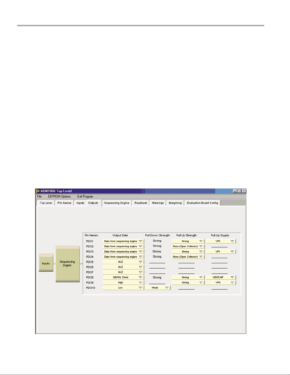
Figure 5 shows the GUI window for conguring the in
Table III details all of the registers used to congure the
outputs to perform the functions described above.
puts.
Figure 5. ADM106x Outputs Window
–14–
REV. 0
Page 15

AN-698
Table III.
Output Reg. Reg. Name Bits Bit Name R/W Description
PDO1 07H PDO1CFG 7 Cannot be used.
6:4 CFG6–CFG4 R/W
inter
CFG6 CFG5 CFG4 PDO Status
0 0 0 Disabled with weak pull-down
0 0 1 Enabled, follows the logic driven by the SE
0 1 0 Enables SMBus data, drive low
0 1 1 Enables SMBus data, drive high
3:0 CFG3–CFG0 R/W Determines the format of the pull-up on the PDO.
CFG3 CFG2 CFG1 CFG0 PDO Pull-Up
0 0 0 X None
0 0 1 X 300 k pull-up to VCP
0 1 0 0 Weak open drain pull-up to VP1
0 1 0 1 Push-pull pull-up to VP1
0 1 1 0 Weak open drain pull-up to VP2
0 1 1 1 Push-pull pull-up to VP2
1 0 0 0 Weak open drain pull-up to VP3
1 0 0 1 Push-pull pull-up to VP3
1 0 1 0 Weak open drain pull-up to VP4
1 0 1 1 Push-pull pull-up to VP4
1 1 1 0 Weak open drain pull-up to V
1 1 1 1 Push-pull pull-up to V
Controls the logic source driving the PDO, i.e., the SE, the
nal clock, or the SMBus, directly.
DD
DD
REV. 0
–15–
Page 16

AN-698
–17–
AN-698
REV. 0
Table III. (continued)
Output Reg. Reg. Name Bits Bit Name R/W Description
PDO2 0FH PDO2CFG 7 Cannot be used.
6:4 CFG6–CFG4 R/W Controls the logic source driving the PDO, i.e., the SE, the internal
clock, or the SMBus, directly.
CFG6 CFG5 CFG4 PDO Status
0 0 0 Disabled with weak pull-down
0 0 1 Enabled, follows the logic driven by the SE
0 1 0 Enables SMBus data, drive low
0 1 1 Enables SMBus data, drive high
3:0 CFG3–CFG0 R/W Determines the format of the pull-up on the PDO.
CFG3 CFG2 CFG1 CFG0 PDO Pull-Up
0 0 0 X None
0 0 1 X 300 k pull-up to VCP
0 1 0 0 Weak open drain pull-up to VP1
0 1 0 1 Push-pull pull-up to VP1
0 1 1 0 Weak open drain pull-up to VP2
0 1 1 1 Push-pull pull-up to VP2
1 0 0 0 Weak open drain pull-up to VP3
1 0 0 1 Push-pull pull-up to VP3
1 0 1 0 Weak open drain pull-up to VP4
1 0 1 1 Push-pull pull-up to VP4
1 1 1 0 Weak open drain pull-up to V
1 1 1 1 Push-pull pull-up to V
DD
DD
–16–
REV. 0
Page 17

AN-698
Table III. (continued)
Output Reg. Reg. Name Bits Bit Name R/W Description
PDO3 17H PDO3CFG 7 Cannot be used.
6:4 CFG6–CFG4 R/W Controls the logic source driving the PDO, i.e., the SE, the internal
clock, or the SMBus, directly.
CFG6 CFG5 CFG4 PDO Status
0 0 0 Disabled with weak pull-down
0 0 1 Enabled, follows the logic driven by the SE
0 1 0 Enables SMBus data, drive low
0 1 1 Enables SMBus data, drive high
3:0 CFG3–CFG0 R/W Determines the format of the pull-up on the PDO.
CFG3 CFG2 CFG1 CFG0 PDO Pull-Up
0 0 0 X None
0 0 1 X 300 k pull-up to VCP
0 1 0 0 Weak open drain pull-up to VP1
0 1 0 1 Push-pull pull-up to VP1
0 1 1 0 Weak open drain pull-up to VP2
0 1 1 1 Push-pull pull-up to VP2
1 0 0 0 Weak open drain pull-up to VP3
1 0 0 1 Push-pull pull-up to VP3
1 0 1 0 Weak open drain pull-up to VP4
1 0 1 1 Push-pull pull-up to VP4
1 1 1 0 Weak open drain pull-up to V
1 1 1 1 Push-pull pull-up to V
DD
DD
REV. 0
–17–
Page 18

AN-698
–19–
AN-698
REV. 0
Table III. (continued)
Output Reg. Reg. Name Bits Bit Name R/W Description
PDO4 1FH PDO4CFG 7 Cannot be used.
6:4 CFG6–CFG4 R/W Controls the logic source driving the PDO, i.e., the SE, the internal
clock, or the SMBus, directly.
CFG6 CFG5 CFG4 PDO Status
0 0 0 Disabled with weak pull-down
0 0 1 Enabled, follows the logic driven by the SE
0 1 0 Enables SMBus data, drive low
0 1 1 Enables SMBus data, drive high
3:0 CFG3–CFG0 R/W Determines the format of the pull-up on the PDO
CFG3 CFG2 CFG1 CFG0 PDO Pull-Up
0 0 0 X none
0 0 1 X 300 k pull-up to VCP
0 1 0 0 Weak open drain pull-up to VP1
0 1 0 1 Push-pull pull-up to VP1
0 1 1 0 Weak open drain pull-up to VP2
0 1 1 1 Push-pull pull-up to VP2
1 0 0 0 Weak open drain pull-up to VP3
1 0 0 1 Push-pull pull-up to VP3
1 0 1 0 Weak open drain pull-up to VP4
1 0 1 1 Push-pull pull-up to VP4
1 1 1 0 Weak open drain pull-up to V
1 1 1 1 Push-pull pull-up to V
DD
DD
–18–
REV. 0
Page 19

AN-698
Table III. (continued)
Output Reg. Reg. Name Bits Bit Name R/W Description
PDO5 27H PDO5CFG 7 Cannot be used.
6:4 CFG6–CFG4 R/W Controls the logic source driving the PDO, i.e., the SE, the internal
clock, or the SMBus, directly.
CFG6 CFG5 CFG4 PDO Status
0 0 0 Disabled with weak pull-down
0 0 1 Enabled, follows the logic driven by the SE
0 1 0 Enables SMBus data, drive low
0 1 1 Enables SMBus data, drive high
3:0 CFG3–CFG0 R/W Determines the format of the pull-up on the PDO.
CFG3 CFG2 CFG1 CFG0 PDO Pull-Up
0 0 0 X None
0 0 1 X 300 k pull-up to VCP
0 1 0 0 Weak open drain pull-up to VP1
0 1 0 1 Push-pull pull-up to VP1
0 1 1 0 Weak open drain pull-up to VP2
0 1 1 1 Push-pull pull-up to VP2
1 0 0 0 Weak open drain pull-up to VP3
1 0 0 1 Push-pull pull-up to VP3
1 0 1 0 Weak open drain pull-up to VP4
1 0 1 1 Push-pull pull-up to VP4
1 1 1 0 Weak open drain pull-up to V
1 1 1 1 Push-pull pull-up to V
DD
DD
REV. 0
–19–
Page 20

AN-698
–21–
AN-698
REV. 0
Table III. (continued)
Output Reg. Reg. Name Bits Bit Name R/W Description
PDO6 2FH PDO6CFG 7 Cannot be used.
6:4 CFG6–CFG4 R/W Controls the logic source driving the PDO, i.e., the SE, the internal
clock, or the SMBus, directly.
CFG6 CFG5 CFG4 PDO Status
0 0 0 Disabled with weak pull-down
0 0 1 Enabled, follows the logic driven by the SE
0 1 0 Enables SMBus data, drive low
0 1 1 Enables SMBus data, drive high
3:0 CFG3–CFG0 R/W Determines the format of the pull-up on the PDO.
CFG3 CFG2 CFG1 CFG0 PDO Pull-Up
0 0 0 X None
0 0 1 X 300 k pull-up to VCP
0 1 0 0 Weak open drain pull-up to VP1
0 1 0 1 Push-pull pull-up to VP1
0 1 1 0 Weak open drain pull-up to VP2
0 1 1 1 Push-pull pull-up to VP2
1 0 0 0 Weak open drain pull-up to VP3
1 0 0 1 Push-pull pull-up to VP3
1 0 1 0 Weak open drain pull-up to VP4
1 0 1 1 Push-pull pull-up to VP4
1 1 1 0 Weak open drain pull-up to V
1 1 1 1 Push-pull pull-up to V
DD
DD
–20–
REV. 0
Page 21

AN-698
Table III. (continued)
Output Reg. Reg. Name Bits Bit Name R/W Description
PDO7 37H PDO7CFG 7 Cannot be used.
6:4 CFG6–CFG4 R/W Controls the logic source driving the PDO, i.e., the SE, the internal
clock, or the SMBus, directly.
CFG6 CFG5 CFG4 PDO Status
0 0 0 Disabled, with weak pull-down
0 0 1 Enabled, follows the logic driven by the SE
0 1 0 Enables SMBus data, drive low
0 1 1 Enables SMBus data, drive high
3:0 CFG3–CFG0 R/W Determines the format of the pull-up on the PDO.
CFG3 CFG2 CFG1 CFG0 PDO Pull-Up
0 0 0 X None
0 0 1 X 300 k pull-up to VCP
0 1 0 0 Weak open drain pull-up to VP1
0 1 0 1 Push-pull pull-up to VP1
0 1 1 0 Weak open drain pull-up to VP2
0 1 1 1 Push-pull pull-up to VP2
1 0 0 0 Weak open drain pull-up to VP3
1 0 0 1 Push-pull pull-up to VP3
1 0 1 0 Weak open drain pull-up to VP4
1 0 1 1 Push-pull pull-up to VP4
1 1 1 0 Weak open drain pull-up to V
1 1 1 1 Push-pull pull-up to VDD
DD
REV. 0
–21–
Page 22

AN-698
–23–
AN-698
REV. 0
Table III. (continued)
Output Reg. Reg. Name Bits Bit Name R/W Description
PDO8 3FH PDO8CFG 7 Cannot be used.
6:4 CFG6–CFG4 R/W Controls the logic source driving the PDO, i.e., the SE, the internal
clock, or the SMBus, directly.
CFG6 CFG5 CFG4 PDO Status
0 0 0 Disabled with weak pull-down
0 0 1 Enabled, follows the logic driven by the SE
0 1 0 Enables SMBus data, drive low
0 1 1 Enables SMBus data, drive high
3:0 CFG3–CFG0 R/W Determines the format of the pull-up on the PDO.
CFG3 CFG2 CFG1 CFG0 PDO Pull-Up
0 0 0 X None
0 0 1 X 300 k pull-up to VCP
0 1 0 0 Weak open drain pull-up to VP1
0 1 0 1 Push-pull pull-up to VP1
0 1 1 0 Weak open drain pull-up to VP2
0 1 1 1 Push-pull pull-up to VP2
1 0 0 0 Weak open drain pull-up to VP3
1 0 0 1 Push-pull pull-up to VP3
1 0 1 0 Weak open drain pull-up to VP4
1 0 1 1 Push-pull pull-up to VP4
1 1 1 0 Weak open drain pull-up to V
1 1 1 1 Push-pull pull-up to V
DD
DD
–22–
REV. 0
Page 23

AN-698
Table III. (continued)
Output Reg. Reg. Name Bits Bit Name R/W Description
PDO9 47H PDO9CFG 7 Cannot be used.
6:4 CFG6–CFG4 R/W Controls the logic source driving the PDO, i.e., the SE, the internal
clock, or the SMBus, directly.
CFG6 CFG5 CFG4 PDO Status
0 0 0 Disabled, with weak pull-down
0 0 1 Enabled, follows the logic driven by the SE
0 1 0 Enables SMBus data, drive low
0 1 1 Enables SMBus data, drive high
3:0 CFG3–CFG0 R/W Determines the format of the pull-up on the PDO.
CFG3 CFG2 CFG1 CFG0 PDO Pull-Up
0 0 0 X None
0 0 1 X 300 k pull-up to VCP
0 1 0 0 Weak open drain pull-up to VP1
0 1 0 1 Push-pull pull-up to VP1
0 1 1 0 Weak open drain pull-up to VP2
0 1 1 1 Push-pull pull-up to VP2
1 0 0 0 Weak open drain pull-up to VP3
1 0 0 1 Push-pull pull-up to VP3
1 0 1 0 Weak open drain pull-up to VP4
1 0 1 1 Push-pull pull-up to VP4
1 1 1 0 Weak open drain pull-up to V
1 1 1 1 Push-pull pull-up to V
DD
DD
REV. 0
–23–
Page 24

AN-698
–25–
AN-698
REV. 0
Table III. (continued)
Output Reg. Reg. Name Bits Bit Name R/W Description
PDO10 4FH PDO10CFG 7 Cannot be used.
6:4 CFG6–CFG4 R/W Controls the logic source driving the PDO, i.e., the SE, the internal
clock, or the SMBus, directly.
CFG6 CFG5 CFG4 PDO Status
0 0 0 Disabled with weak pull-down
0 0 1 Enabled, follows the logic driven by the SE
0 1 0 Enables SMBus data, drive low
0 1 1 Enables SMBus data, drive high
3:0 CFG3–CFG0 R/W Determines the format of the pull-up on the PDO.
CFG3 CFG2 CFG1 CFG0 PDO Pull-Up
0 0 0 X None
0 0 1 X 300 k pull-up to VCP
0 1 0 0 Weak open drain pull-up to VP1
0 1 0 1 Push-pull pull-up to VP1
0 1 1 0 Weak open drain pull-up to VP2
0 1 1 1 Push-pull pull-up to VP2
1 0 0 0 Weak open drain pull-up to VP3
1 0 0 1 Push-pull pull-up to VP3
1 0 1 0 Weak open drain pull-up to VP4
1 0 1 1
1 1 1 0
1 1 1 1
Push-pull pull-up
Weak open drain pull-up
Push-pull pull-up
to VP4
to V
DD
to V
DD
–24–
REV. 0
Page 25

AN-698
STATE
MONITOR
FA
ULT
END-OF-STEP
TIMEOUT
ADM1066 SEQUENCING ENGINE
The ADM1066 incorporates a sequencing engine (SE)
that provides the user with powerful and exible
of sequencing. The SE implements a state ma
control
chine control
of the PDO outputs, with state changes conditional on
input events. SE programs can enable complex control
of boards, such as power- up and power-down sequence
control, fault event handling, and interrupt generation on
warnings. A watchdog function to verify the continued
operation of a processor clock can be integrated into
the SE program. The SE can also be controlled via the
SMBus, giving software or rmware control of the board
sequencing.
Considering the function of the SE from an applications
viewpoint, it is most instructive to think of the SE as
providing a state for a state machine. This state has the
following attributes:
•
It is used to monitor signals indicating the status of
the 10 input pins, VP1–VP4, VH, and VX1–VX5.
•
It can be entered from any other state.
•
There are three exit routes which move the state
machine on to a next state.
1. End- of- step detection
2. Monitoring fault
3. Timeout
•
Delay timers for the end- of-step and timeout blocks
can be programmed independently and change with
each state change. The range of timeouts is from
0 ms to 400 ms.
•
The output condition of the 10 PDO pins is dened
and xed within a state.
•
The transition from one state to the next is made in
less than 20 µs. This is the time taken to download a
state denition from EEPROM to the SE.
Figure 6. State Cell
The ADM106x offers up to 63 such state denitions. Each
state is dened by a 64-bit word.
Figure 7 shows the GUI window for conguring the in
puts.
Table IV shows the detail of the 64 bits that dene a state.
Table VII details how to communicate with the SE.
REV. 0
Figure 7. ADM106x Sequencing Engine Window
–25–
Page 26

AN-698
–27–
AN-698
REV. 0
Table IV. Starting Address for Each State in SE
State Start Address
State 0 FA00
State 1 FA08
State 2 FA10
State 3 FA18
State 4 FA20
State 5 FA28
State 6 FA30
State 7 FA38
State 8 FA40
State 9 FA48
State 10 FA50
State 11 FA58
State 12 FA60
State 13 FA68
State 14 FA70
State 15 FA78
State 16 FA80
State 17 FA88
State 18 FA90
State 19 FA98
State 20 FAA0
State 21 FAA8
State 22 FAB0
State 23 FAB8
State 24 FAC0
State 25 FAC8
State 26 FAD0
State 27 FAD8
State 28 FAE0
State 29 FAE8
State 30 FAF0
State 31 FAF8
State Start Address
State 32 FB00
State 33 FB08
State 34 FB10
State 35 FB18
State 36 FB20
State 37 FB28
State 38 FB30
State 39 FB38
State 40 FB40
State 41 FB48
State 42 FB50
State 43 FB58
State 44 FB60
State 45 FB68
State 46 FB70
State 47 FB78
State 48 FB80
State 49 FB88
State 50 FB90
State 51 FB98
State 52 FBA0
State 53 FBA8
State 54 FBB0
State 55 FBB8
State 56 FBC0
State 57 FBC8
State 58 FBD0
State 59 FBD8
State 60 FBE0
State 61 FBE8
State 62 FBF0
State 63 FBF8
–26–
REV. 0
Page 27

AN-698
Table V. Bitmap for Denition of Each State in SE
Operation,
Bit or If 0… If 1… Notes
0 PDO1 Output Data
1 PDO2 Output Data
2 PDO3 Output Data
3 PDO4 Output Data
4 PDO5 Output Data
5 PDO6 Output Data
6 PDO7 Output Data
7 PDO8 Output Data
8 PDO9 Output Data
9 PDO10 Output Data
10 Monitor Fault if VP1 = 0 Monitor Fault if VP1 = 1 Monitoring of faults on VP1 must be unmasked for this
function to execute (next bit).
11 Mask VP1 Monitoring Unmask VP1 Monitoring Bit 11 = 1; turns on monitoring on VP1 channel.
12 Monitor Fault if VP2 = 0 Monitor Fault if VP2 = 1 Monitoring of faults on VP2 must be unmasked for this
function to execute (next bit).
13 Mask VP2 Monitoring Unmask VP2 Monitoring Bit 13 = 1; turns on monitoring on VP2 channel.
14 Monitor Fault if VP3 = 0 Monitor Fault if VP3 = 1 Monitoring of faults on VP3 must be unmasked for this
function to execute (next bit).
15 Mask VP3 Monitoring Unmask VP3 Monitoring Bit 15 = 1; turns on monitoring on VP3 channel.
16 Monitor Fault if VP4 = 0 Monitor Fault if VP4 = 1 Monitoring of faults on VP4 must be unmasked for this
function to execute (next bit).
17 Mask VP4 Monitoring Unmask VP4 Monitoring Bit 17 = 1; turns on monitoring on VP4 channel.
18 Monitor Fault if VH = 0 Monitor Fault if VH = 1 Monitoring of faults on VH must be unmasked for this
function to execute (next bit).
19 Mask VH Monitoring Unmask VH Monitoring Bit 19 = 1; turns on monitoring on VH channel.
20 Monitor Fault if VX1 = 0 Monitor Fault if VX1 = 1 Monitoring of faults on VX1 must be unmasked for this
function to execute (next bit).
21 Mask VX1 Monitoring Unmask VX1 Monitoring Bit 21 = 1; turns on monitoring on VX1 channel.
22 Monitor Fault if VX2 = 0 Monitor Fault if VX2 = 1 Monitoring of faults on VX2 must be unmasked for this
function to execute (next bit).
23 Mask VX2 Monitoring Unmask VX2 Monitoring Bit 23 = 1; turns on monitoring on VX2 channel.
24 Monitor Fault if VX3 = 0 Monitor Fault if VX3 = 1 Monitoring of faults on VX3 must be unmasked for this
function to execute (next bit).
25 Mask VX3 Monitoring Unmask VX3 Monitoring Bit 25 = 1; turns on monitoring on VX3 channel.
26 Monitor Fault if VX4 = 0 Monitor Fault if VX4 = 1 Monitoring of faults on VX4 must be unmasked for this
function to execute (next bit).
27 Mask VX4 Monitoring Unmask VX4 Monitoring Bit 27 = 1; turns on monitoring on VX5 channel.
28 Monitor Fault if VX5 = 0 Monitor Fault if VX5 = 1 Monitoring of faults on VX4 must be unmasked for this
function to execute (next bit).
29 Mask VX5 Monitoring Unmask VX5 Monitoring Bit 29 = 1; turns on monitoring on VX5 channel.
30 Mask WARNING Unmask WARNING Can only generate a monitor fault on WARNING = 1.
Monitoring Monitoring Is unmasked.
REV. 0
–27–
Page 28

AN-698
–29–
AN-698
REV. 0
Table V. Bitmap for Denition of Each State in SE (continued)
Operation,
Bit or If 0… If 1… Notes
31 TIMEOUT<0> Timeout length (see overleaf).
32 TIMEOUT<1>
33 TIMEOUT<2>
34 TIMEOUT<3>
35 SEQCOND<0> Sequence condition (see overleaf).
36 SEQCOND<1>
37 SEQCOND<2>
38 SEQCOND<3>
39 Sequence on Selected Sequence on Selected SEQSENSE
Input = High Input = Low
40 SEQDELAY<0> Sequence delay (see overleaf).
41 SEQDELAY<1>
42 SEQDELAY<2>
43 SEQDELAY<3>
44 MONADDR<0> MONADDR<5:0> is the state number to jump to if a monitor
function fault occurs.
45 MONADDR<1>
46 MONADDR<2>
47 MONADDR<3>
48 MONADDR<4>
49 MONADDR<5>
50 TIMADDR<0> TIMADDR<5:0> is the state number to jump to if a timeout
fault occurs.
51 TIMADDR<1>
52 TIMADDR<2>
53 TIMADDR<3>
54 TIMADDR<4>
55 TIMADDR<5>
56 SEQADDR<0> SEQADDR<5:0> is the state number to jump to if a sequence
fault occurs.
57 SEQADDR<1>
58 SEQADDR<2>
59 SEQADDR<3>
60 SEQADDR<4>
61 SEQADDR<5>
62 Round Robin Disable Round Robin Enable This is OR’d with RRCTRL.2.
63 Fault Latch Closed Fault Latch Open
–28–
REV. 0
Page 29

Table VI. Timeouts and Delays for Functions in SE
TIMEOUT<3:0> SEQDELAY<3:0>Delay (ms)
0 0
1 0.1
2 0.2
3 0.4
4 0.7
5 1
6 2
7 4
8 7
9 10
10 20
11 40
12 70
13 100
14 200
15 400
AN-698
SEQCOND<3:0> Sequence On Signal From
0 “Never” Never sequence; set SEQSENSE = 0 always to ensure no sequence (bit 39).
1 VP1
2 VP2
3 VP3
4 VP4
5 VH
6 VX1
7 VX2
8 VX3
9 VX4
10 VX5
11 WARNING
12 SWFLOW; Unconditional GOTO; always set SEQSENSE = 0 to ensure proper operation.
Table VII. Communicating with the SE
Reg. Reg. Name Bits Bit Name R/W Description
93H SECTRL 7:3 Cannot be used.
E9 SEADDR 7:6
5:0 ADDR R SE current state used in conjunction with 93H:0.
2 SWCONTINUE W Allows software control of SE state changes. Can force an unconditional
jump to the next state. The bit can be set as the condition for an end-of-step
change. This enables the user to clear external interrupts by moving forward
a state. The bit self clears to 0 after the state change has occurred.
1 SWSTEP R/W Step the SE forward to the next state. Use in conjunction with the HALT bit to
step through a sequence. Can be used as a tool for debugging sequences.
0 HALT R/W Halt the SE. State changes will not happen. Must be set to allow read, erase,
or write access to the SE EEPROM.
REV. 0
–29–
Page 30

AN-698
–31–
AN-698
REV. 0
ADM106x ADC
The ADM1062, ADM1063, ADM1064, and ADM1066 all
feature an on - chip 12-bit ADC. The ADC has a 12 (13 on
the ADM1063) channel analog mux on the front end. Any
or all of these inputs can be selected to be read by the
ADC. Thus the ADC can be set up to continuously read
the
selected channels. The circuit controlling this operation is called the round robin. The user selects which
channels they wish to operate on and the ADC performs
a conversion on each in turn. Averaging can be turned
on, setting the round robin to take 16 conversions on
each channel; other wise, a single conversion is made
on each channel. At the end of this cycle, the results
are all written to the output registers and, at the same
time, compared with preset thresholds provided on the
ADM106x which can be programmed to a maximum or
minimum allowable threshold. Only one register is pro vided for each input channel so a UV or OV threshold,
but not both, can be set for a given channel. Exceeding
the threshold generates a warning that can be read back
from the status registers or input into the SE via an OR
gate. The round robin can be enabled via an SMBus
write, or can be programmed to turn on at any particular point in the SE program; for instance, it can be set to
start once a power- up sequence is complete and all supplies are known to be within expected fault limits.
Figure 8 shows the GUI window for conguring the ADC.
Table VIII shows the detail of the registers required to set
up the ADC and its inputs.
Figure 8. ADM106x ADC Readback Window
–30–
REV. 0
Page 31

AN-698
Table VIII. ADC Readback Conguration Registers
Input Reg. Reg. Name Bits Bit Name R/W Description
Limit Registers—an ADC reading above or below this limit generates a warning.
VP1 70H ADCVP1LIM 7:0 LIM7–LIM0 R/W Limit register for ADC conversion on VP1 input
VP2 71H ADCVP2LIM 7:0 LIM7–LIM0 R/W Limit register for ADC conversion on VP2 input
VP3 72H ADCVP3LIM 7:0 LIM7–LIM0 R/W Limit register for ADC conversion on VP3 input
VP4 73H ADCVP4LIM 7:0 LIM7–LIM0 R/W Limit register for ADC conversion on VP4 input
VH 74H ADCVHLIM 7:0 LIM7–LIM0 R/W Limit register for ADC conversion on VH input
VX1 75H ADCVX1LIM 7:0 LIM7–LIM0 R/W Limit register for ADC conversion on VX1 input
VX2 76H ADCVX2LIM 7:0 LIM7–LIM0 R/W Limit register for ADC conversion on VX2 input
VX3 77H ADCVX3LIM 7:0 LIM7–LIM0 R/W Limit register for ADC conversion on VX3 input
VX4 78H ADCVX4LIM 7:0 LIM7–LIM0 R/W Limit register for ADC conversion on VX4 input
VX5 79H ADCVX5LIM 7:0 LIM7–LIM0 R/W Limit register for ADC conversion on VX5 input
IN TS 7AH ADCITLIM 7:0 LIM7–LIM0 R/W Limit register for ADC conversion on internal temp sensor
(ADM1062, ADM1063 only)
AUX1 7AH ADCAUX1LIM 7:0 LIM7–LIM0 R/W Limit register for ADC conversion on Aux 1 channel
(ADM1064, ADM1066 only)
EXTS1 7BH ADCXT1LIM 7:0 LIM7–LIM0 R/W Limit register for ADC conversion on external temp sensor 1
(ADM1062, ADM1063 only)
AUX2 7BH ADCAUX2LIM 7:0 LIM7–LIM0 R/W Limit register for ADC conversion on external temp sensor 1
(ADM1064, ADM1066 only)
EXTS2 7CH ADCXT2LIM 7:0 LIM7–LIM0 R/W Limit register for ADC conversion on external temp sensor 2
(ADM1063 only)
Sense Registers—determines when a warning is generated.
VX3 7DH LSENSE1 7 SENS7 R/W Limit sense for VX3 (0 = ADC > LIMIT gives warning, i.e., OVERVOLTAGE,
1 = ADC < LIMIT gives a warning, i.e., UNDERVOLTAGE)
VX2 6 SENS6 R/W Limit sense for VX2 (0 = ADC > LIMIT gives warning, i.e., OVERVOLTAGE,
1 = ADC < LIMIT gives a warning, i.e., UNDERVOLTAGE)
VX1 5 SENS5 R/W Limit sense for VX1 (0 = ADC > LIMIT gives warning, i.e., OVERVOLTAGE,
1 = ADC < LIMIT gives a warning, i.e., UNDERVOLTAGE)
VH 4 SENS4 R/W Limit sense for VH (0 = ADC > LIMIT gives warning, i.e., OVERVOLTAGE,
1 = ADC < LIMIT gives a warning, i.e., UNDERVOLTAGE)
VP4 3 SENS3 R/W Limit sense for VP4 (0 = ADC > LIMIT gives warning, i.e., OVERVOLTAGE,
1 = ADC < LIMIT gives a warning, i.e., UNDERVOLTAGE)
VP3 2 SENS2 R/W Limit sense for VP3 (0 = ADC > LIMIT gives warning, i.e., OVERVOLTAGE,
1 = ADC < LIMIT gives a warning, i.e., UNDERVOLTAGE)
VP2 1 SENS1 R/W Limit sense for VP2 (0 = ADC > LIMIT gives warning, i.e., OVERVOLTAGE,
1 = ADC < LIMIT gives a warning, i.e., UNDERVOLTAGE)
VP1 0 SENS0 R/W Limit sense for VP1 (0 = ADC > LIMIT gives warning, i.e., OVERVOLTAGE,
1= ADC < LIMIT gives a warning, i.e., UNDERVOLTAGE)
REV. 0
–31–
Page 32

AN-698
–33–
AN-698
REV. 0
REV. 0
Table VIII. ADC Readback Conguration Registers
Input Reg. Reg. Name Bits Bit Name R/W Description
7EH LSENSE2 7 SENS7 Cannot be used.
6 SENS6 Cannot be used.
5 SENS5 Cannot be used.
EXTS2 4 SENS4 R/W
AUX2 3 SENS3 R/W Limit sense for AUX2 (ADM1064, ADM1066 only) (0 = ADC > LIMIT gives
EXTS1 3 SENS3 R/W Limit sense for External Temp Sensor 1 (ADM1062, ADM1063 only)
AUX1 2 SENS2 R/W Limit sense for AUX1 (ADM1064, ADM1066 only) (0 = ADC > LIMIT gives
INTS 2 SENS2 R/W Limit sense for Internal Temp Sensor (ADM1062, ADM1063 only)
VX5 1 SENS1 R/W Limit sense for VX5 (0 = ADC > LIMIT gives warning, i.e., OVERVOLTAGE,
VX4 0 SENS0 R/W Limit sense for VX4 (0 = ADC > LIMIT gives warning, i.e., OVERVOLTAGE,
Round Robin Select Registers—determine which inputs are actually read by the ADC as it cycles.
VX3 80H RRSEL1 7 VX3CHAN R/W 0 => VX3 is included in RR. 1 => VX3 is excluded from RR.
VX2 6 VX2CHAN R/W 0 => VX2 is included in RR. 1 => VX2 is excluded from RR.
VX1 5 VX1CHAN R/W 0 => VX1 is included in RR. 1 => VX1 is excluded from RR.
VH 4 VHCHAN R/W 0 => VH is included in RR. 1 => VH is excluded from RR.
VP4 3 VP4CHAN R/W 0 => VP4 is included in RR. 1 => VP4 is excluded from RR.
VP3 2 VP3CHAN R/W 0 => VP3 is included in RR. 1 => VP3 is excluded from RR.
VP2 1 VP2CHAN R/W 0 => VP2 is included in RR. 1 => VP2 is excluded from RR.
VP1 0 VP1CHAN R/W 0 => VP1 is included in RR. 1 => VP1 is excluded from RR.
Limit sense for External Temp Sensor 2 (ADM1063 only) (0 = ADC > LIMIT
gives warning, i.e., OVERVOLTAGE, 1 = ADC < LIMIT gives a warning,
i.e., UNDERVOLTAGE)
warning, i.e., OVERVOLTAGE, 1 = ADC < LIMIT gives a warning, i.e.,
UNDERVOLTAGE)
ADC > LIMIT gives warning, i.e., OVERVOLTAGE, 1 = ADC < LIMIT gives
a
warning,
warning, i.e., OVERVOLTAGE, 1 = ADC < LIMIT gives a warning, i.e.,
UNDERVOLTAGE)
ADC > LIMIT gives warning, i.e., OVERVOLTAGE, 1 = ADC < LIMIT gives
a
warning, i.e., UNDERVOLTAGE)
1 = ADC < LIMIT gives a warning, i.e., UNDERVOLTAGE)
1 = ADC < LIMIT gives a warning, i.e., UNDERVOLTAGE)
i.e.,
UNDERVOLTAGE)
(continued)
(0 =
(0 =
–32–
Page 33

AN-698
Table VIII. ADC Readback Conguration Registers
Input Reg. Reg. Name Bits Bit Name R/W Description
6 Cannot be used.
5 Cannot be used.
EXTS2 4 EXTCH2 R/W 0 => External Temp Sensor 2 is included in RR. 1=>External Temp
Sensor 2 is excluded from RR (ADM1063 only).
AUX2 3 AUX2CHAN R/W
is excluded from RR (ADM1064, ADM1066 only).
EXTS1 3 EXTCH1 R/W 0 => External Temp Sensor 1 is included in RR. 1=> External Temp
Sensor 1 is excluded from RR (ADM1062, ADM1063 only).
AUX1 2 AUX1CHAN R/W
is excluded from RR (ADM1064, ADM1066 only).
INTS 2 INTCH1 R/W 0 => Internal Temp Sensor 1 is included in RR. 1=> Internal Temp
Sensor 1 is excluded from RR (ADM1062, ADM1063 only).
VX5 1 VX5CHAN R/W 0 => VX5 is included in RR. 1=> VX5 is excluded from RR.
VX4 0 VX4CHAN R/W 0 => VX4 is included in RR. 1=> VX4 is excluded from RR.
Round Robin Control Register—activates ADC read. Determines if averaging is used and if continuous read.
82H RRCTRL 7:5 Cannot be used.
4 CLEARLIM R/W Write this bit high to clear limit warnings. This bit then self clears.
3 STOPWRITE R/W Inhibits the RR from writing the results to the output registers.
2 AVERAGE R/W Turn on 16 averaging.
1 ENABLE R/W Turn on the RR for continuous operation.
0 GO R/W Start the RR.
Temp Sensor Conguration Register
83H TSCTRL 7:3 Cannot be used.
2 LOWDN2 R/W Turn off VBE biasing for D2N (ADM1063 only).
1 LOWDN1 R/W Turn off VBE biasing for D1N.
0 DIODE_CK R/W
81H RRSEL2 7 Cannot be used.
0 => Auxilliary Channel 2 is included in RR. 1=> Auxilliary Channel
0 => Auxilliary Channel 1 is included in RR. 1=> Auxilliary Channel
Set this bit to perform a diode check. If set, this causes the ADC result
for the two external channels to limit at full-scale positive if a di
is present. Used for board checking.
(continued)
ode
2
1
REV. 0
–33–
Page 34

AN-698
–35–
AN-698
REV. 0
Table VIII. ADC Readback Conguration Registers
Input Reg. Reg. Name Bits Bit Name R/W Description
ADC Value Registers
VP1 A0H ADCHVP1 7:4 Not used if 82H:2 (Average) = 0.
3:0 OUT3–OUT0 R/W 4 MSBs of 12-bit result of ADC conversions on VP1 when 82H:2
(Average) = 0.
7:0 OUT7–OUT0 R/W 8 MSBs of 16-bit result of ADC conversions on VP1 when 82H:2
(Average) = 1.
A1H ADCLVP1 7:0 OUT7–OUT0 R/W 8 LSBs of 12- or 16-bit result of the ADC conversions on VP1 input.
VP2 A2H ADCHVP2 7:4 Not used if 82H:2 (Average) = 0.
3:0 OUT3–OUT0 R/W 4 MSBs of 12-bit result of ADC conversions on VP2 when 82H:2
(Average) = 0.
7:0 OUT7–OUT0 R/W 8 MSBs of 16-bit result of ADC conversions on VP2 when 82H:2
(Average) = 1.
A3H ADCLVP2 7:0 OUT7–OUT0 R/W 8 LSBs of 12- or 16-bit result of the ADC conversions on VP2 input.
VP3 A4H ADCHVP3 7:4 Not used if 82H:2 (Average) = 0.
3:0 OUT3–OUT0 R/W 4 MSBs of 12-bit result of ADC conversions on VP3 when 82H:2
(Average) = 0.
7:0 OUT7–OUT0 R/W 8 MSBs of 16-bit result of ADC conversions on VP3 when 82H:2
(Average) = 1.
A5H ADCLVP3 7:0 OUT7–OUT0 R/W 8 LSBs of 12- or 16-bit result of the ADC conversions on VP3 input.
VP4 A6H ADCHVP4 7:4 Not used if 82H:2 (Average) = 0.
3:0 OUT3–OUT0 R/W 4 MSBs of 12-bit result of ADC conversions on VP4 when 82H:2
(Average) = 0.
7:0 OUT7–OUT0 R/W 8 MSBs of 16-bit result of ADC conversions on VP4 when 82H:2
(Average) = 1.
A7H ADCLVP4 7:0 OUT7–OUT0 R/W 8 LSBs of 12- or 16-bit result of the ADC conversions on VP4 input.
VH A8H ADCHVH 7:4 Not used if 82H:2 (Average) = 0.
3:0 OUT3–OUT0 R/W 4 MSBs of 12-bit result of ADC conversions on VH when 82H:2
(Average) = 0.
7:0 OUT7–OUT0 R/W 8 MSBs of 16-bit result of ADC conversions on VH when 82H:2
(Average) = 1.
A9H ADCLVH 7:0 OUT7–OUT0 R/W 8 LSBs of 12- or 16-bit result of the ADC conversions on VH input.
VX1 AAH ADCHVX1 7:4 Not used if 82H:2 (Average) = 0.
3:0 OUT3–OUT0 R/W 4 MSBs of 12-bit result of ADC conversions on VX1 when 82H:2
(Average) = 0.
7:0 OUT7–OUT0 R/W 8 MSBs of 16-bit result of ADC conversions on VX1 when 82H:2
(Average) = 1.
ABH ADCLVX1 7:0 OUT7–OUT0 R/W 8 LSBs of 12- or 16-bit result of the ADC conversions on VX1 input.
VX2 ACH ADCHVX2 7:4 Not used if 82H:2 (Average) = 0.
3:0 OUT3–OUT0 R/W 4 MSBs of 12-bit result of ADC conversions on VX2 when 82H:2
(Average) = 0.
7:0 OUT7–OUT0 R/W 8 MSBs of 16-bit result of ADC conversions on VX2 when 82H:2
(Average) = 1.
ADH ADCLVX2 7:0 OUT7–OUT0 R/W 8 LSBs of 12- or 16-bit result of the ADC conversions on VX2 input.
(continued)
–34–
REV. 0
Page 35

AN-698
Table VIII. ADC Readback Conguration Registers
Input Reg. Reg. Name Bits Bit Name R/W Description
VX3 AEH ADCHVX3 7:4 Not used if 82H:2 (Average) = 0.
3:0 OUT3–OUT0 R/W 4 MSBs of 12-bit result of ADC conversions on VX3 when 82H:2
(Average) = 0.
7:0 OUT7–OUT0 R/W 8 MSBs of 16-bit result of ADC conversions on VX3 when 82H:2
(Average) = 1.
AFH ADCLVX3 7:0 OUT7–OUT0 R/W 8 LSBs of 12- or 16-bit result of the ADC conversions on VX3 input.
VX4 B0H ADCHVX4 7:4 Not used if 82H:2 (Average) = 0.
3:0 OUT3–OUT0 R/W 4 MSBs of 12-bit result of ADC conversions on VX4 when 82H:2
(Average) = 0.
7:0 OUT7–OUT0 R/W 8 MSBs of 16-bit result of ADC conversions on VX4 when 82H:2
(Average) = 1.
B1H ADCLVX4 7:0 OUT7–OUT0 R/W 8 LSBs of 12- or 16-bit result of the ADC conversions on VX4 input.
VX5 B2H ADCHVX5 7:4 Not used if 82H:2 (Average) = 0.
3:0 OUT3–OUT0 R/W 4 MSBs of 12-bit result of ADC conversions on VX5 when 82H:2
(Average) = 0.
7:0 OUT7–OUT0 R/W 8 MSBs of 16-bit result of ADC conversions on VX5 when 82H:2
(Average) = 1.
B3H ADCLVX5 7:0 OUT7–OUT0 R/W 8 LSBs of 12- or 16-bit result of the ADC conversions on VX5 input.
INTS B4H ADCHITS 7:4 Not used if 82H:2 (Average) = 0.
3:0 OUT3–OUT0 R/W 4 MSBs of 12-bit result of Internal Temp Sensor conversion
(ADM1062, ADM1063 only).
7:0 OUT7–OUT0 R/W 8 MSBs of 16-bit result of Internal Temp Sensor conversion
(ADM1062, ADM1063 only).
B5H ADCLITS 7:0 OUT7–OUT0 R/W
AUX1 B4H ADCHAUX1 7:4 Not used if 82H:2 (Average) = 0.
3:0 OUT3–OUT0 R/W 4 MSBs of 12-bit result of AUX1 conversion (ADM1064,
7:0 OUT7–OUT0 R/W 8 MSBs of 16-bit result of AUX1 conversion (ADM1064,
B5H ADCLAUX1 7:0 OUT7–OUT0 R/W Low Byte of AUX1 conversion (ADM1064, ADM1066 only).
EXTS1 B6H ADCHXTS1 7:4 Not used if 82H:2 (Average) = 0.
3:0 OUT3–OUT0 R/W 4 MSBs of 12-bit result of External Temp Sensor 1 conversion
7:0 OUT7–OUT0 R/W 8 MSBs of 16-bit result of External Temp Sensor 1 conversion
B7H ADCLXTS1 7:0 OUT7–OUT0 R/W Low Byte of External Temp Sensor 1 conversion (ADM1062,
AUX2 B6H ADCHAUX2 7:4 Not used if 82H:2 (Average) = 0.
3:0 OUT3–OUT0 R/W 4 MSBs of 12-bit result of AUX2 conversion (ADM1064,
7:0 OUT7–OUT0 R/W 8 MSBs of 16-bit result of AUX2 conversion (ADM1064,
Low Byte of Internal Temp Sensor conversion (ADM1062,
ADM1063
ADM1066 only).
ADM1066 only).
(ADM1062, ADM1063 only).
(ADM1062, ADM1063 only).
ADM1063 only).
ADM1066 only).
ADM1066 only).
only).
(continued)
B7H ADCLAUX2 7:0 OUT7–OUT0 R/W Low byte of AUX2 conversion (ADM1064, ADM1066 only).
REV. 0
–35–
Page 36

AN-698
–37–
AN-698
DACoutput DACn 0x7F V
OFF
=
( )
× +– 255 0.6015
DAC Code
DACn, DNLIMn DACn DPLIMn
DNLIMn, DACn DPLIMn
DPLIMn, DACn DPLIMn
=
≤ ≤
<
>
REV. 0
Table VIII. ADC Readback Conguration Registers
Input Reg. Reg. Name Bits Bit Name R/W Description
EXTS2 B8H ADCHXTS2 7:4 Not used if 82H:2 (Average) = 0.
3:0 OUT3–OUT0 R/W 4 MSBs of 12-bit result of External Temp Sensor 2 conversion
(ADM1063 only).
7:0 OUT7–OUT0 R/W 8 MSBs of 16-bit result of External Temp Sensor 2 conversion
(ADM1063 only).
B9H ADCLXTS2 7:0 OUT7–OUT0 R/W Low byte of External Temp Sensor 2 conversion (ADM1063 only).
ADM106x DACs
The ADM1062, ADM1066, and ADM1067 all feature six
voltage output DACs. These DACs are primarily used to
adjust the output voltage of a dc-dc converter by altering
the current at its feedback node. These DACs, therefore,
provide an open-loop margining system. The ADC on the
ADM1062 and ADM1066 closes this loop. For more information on margining, refer to the relevant data sheet.
When the DACn output buffer is turned on it has very
little effect on the dc-dc output. The DAC output buffer has been designed to power-up without glitching. It
does this by rst powering up the buffer to follow the pin
voltage and does not drive out on to the pin at this time.
Once the output buffer is properly enabled, the buf fer
input is switched over to the DAC and the output stage of
the buffer is turned on; output glitching is negligible.
Four DAC ranges are offered and these are placed with
midcode (code 0x7F) at 0.6 V, 0.8 V, 1.0 V, and 1.25 V.
These voltages are placed to correspond to the most
common feedback voltages. Centering the DAC outputs
in this way provides the best use of the DAC resolution,
i.e., for most supplies it will be possible to place the
DAC midcode at the point where the dc - dc output is not
modied, thus giving a full half each of the DAC range
to margin up and down. The DAC output voltage is set
by the code written to the DACn register. The voltage
is linear with the unsigned binary number in this reg ister. The code 0x7F is placed at the midcode voltage
as described above. The output voltage is given by the
following equation:
Limit registers (called DPLIMn and DNLIMn) on the
de
vice offer the user some protection from rmware
bugs which could cause catastrophic board problems by
forcing supplies beyond their allowable output ranges.
Essentially the DAC code written into the DACn register
is clipped so that the code used to set the DAC voltage
is actually given by
The DAC output buf fer is three -stated if DNLIMn >
DPLIMn. It is possible for the user to make it very difcult for the DAC output buffers to be turned on at all
in normal system operation by programming the limit
registers in this way (these are among the registers
downloaded from EEPROM at start- up).
Figure 9 shows the GUI window for conguring the DACs.
Table VIII shows the detail of the registers required to set
up the DACs.
(continued)
where V
above.
is one of the four offset voltages described
OFF
–36–
REV. 0
Page 37

AN-698
Figure 9. ADM106x DAC Window
Table IX. DAC Conguration Registers
Output Reg. Reg. Name Bits Bit Name R/W Description
DAC1 50H DACCTRL1 7:3 Cannot be used.
2 ENDAC R/W Enable DAC1
1:0 OFFSEL1-0 R/W Selects the center voltage (midcode) output of DAC1
OFFSEL1 OFFSEL0 (midcode) Output Voltage
0 0 1.25 V
0 1 1.0 V
1 0 0.8 V
1 1 0.6 V
58H DAC1 7:0 DAC7-0 R/W 8-bit DAC code (0x7f Is midcode)
60H DPLIM1 7:0 LIM7-0 R/W 8-bit DAC positive limit code. If DAC1 is set to a
higher code the DAC code limits to the contents
of this register.
68H DNLIM1 7:0 LIM7-0 R/W 8-bit DAC negative limit code. If DAC1 is set to a
lower code the DAC code limits to the contents of
this register.
Note: If DNLIM1 is set to be greater than DPLIM1
then the DAC output is always disabled (this is a
safety feature).
REV. 0
–37–
Page 38

AN-698
–39–
AN-698
REV. 0
Table IX. DAC Conguration Registers (continued)
Output Reg. Reg. Name Bits Bit Name R/W Description
DAC2 51H DACCTRL2 7:3 Cannot be used.
2 ENDAC R/W Enable DAC2
1:0 OFFSEL1-0 R/W Selects the center voltage (midcode) output of DAC2
OFFSEL1 OFFSEL0 (midcode) Output Voltage
0 0 1.25 V
0 1 1.0 V
1 0 0.8 V
1 1 0.6 V
59H DAC2 7:0 DAC7-0 R/W 8-bit DAC code (0x7f Is midcode)
61H DPLIM2 7:0 LIM7-0 R/W 8-bit DAC positive limit code. If DAC2 is set to a
higher code, the DAC code limits to the contents of
this register.
69H DNLIM2 7:0 LIM7-0 R/W 8-bit DAC negative limit code. If DAC2 is set to a
lower code, the DAC code limits to the contents of
this register.
Note: If DNLIM2 is set to be greater than DPLIM2,
then the DAC output is always disabled (this is a
safety feature).
–38–
REV. 0
Page 39

AN-698
Table IX. DAC Conguration Registers (continued)
Output Reg. Reg. Name Bits Bit Name R/W Description
DAC3 52H DACCTRL3 7:3 Cannot be used.
2 ENDAC R/W Enable DAC3
1:0 OFFSEL1-0 R/W Selects the center voltage (midcode) output of DAC3
OFFSEL1 OFFSEL0 (midcode) Output Voltage
0 0 1.25 V
0 1 1.0 V
1 0 0.8 V
1 1 0.6 V
5AH DAC3 7:0 DAC7-0 R/W 8-bit DAC code (0x7f Is midcode)
62H DPLIM3 7:0 LIM7-0 R/W 8-bit DAC positive limit code. If DAC3 is set to a
code higher than this, the DAC code limits to the
contents of this register.
6AH DNLIM3 7:0 LIM7-0 R/W 8-bit DAC negative limit code. If DAC3 is set to a
code lower than this, the DAC code limits to the
contents of this register.
Note: If DNLIM3 is set to be greater than DPLIM3,
then the DAC output is always disabled (this is a
safety feature).
REV. 0
–39–
Page 40

AN-698
–41–
AN-698
REV. 0
Table IX. DAC Conguration Registers (continued)
Output Reg. Reg. Name Bits Bit Name R/W Description
DAC4 53H DACCTRL4 7:3 Cannot be used.
2 ENDAC R/W Enable DAC4
1:0 OFFSEL1-0 R/W Selects the center voltage (midcode) output of DAC4
OFFSEL1 OFFSEL0 (midcode) Output Voltage
0 0 1.25 V
0 1 1.0 V
1 0 0.8 V
1 1 0.6 V
5BH DAC4 7:0 DAC7-0 R/W 8-bit DAC code (0x7f Is midcode)
63H DPLIM4 7:0 LIM7-0 R/W 8-bit DAC positive limit code. If DAC4 is set to a
higher code, the DAC code limits to the contents of
this register.
6BH DNLIM4 7:0 LIM7-0 R/W 8-bit DAC negative limit code. If DAC4 is set to a
lower code, the DAC code limits to the contents of
this register.
Note: If DNLIM4 is set to be greater than DPLIM4,
then the DAC output is always disabled (this is a
safety feature).
–40–
REV. 0
Page 41

AN-698
Table IX. DAC Conguration Registers (continued)
Output Reg. Reg. Name Bits Bit Name R/W Description
DAC5 54H DACCTRL5 7:3 Cannot be used.
2 ENDAC R/W Enable DAC5
1:0 OFFSEL1-0 R/W Selects the center voltage (midcode) output of DAC5
OFFSEL1 OFFSEL0 (midcode) Output Voltage
0 0 1.25 V
0 1 1.0 V
1 0 0.8 V
1 1 0.6 V
5CH DAC5 7:0 DAC7-0 R/W 8-bit DAC code (0x7f Is midcode)
64H DPLIM5 7:0 LIM7-0 R/W 8-bit DAC positive limit code. If DAC5 is set to a
higher code, the DAC code limits to the contents of
this register.
6CH DNLIM5 7:0 LIM7-0 R/W 8-bit DAC negative limit code. If DAC5 is set to a
lower code, the DAC code limits to the contents of
this register.
Note: If DNLIM5 is set to be greater than DPLIM5,
then the DAC output is always disabled (this is a
safety feature).
REV. 0
–41–
Page 42

AN-698
–43–
AN-698
REV. 0
Table IX. DAC Conguration Registers (continued)
Output Reg. Reg. Name Bits Bit Name R/W Description
DAC6 55H DACCTRL6 7:3 Cannot be used.
2 ENDAC R/W Enable DAC6
1:0 OFFSEL1-0 R/W Selects the center voltage (midcode) output of DAC6
OFFSEL1 OFFSEL0 (midcode) Output Voltage
0 0 1.25 V
0 1 1.0 V
1 0 0.8 V
1 1 0.6 V
5DH DAC6 7:0 DAC7-0 R/W 8-bit DAC code (0x7f Is midcode)
65H DPLIM6 7:0 LIM7-0 R/W 8-bit DAC positive limit code. If DAC6 is set to a
higher code, the DAC code limits to the contents of
this register.
6DH DNLIM6 7:0 LIM7-0 R/W 8-bit DAC negative limit code. If DAC6 is set to a
lower code, the DAC code limits to the contents of
this register.
Note: If DNLIM6 is set to be greater than DPLIM6,
then the DAC output is always disabled (this is a
safety feature).
FAULT/STATUS REPORTING ON THE ADM106x
If a fault occurs on one of the inputs being monitored by
the ADM106x, i.e., a supply on one of the VXn/VPn/VH
pins moves outside its threshold window, a logic level is
de-asserted, or an ADC input violates the limit set in its
limit register, it is possible to identify exactly on which
input the fault occurred. This is done by reading back
the fault plane over the SMBus. The fault plane is simply
two registers, FSTAT1 and FSTAT2, where each bit rep resents a function, e.g., a VPn pin or an ADC channel, for
example. By reading the contents of these registers and
determining which bits are set to 1, the user can identify
the inputs on which faults have occurred. A 1 is dened
as a fault. The exception to this is when a VXn pin is used
as a digital input. In that case a 1 is the true logic value
of the input on the pin.
The fault data is reported to the fault plane only if
ex
plicitly enabled. This is done by setting the fault latch
bit high in each individual state. To do this set bit 63 in
the relevant state conguration to 1 (see Table V). If this
bit is not set, then a fault which occurs in this state will
not be latched in the fault plane.
The ADM106x also features a number of status registers
that can be read at any time to determine the status of
the inputs. The contents of these registers can change at
any time, i. e., the data is not latched in these registers
as is the case with FSTAT1 and FSTAT2. Table IX shows
the detail of the fault and status registers.
–42–
REV. 0
Page 43

AN-698
Table X. Fault and Status Registers
Reg. Reg. Name Bits Bit Name R/W Description
E0 FSTAT1 7 FLT_VX3 R Fault output from VX3 pin (either as a GPI or as an SFD)
6 FLT_VX2 R Fault output from VX2 pin (either as a GPI or as an SFD)
5 FLT_VX1 R Fault output from VX1 pin (either as a GPI or as an SFD)
4 FLT_VH R Fault output from VH SFD
3 FLT_VP4 R Fault output from VP4 SFD
2 FLT_VP3 Fault output from VP3 SFD
1 FLT_VP2 Fault output from VP2 SFD
0 FLT_VP1 Fault output from VP1 SFD
E1 FSTAT2 7:2 Cannot be used.
1 FLT_VX5 R Fault output from VX5 pin (either as a GPI or as an SFD).
0 FLT_VX4 R Fault output from VX4 pin (either as a GPI or as an SFD).
E2 UVSTAT1 7 UV_VX3 R UV threshold exceeded on VX3 (SFD) or VP3 (warning)
6 UV_VX2 R UV threshold exceeded on VX2 (SFD) or VP2 (warning)
5 UV_VX1 R UV threshold exceeded on VX1 (SFD) or VP1 (warning)
4 UV_VH R UV threshold exceeded on VH SFD
3 UV_VP4 R UV threshold exceeded on VP4 SFD
2 UV_VP3 R UV threshold exceeded on VP3 SFD
1 UV_VP2 R UV threshold exceeded on VP2 SFD
0 UV_VP1 R UV threshold exceeded on VP1 SFD
E3 UVSTAT2 7:2 Cannot be used.
1 UV_VX5 R UV threshold exceeded on VX5 (SFD) or VH (warning)
0 UV_VX4 R UV threshold exceeded on VX4 (SFD) or VP4 (warning)
E4 OVSTAT1 7 OV_VX3 R OV threshold exceeded on VX3 (SFD) or VP3 (warning)
6 OV_VX2 R OV threshold exceeded on VX2 (SFD) or VP2 (warning)
5 OV_VX1 R OV threshold exceeded on VX1 (SFD) or VP1 (warning)
4 OV_VH R OV threshold exceeded on VH SFD
3 OV_VP4 R OV threshold exceeded on VP4 SFD
2 OV_VP3 R OV threshold exceeded on VP3 SFD
1 OV_VP2 R OV threshold exceeded on VP2 SFD
0 OV_VP1 R OV threshold exceeded on VP1 SFD
E5 OVSTAT2 7:2 Cannot be used.
1 OV_VX5 R OV threshold exceeded on VX5 (SFD) or VH (warning)
0 OV_VX4 R OV threshold exceeded on VX4 (SFD) or VP4 (warning)
E8 GPISTAT 7:5 Cannot be used.
4 VX5_STAT R VX5 GPI input status (after signal conditioning)
3 VX4_STAT R VX4 GPI input status (after signal conditioning)
2 VX3_STAT R VX3 GPI input status (after signal conditioning)
1 VX2_STAT R VX2 GPI input status (after signal conditioning)
0 VX1_STAT R VX1 GPI input status (after signal conditioning)
REV. 0
–43–
Page 44

AN04615–0–5/04(0)
© 2004 Analog Devices, Inc. All rights reserved. Trademarks and registered trademarks are the property of their respective owners.
–44–
 Loading...