Page 1

AN-646
GND1 GND2 GND3 GND4
R8
*
OUT
DIS
IN
–
*
USER DEFINED VALUE
R2
*
R6
*
+VS
+VS
+
+
C1
10
F
C4
10
F
C5
*
C3
*
C2
*
NC
1
7
6
5
8
2
3
4
VOUT
–I
N
+IN
CC
–VS
–V
S
–VS
+VS
DIS
TP1
R7
*
C6
*
R3
*
R5
*
R9
*
IN +
R1
*
R4
*
APPLICATION NOTE
One Technology Way • P.O. Box 9106 • Norwood, MA 02062-9106 • Tel: 781/329-4700 • Fax: 781/326-8703 • www.analog.com
Universal Evaluation Board for High Speed Op Amps
By John Ardizzoni
Analog Devices’ high speed universal evaluation board
(EVAL-ADOPAMP-1R) is designed to help customers
quickly prototype new op amp circuits and reduce design
time. The evaluation board can be used with almost any
Analog Devices’ op amp in various congurations and
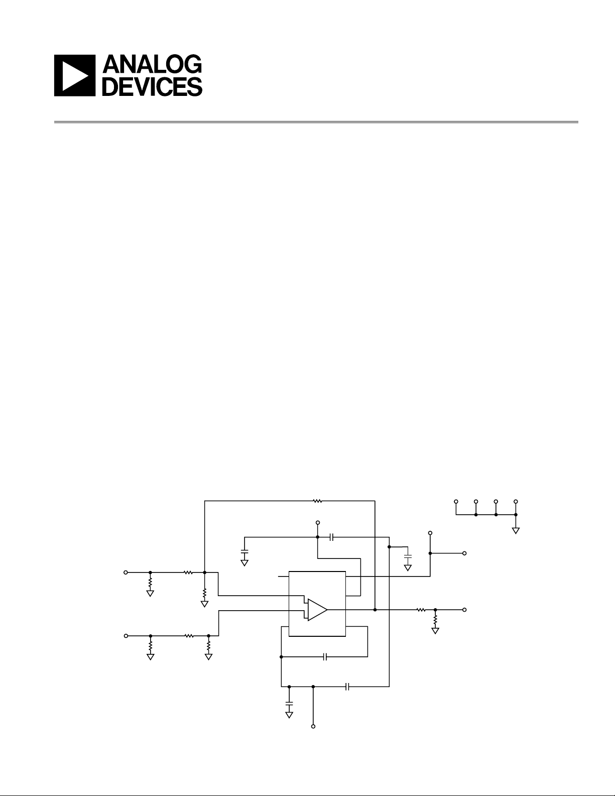
applications. Figure 1 shows the universal evaluation
board schematic.
The evaluation board is a 2- layer PCB that accepts SMA
connectors on the input and output for efcient connection to test equipment. The evaluation board can also
accommodate an SMA connector for the disable pin,
a feature found on Analog Devices’ op amps, such as
the AD8063AR and AD8027AR.
The ground plane, component placement, and supply
bypassing have been laid out to minimize parasitic
inductances and capacitances. The evaluation board’s
components are primarily SMT 1206 case size, with the
exception of the electrolytic bypass capacitors (C1, C4),
which are 3528 case size. The board can also be used
with op amps that utilize external frequency compensation capacitors, such as the AD8021AR.
There are two options for supply bypassing. The rst
is connecting additional shunt capacitors (C2, C5) in
parallel with the electrolytic capacitors (C1, C4) from
each supply to ground. This technique of power supply
bypassing provides wideband rejection of unwanted
noise on the supply lines. It is implemented by placing a
0 resistor in the C6 position and shunt capacitors in the
C1, C2, C4, and C5 positions.
The second approach connects one capacitor between
the supply rails. This method uses fewer components
and can improve the PSRR at higher frequencies. It is
implemented by inserting a 0 resistor in the C2 position, inserting the bypass capacitor in the C5 position,
and omitting C6. Optimal bypassing is circuit dependent
and therefore must be evaluated by the designer.
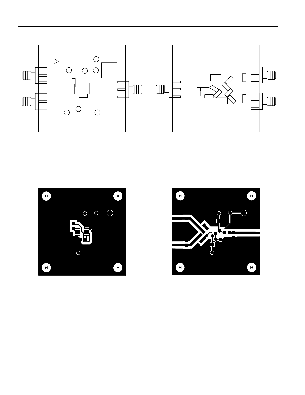
Figure 2 shows the evaluation board assembly drawing.
The recommended layout pattern for making connections
to the op amp and supporting circuitr y is shown in
Figure 3.
Figure 1. Universal Evaluation Board Schematic
REV. A
Page 2

AN-646
C1
R7
R4
R1
R9
R3
C2
C6
R8
C5
C4
R5
R2
DUT
DIS
OUT
OUT
R6
C3
UNIVERSAL HIGH SPEED
OP AMP EVALUATION BOARD
COMPONENT SIDE CIRCUIT SIDE
ANALOG
DEVICES
+VS
GND1
–VS
GND2
GND4
TP1
GND3
IN–
IN+
IN–
IN+
EVAL-ADOPAMP-1R
SO SINGLE
A00336C
*
*
*
* SMA EDGE CONNECTOR JOHNSON COMPONENTS, INC. P/N 142-0701-831
E03686–0–6/03(A)
Figure 2. Board Assembly Drawings
© 2003 Analog Devices, Inc. All rights reserved. Trademarks and registered trademarks are the property of their respective companies.
Figure 3. Board Layout Patterns
–2–
REV. A
 Loading...