

Page 1
AN-627
APPLICATION NOTE
One Technology Way • P.O. Box 9106 • Norwood, MA 02062-9106 • Tel: 781/329-4700 • Fax: 781/326-8703 • www.analog.com
AD5235 Evaluation Kit User Manual
by Alan Li
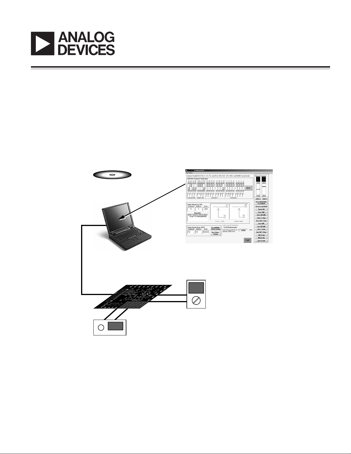
7 STEPS TO EVALUATION KIT SETUP
The AD5235 evaluation kit (AD5235EVAL25) consists of
a demonstration board and software for evaluating the
AD5235. It is a user-friendly tool that you can control
1.
INSTALL THE AD5235 SOFTWARE
2. INSTALL THE DRIVER
3. CONNECT THE PARALLEL
PORT CABLE
4. CONFIGURE THE
EVALUATION BOARD
with your personal computer through the printer port.
The driving program is self-contained, so no programming languages or skills are needed. Figure 1 provides
an overview of how to set up the kit.
H
AD5235
6. OPEN THE AD5235 SOFTWARE AND
PROGRAM THE RESISTANCE SETTINGS
REV. 0
+5V
5. APPLY THE POWER SUPPLY
GND
Figure 1. Evaluation Kit Setup
W1
B1
7. MEASURE THE RESULT
Page 2

AN-627
SETTING UP THE AD5235 EVALUATION BOARD
Step 1—Installing the AD5235 Software
To install the AD5235 software from the Revision H CD,
run setup.exe under D:\AD5235 Evaluation Software
Package. During the installation, select Ignore or Yes
to bypass error messages if they occur. You may need
to install the software a few times to get a successful
installation.
Step 2—Installing the Driver for PC Parallel Port Communications
In addition to installing the AD5235 software, you need
to install a third-party driver, NTPORT from Upper
Canada Technologies (UCT), for access to the PC parallel
port. UCT offers a free trial with a nominal license fee
after 30 days.
1. Download the driver from www.uct.on.ca. From the
UCT website, download NTPORT.OCX. Save
ntport.zip in the default or specified directory. Unzip
and extract all the files to the directory.
2. Run setup.exe. If the setup procedure indicates
file violations during installation, select Ignore to
bypass them.
3. Ensure that the driver file, dlportio.sys, is in the
correct system directory.
Note: If Windows® displays an error message, such as
“Can’t connect to service control manager,” contact the
IS department for authority to continue installation.
b.Change the pathname of the driver according to
the operating system.
• On a Windows 2000 or Window NT
enter c:\winnt\system32\drivers\dlportio.sys.
®
system,
• On a Windows XP system, enter
c:\windows\system32\drivers\dlportio.sys.
c. Click the Install button, then the Start button. If
the status message indicates success, the driver is
installed and operating. Click OK.
4. Set up the driver for automatic startup. Use the
following steps that apply to your operating system.
For Windows 2000 and XP Systems
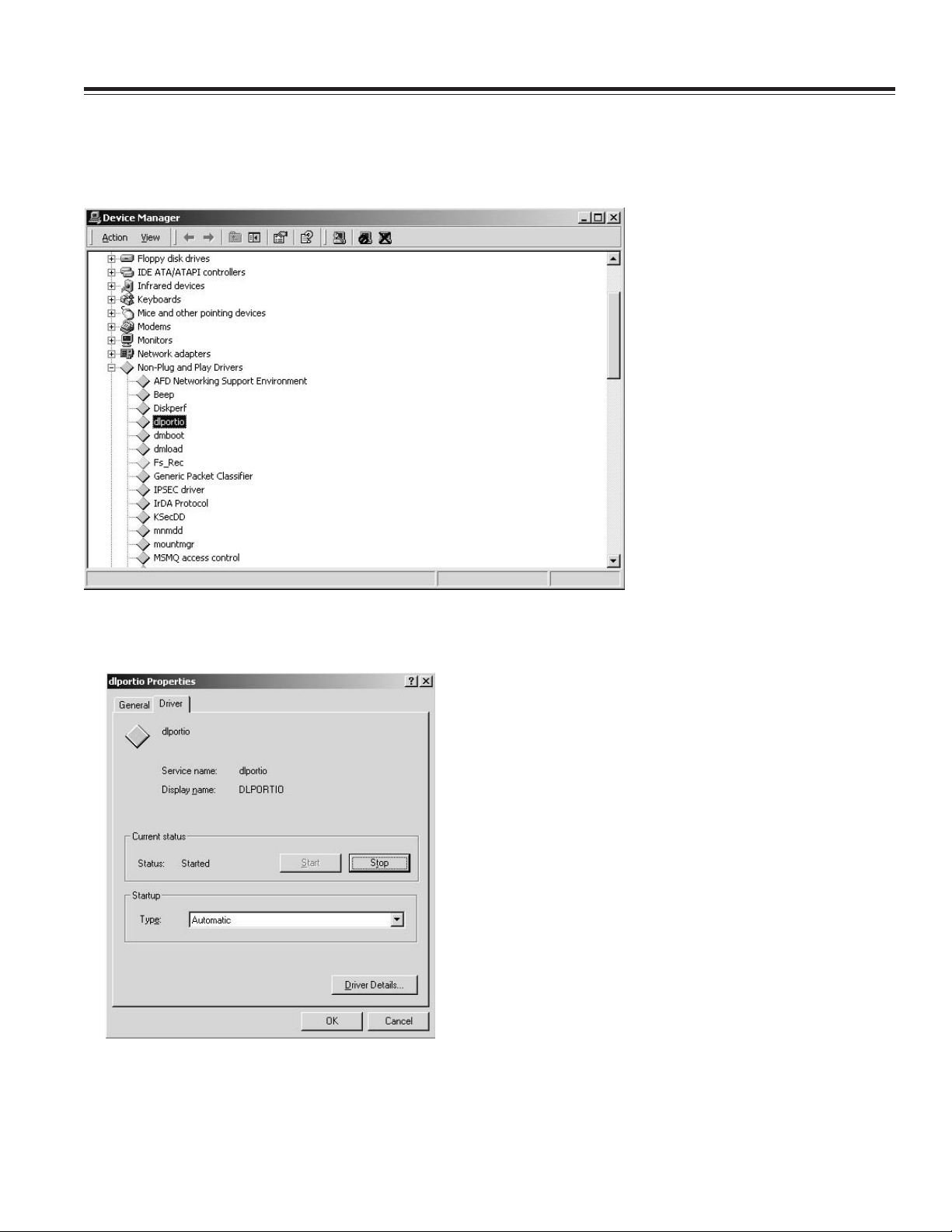
a. Go to the Device Manager.
• On a Windows 2000 system, click
Start → Settings → Control Panel → System →
Hardware → Device Manager.
• On a Windows XP system, click
Start → Control Panel → System → Hardware →
Device Manager.
a. Run loaddrv.exe under c:\program files\project1
or the specified directory. A dialog box appears.
–2–
REV. 0
Page 3
AN-627
b.Locate Non-Plug and Play Drivers and dlportio
in the Device Manager.
If the Non-Plug and Play Drivers entry is not visible, click the View menu in Device Manager and
select show Hidden Devices to make sure that
hidden driver files are listed. If you do not see
dlportio, reboot Windows or rerun loaddrv.exe and
then reboot Windows.
c. Double-click dlportio in the Non-Plug and Play
Drivers list. The dlportio Properties page appears.
d.At the Driver tab, select Startup Type as Auto-
matic, click Current status to Start, and click OK.
Note: If Startup is not active and you cannot change Type,
your computer may be administered by your IS department. You may need to consult them to change your PC
administrative setting.
REV. 0
–3–
Page 4
AN-627
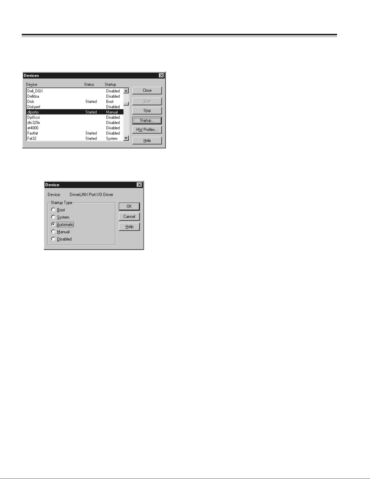
For Windows NT Systems
a. From the Windows NT Control Panel, select the
Devices icon. The Devices dialog box appears.
b.Select dlportio and click the Startup button. The
Device Startup Type dialog box appears. From the
option buttons, select Automatic, and then click OK.
• For dual supplies, connect JP15 and JP12 to connect
the –5 V pin to V
of U1 and U3.
SS
Warning: Apply +2.5 V to Pin +5 V and –2.5 V to
Pin –5 V instead.
• Select the states of PR and WP from the DIP switches
on the evaluation board.
• SDO can be monitored at TPSDO.
Step 5—Applying the Power Supply
Provide a power supply to the AD5235 evaluation
board according to Step 4 for a single supply or for
dual supplies.
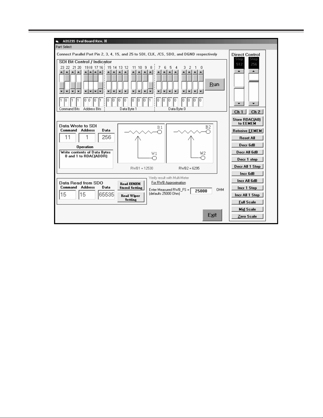
Step 6—Using the Evaluation Board
To open the AD5235 software program, from Windows
click Start → Programs → AD5235 Rev H.
Figure 2 shows the graphical interface. In the Direct Control pane, on the right, you can move the scroll bars or
click the buttons to control the device. In the top pane,
you can adjust the bit pattern and then click Run to program the device. In the bottom pane, you can
approximate R
R
after power is applied.
AB
and RWB by first entering the measured
WA
Step 7—Measuring the Result
Use a multimeter to measure the result of your program
applications on the AD5235 evaluation board.
Step 3—Connecting the Parallel Port Cable
Connect the parallel port cable from LPT1 on your PC to
the AD5235 evaluation board.
Step 4—Configuring the Evaluation Board
Follow these requirements to configure the AD5235
evaluation board:
• For a single supply, connect JP14 and JP13 to
ground V
of U1 and U3. Apply 5 V to Pin +5 V.
SS
Note: Some boards do not come with jumper
caps. You should supply suitable caps or simply
short the jumpers for proper operation.
UNINSTALLING SOFTWARE
To uninstall the AD5235 software and NTPORT driver,
use Add/Remove Programs in the Control Panel.
TECHNICAL SUPPORT
Due to the variations in computer platforms and configurations, Analog Devices, Inc., cannot guarantee the
software described in this application note to work on all
systems. If you encounter problems, send email to
digital.pots@analog.com or call 1-408-382-3082 for
applications support. If you are interested in the AD5235
source code, send email to alan.li@analog.com for more
information.
–4–
REV. 0
Page 5
AN-627
Figure 2. AD5235 Software Graphical Interface
REV. 0
–5–
Page 6
AN-627
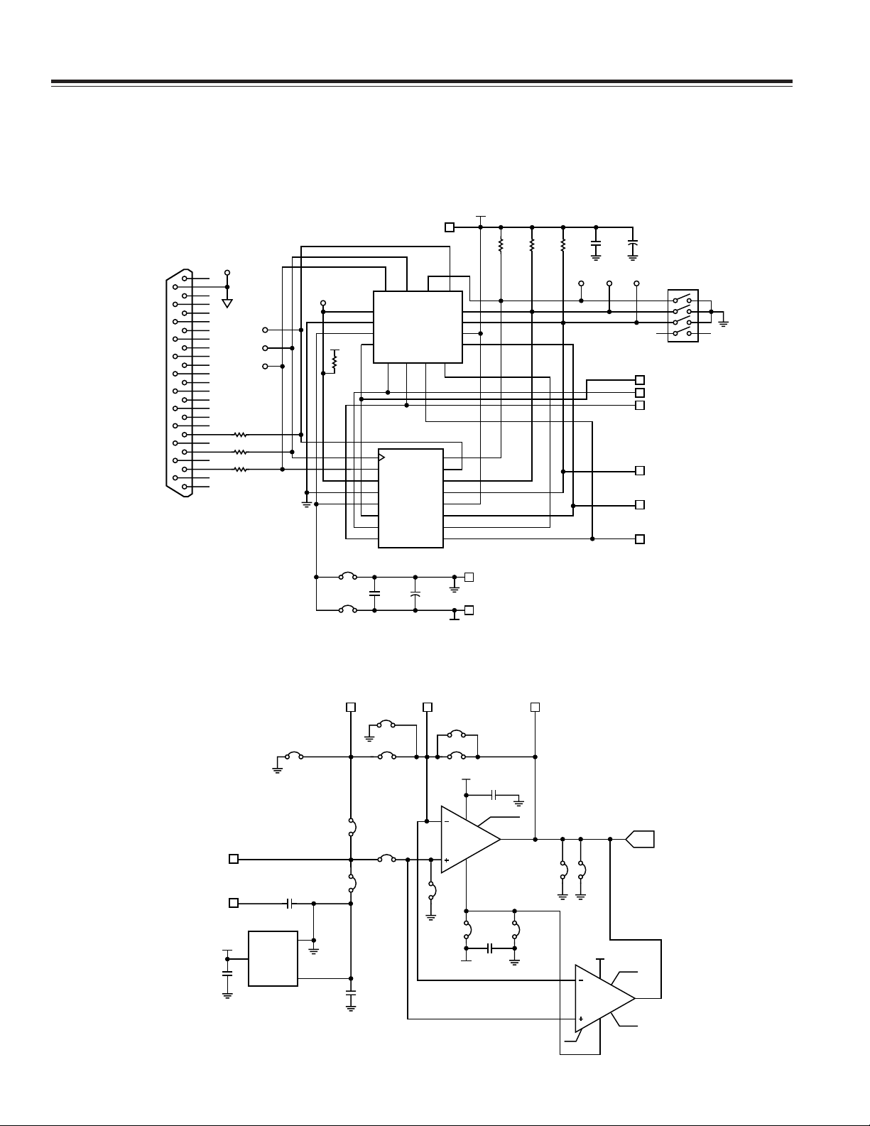
EVALUATION BOARD SCHEMATIC
The general-purpose op amp AD820, U3A can be configured
as various building block circuits in conjunction with the
AD5235 for various circuit evaluations (see the Applications
AD5235 MAIN CIRCUIT
J1
DB25
NOTES
USERS SHOULD IGNORE U1A, ADN2850CSP
SIGNAL GROUND WITH NET DGND
POWER GROUND WITH NET AGND
DGND
13
25
12
24
11
23
10
22
9
21
8
20
7
19
6
18
5
17
R_CS 100
4
16
R_CLK 100
3
15
R_SDI 100
2
14
1
TP/CS
TPCLK
TPSDI
ADN2850CSP
TPSDO
+5V
HEADER
HEADER
U1A
SDI16CLK15RDY14CS
1
SDO
2
GND
3
VSS
4
A1
R1
1k
1
2
3
4
5
6
7
8
JP14
JP15
(LOWER TO –2.5V IF DUAL SUPPLIES)
W15B16B2
SDI
SDO
GND
V
A1
W1
CLK
SS
7
RDY
CS
PR
WP
V
W2
B1
U1B
AD5235TSSOP
C12
C13
0.1F
4.7F
section). Other op amps in PDIP can replace the AD820. For a
single-supply, 2.5 V voltage reference, AD1582 can be
used to offset the op amp bias point for ac operation.
+5V
+5V
13
PR
WP
VDD
A2
W2
8
16
15
14
13
12
DD
11
A2
10
9
B2
–5V
(LOWER TO +2.5V IF DUAL SUPPLIES)
R2
R3
10k
10kR410k
12
11
10
9
GND
–5V
C10
4.7F
C11
0.1F
TP/WPTP/PRTPRDY
HIGH LOW
18
27
36
45
A1
W1
B1
A2
W2
B2
S1
SW-DIP4
VI_DC
V
_AC
I
0.1F
C7
ADDITIONAL OP AMP FOR GENERAL-PURPOSE APPLICATIONS
V+ V– V
+5V
3
AD1582
V
IN
HEADER
U2
GND
V
OUT
JP5
C9
HEADER
HEADER
2
1
2.5 VREF
JP4
JP3
JP7
JP6 JP8
JP2
HEADER
C8
0.1F
2
AD820AR
3
JP1
JP9
U3A
4
–5V
+5
7
C5
0.1F
1, 5, 8
JP12
HEADER
C6
0.1F
6
Figure 3. Evaluation Board Schematic
–6–
O
JP10 JP11
JP13
HEADER
2
AD820AN
3
1
+5V
7
U3B
REPLACEABLE
4
OP AMP IN PDIP
V
O
8
6
5
REV. 0
Page 7

AN-627
Table I. AD5235 24-Bit Serial Data-Word
MSB Instruction Byte 0 Data Byte 1 Data Byte 0 LSB
RDAC C3 C2 C1 C0 0 0 0 A0 X X XXXX D9D8D7D6D5D4D3D2D1D0
EEMEM C3 C2 C1 C0 A3 A2 A1 A0 D15 D14 D13 D12 D11 D10 D9 D8 D7 D6 D5 D4 D3 D2 D1 D0
Command bits are C0 to C3. Addresses bits are A3 to A0. Data bits D0 to D9 are applicable to the RDAC wiper register, whereas D0 to D15 are applicable
to the EEMEM register. Command instruction codes are defined in Table II.
Table II. AD5235 Instruction/Operation Truth Table
1, 2, 3
Instruction Byte 0 Data Byte 1 Data Byte 0
Instruction B23 • • • • • • • • • • • • • • • • • B16 B15 • • • B8 B7 • • • B0
No. C3 C2 C1 C0 A3 A2 A1 A0 X • • • D9 D8 D7 • • • D0 Operation
0 0000XXXX X • • • XX X • • •X NOP: Do nothing. See Table V.
1 0001000A0 X • • • XX X • • •X Write the contents of EEMEM(A0) to RDAC(A0). This
command leaves the device in the read program
power state. To return the device to the idle state,
perform NOP instruction 0. See Table V.
2 0010000A0 X • • • XX X • • •X Save wiper setting: Write the contents of RDAC(A0)
to EEMEM(A0). See Table IV.
4
3
0011A3A2A1A0 D15 • • • D8 D7• • • D0 Write the contents of serial register data bytes 0 and
1 (total 16-bit) to EEMEM(ADDR). See Table VII.
5
4
0100000A0 X • • • XX X • • •X Decrement 6 dB: Right-shift contents of RDAC(A0),
stops at all ”zeros.”
5
5
0101XXXX X • • • XX X • • •X Decrement all 6 dB: Right-shift contents of all RDAC
registers, stops at all ”zeros.”
5
6
0110000A0 X • • • XX X • • •X Decrement contents of RDAC(A0) by ”one,” stops at
all ”zeros.”
5
7
0111XXXX X • • • XX X • • •X Decrement contents of all RDAC registers by “one,”
stops at all “zeros.”
8 10000000 X • • • XX X • • •X Reset: Load all RDACs with their corresponding
EEMEM previously saved values.
9 1001A3A2A1A0 X • • • XX X • • •X Write contents of EEMEM(ADDR) to serial register
data bytes 0 and 1. SDO activated. See Table VIII.
10 1010000A0 X • • • XX X • • •X Write contents of RDAC(A0) to serial register data
bytes 0 and 1. SDO activated. See Table IX.
11 1011000A0 X • • • D9D8D7 • • •D0Write contents of serial register data bytes 0 and 1
(total 10 bit) to RDAC(A0). See Table III.
5
12
1100000A0 X • • • XX X • • •X Increment 6 dB: Left-shift contents of RDAC(A0),
stops at all “ones.” See Table VI.
5
13
1101XXXX X • • • XX X • • •X Increment all 6 dB: Left-shift contents of all RDAC
registers, stops at all “ones.”
5
14
1110000A0 X • • • XX X • • •X Increment contents of RDAC(A0) by “one,” stops at
all “ones.” See Table IV.
5
15
1111XXXX X • • • XX X • • •X Increment contents of all RDAC registers by “one,”
stops at all “ones.”
NOTES
1
The SDO output shifts out the last 24 bits of data clocked into the serial register for daisy-chain operation. Exception: For any instruction following
instruction 9 or 10, the selected internal register data will be present in data byte 0 and 1. The instructions following 9 and 10 must also be a full 24-bit
data-word to completely clock out the contents of the serial register.
2
The RDAC register is a volatile scratchpad register that is refreshed at power-on from the corresponding nonvolatile EEMEM register.
3
Execution of the above operations takes place when the CS strobe returns to logic high.
4
Instruction 3 writes two data bytes (total 16 bit) to EEMEM. However, in the cases of addresses 0 and 1, only the last 10 bits are valid for wiper position setting.
5
The increment, decrement, and shift commands ignore the contents of the shift register data bytes 0 and 1.
REV. 0
–7–
Page 8

AN-627
PROGRAMMING EXAMPLES
The following programming examples illustrate the
typical sequence of events for various features of the
AD5235. Refer to Table II for the instructions and dataword format. The instruction numbers, addresses, and
data appearing at the SDI and SDO pins are displayed in
hexadecimal format in the tables.
Table III. Scratchpad Programming
SDI SDO Action
B00100HXXXXXXHLoads data 100H into the RDAC1
register. Wiper 1 moves to the
1/4 full-scale position.
B10200
H
B00100
Loads data 200H into the RDAC2
H
register. Wiper 2 moves to the
1/2 full-scale position.
Table IV. Incrementing RDAC Followed
by Storing the Wiper Setting to EEMEM
SDI SDO Action
B00100HXXXXXXHLoads data 100H into the RDAC1
register. Wiper 1 moves to the
1/4 full-scale position.
E0XXXX
H
B00100
Increments the RDAC1 register
H
by one to 101H.
E0XXXX
E0XXXXHIncrements the RDAC1 register
H
by one to 102H.
Continue until the desired wiper
position is reached.
20XXXXHXXXXXXHSaves RDAC1 register data into
EEMEM1.
Optionally tie WP to GND to
protect EEMEM values.
Table V. Restoring EEMEM Values to RDAC Registers
SDI SDO Action
10XXXXHXXXXXXHRestores EEMEM1 value to
RDAC1 register.
00XXXXH10XXXXXHNOP. Recommended step to
minimize power consumption.
8XXXXXH00XXXXHResets EEMEM1 and EEMEM2
values to RDAC1 and RDAC2
registers, respectively.
EEMEM values for RDACs can be restored by power-on, strobing the
PR pin or programming as shown above.
Table VI. Using Left Shift by One to Increment 6 dB Steps
SDI SDO Action
C0XXXXHXXXXXXHMoves wiper 1 to double the
present data contained in the
RDAC1 register.
C1XXXX
C0XXXXHMoves wiper 2 to double the
H
present data contained in the
RDAC2 register.
Table VII. Storing Additional User Data in EEMEM
SDI SDO Action
32AAAAHXXXXXXHStores data AAAAH into spare
EEMEM location USER1. Allowable to address in 13 locations
with maximum 16 bits of data.
335555
32AAAAHStores data 5555H into spare
H
EEMEM location USER2. Allowable to address 13 locations
with maximum 16 bits of data.
Table VIII. Reading Back Data from
Various Memory Locations
SDI SDO Action
92XXXXHXXXXXXHPrepares data read from USER1
location.
00XXXXH92AAAAHNOP instruction 0 sends 24-bit
word out of SDO where the last
16 bits contain the contents of
USER1 location. NOP command
ensures device returns to idle
power dissipation state.
Table IX. Reading Back Wiper Setting
SDI SDO Action
B00200HXXXXXXHSets RDAC1 to midscale.
C0XXXX
B00200HDoubles RDAC1 from midscale
H
to full scale.
A0XXXX
C0XXXXHPrepares reading wiper setting
H
from RDAC1 register.
XXXXXXHA003FFHReads back full-scale value
from RDAC1 register.
–8–
REV. 0
Page 9

APPLICATIONS
V
R1 R2RDAC
I
–R2
(R1 + R
AN-627
U1
AD5235
1
CLK
2
SDI
3
SDO
4
GND
5
V
SS
6
BA
V
O
A1*
7
W1
8
B1
JP15
–5V (–2.5V)
) V
AB
R1 V
I
I
VI_DC
1
VI_AC
C9
1
–(R2+RAB)
< VO <
Figure 4. Inverting Gain and Attenuator
JP3
RDY
CS
PR
WP
V
DD
A2*
W2
B2
–INPUT
16
15
14
13
12
11
10
9
R1
EXTERNAL
R2
EXTERNAL
V
O
1
+5V (+2.5V)
1, 5, 8
7
2
1
U3
AD820AR
3
JP1
4
JP12
6
V
O
0V
–200mV
0 0.5
V(VO)
V
= 100mV
I
R1 = RDAC = R2 = 10k
POTSETTING
1.0
–5V (–2.5V)
RDAC
U1
AD5235
1
CLK
SDI
SDO
GND
V
SS
A1*
W1
B1
RDY
CS
PR
WP
V
A2*
W2
B2
DD
2
3
4
5
V
R
I
A
R
V
O
6
7
8
B
–1 < V
O
VI < 1
A2* (SIGNAL INPUT HERE)
1
16
15
14
FB
13
1
12
11
10
9
R
EXTERNAL
JP4
JP2
–INPUT
1
R
JP8
+5V (+2.5V)
2
U3
AD820AR
3
1V
= 1V
V
V
O
1, 5, 8
7
6
I
–1V
00.5
V(VO)
V
O
POTSETTING
1.0
4
JP12
–5V (–2.5V)
Figure 5. Bipolar Unity Gain Amplifier
U1
AD5235
1
CLK
SDI
SDO
GND
V
SS
A1*
W1
B1
RDY
CS
PR
WP
V
A2*
W2
B2
2
3
4
5
D1
I
S
R
RDAC
R1
A
B
V
O
6
7
8
JP15
–5V (–2.5V)
VO = –k R I
k = 1 +
S
R
R
WB
WB
+
R1
R
16
15
14
13
12
DD
11
10
9
FB –INPUT
1 1
R1
JP7
R
JP6
VI_DC
1
D1
+5V (+2.5V)
2
AD820AR
3
JP1
–5V (–2.5V)
1.2V
V
O
1
1, 5, 8
7
U3
6
V
O
IS = 10nA
R = 100k
RDAC = 10k
R1 = 10
0V
0 0.5
V(VO)
1.0
POTSETTING
4
JP12
Figure 6. High Sensitivity I-V Coverter
REV. 0
–9–
Page 10

AN-627
V
IN
A
RDAC
B
V
R1 RDAC
I
G =
VO =
–R
WB
R1
(D RAB)
–V
I
(2
BA
n
R1)
U1
AD5235
1
CLK
2
SDI
3
SDO
4
GND
5
V
SS
6
A1*
7
W1
8
V
O
B1
JP4
RDY
CS
PR
WP
V
A2*
W2
B2
16
15
14
13
12
DD
11
10
9
A
1
FB
1
5V
= 5V
V
I
R
= 10k
AB
JP2
+5V (+2.5V)
JP4
JP2
2
AD820AR
3
1, 5, 8
7
U3
6
4
0V
0 0.5
V(VO)
V
O
1.0
POTSETTING
JP12
–5V (–2.5V)
Figure 7. Buffered Output Voltage
U1
AD5235
1
CLK
2
SDI
3
SDO
4
GND
5
V
SS
6
A1*
7
W1
8
V
O
B1
JP15
–5V (–2.5V)
VI_DC
16
RDY
15
CS
14
PR
13
WP
12
–INPUT
V
DD
11
10
9
JP4
R1
JP6
1
2
3
+5V (+2.5V)
7
U3
AD820AR
4
A2*
W2
B2
1
JP1
JP12
1, 5, 8
V
O
1
6
V
O
0V
–200mV
0 0.5
V(VO)
= 0.1V
V
I
R1 = 5k, R
POTSETTING
AB
= 10k
1.0
–5V (–2.5V)
Figure 8. Inverting Linear Gain and Attenuator
U1
AD5235
1
CLK
2
SDI
3
SDO
4
GND
5
V
SS
V
I
RDAC
BA
V
O
6
A1*
7
W1
8
B1
JP15
–5V (–2.5V)
–R
WB
G =
R
WA
VO = V
D
I
2n –
1
RDY
CS
PR
WP
V
DD
A2*
W2
B2
VI_DC
VI_AC
16
15
14
13
FB
–INPUT
1
12
11
10
9
1
V
O
1
–10V
V
I
R
= 0.1V
= 10k
AB
JP4
–100V
1
JP3
C9
1
+5V (+2.5V)
2
AD820AR
3
JP1
1, 5, 8
7
U3
6
V
O
4
JP12
0 0.5
V(VO)
POTSETTING
1.0
–5V (–2.5V)
Figure 9. Inverting Quasi Log Gain and Attenuator
–10–
REV. 0
Page 11

AN-627
RDAC
V
I
BA
G =
R
VO =
R1 RDAC
V
I
R
G = 1 +
R1
VO = VI 1+
R2
–R2
WA
(2n R2)
–V
I
n
– D) R
(2
BA
WB
D R
2n R1
RDY
CS
PR
WP
V
A2*
W2
FB
1
16
15
14
13
–INPUT
12
DD
11
10
9
B2
C9
JP4
JP3
1
2
3
R2
JP8
+5V (+2.5V)
7
U3
AD820AR
4
JP1
JP12
1, 5, 8
V
O
1
–10V
V
= 0.1V
I
= 10k, R2 = 10k
R
AB
LOG
–100mV
6
V
O
00.5
V(VO)
POTSETTING
1.0
V
O
AB
JP15
–5V (–2.5V)
U1
AD5235
1
CLK
2
SDI
3
SDO
4
GND
5
V
SS
6
A1*
7
W1
8
B1
VI_DC
1
VI_AC
1
–5V (–2.5V)
Figure 10. Inverting Exponential Gain and Attenuator
U1
AD5235
1
CLK
2
SDI
3
SDO
4
GND
5
V
SS
6
A1*
7
W1
8
V
O
B1
JP14
VI_DC
AB
1
JP5
RDY
WP
V
A2*
W2
CS
PR
B2
DD
JP2
16
15
14
13
12
11
10
9
JP6
R1
–INPUT
1
2
AD820AR
3
+5V
U3
V
O
1
1, 5, 8
7
6
300mV
= 0.1V
V
I
R1 = 5k, RAB = 10k
0V
0 0.5
V
O
V(VO)
POTSETTING
1.0
4
RDAC
V
I
G = 1 +
V
BA
= VI 1+
O
JP13
Figure 11. Noninverting Linear Gain
RDY
V
A2*
C9
CS
PR
WP
W2
B2
GND
1
16
15
14
13
12
DD
–INPUT
11
1
10
9
V
O
1
10V
V
R
= 0.1V
I
= 10k
AB
+5V
1, 5, 8
7
JP2
2
AD820AR
3
U3
6
4
100mV
0 0.5
V
O
V(VO)
POTSETTING
1.0
JP3
JP13
U1
AD5235
1
CLK
2
SDI
3
SDO
4
GND
5
V
SS
6
A1*
7
W1
8
V
O
B1
JP14
R
WB
R
WA
D
n
– D
2
VI_DC
1
_AC
V
I
1
Figure 12. Noninverting Quasi Log Gain
REV. 0
–11–
Page 12
AN-627
RDAC
BA
V
I
R2
R2
G = 1 +
R
WA
VO = VI 1 +
V
O
n
(2
n
R2
2
– D) R
GND
RDY
WP
V
A2*
W2
C9
CS
PR
DD
B2
1
16
15
14
13
–INPUT
12
11
10
9
1
R2
JP8
V
O
1
+5V
1, 5, 8
7
2
6
V
O
4
JP2
AD820AR
3
U3
10V
V
= 0.1V
I
RAB = 10k , R2 = 10k
100mV
0 0.5
V(VO)
1.0
POTSETTING
JP3
JP13
U1
AD5235
1
CLK
2
SDI
3
SDO
4
GND
5
V
SS
6
A1*
7
W1
8
B1
JP14
VI_DC
1
AB
VI_AC
1
Figure 13. Noninverting Exponential Gain
+2.5V
R1
1M, 0.1%
A
RDAC
B
R2
1M, 0.1%
–2.5V
R
VW = V+ – V–
R2 + R
WB
AB
U1
AD5235
1
CLK
SDI
SDO
GND
V
SS
A1*
W1
B1
RDY
CS
PR
WP
V
DD
A2*
W2
B2
2
3
4
5
6
7
8
V
O
JP15
–5V (–2.5V)
–5V (–2.5V)
R
WA
R1 + R
AB
Figure 14. Ultrafine Adjustment
+5V (+2.5V)
16
15
14
13
12
11
10
9
R2
R1
EXTERNAL
–INPUT
+5V (+2.5V)
2
3
JP1
JP8
7
U3
AD820AR
4
JP12
–5V (–2.5V)
1, 5, 8
V
O
6
V
O
–12–
REV. 0
Page 13
V
I
RDAC
R1 R2
A
B
RDAC
C1
G = 180 – 2tan^ – 1wRC
VA
A
B
V
REF
VB
AN-627
U1
AD5235
1
CLK
2
SDI
3
SDO
4
GND
5
V
SS
6
A1*
7
W1
8
V
O
B1
JP15
–5V(–2.5V)
U1
AD5235
1
CLK
2
SDI
3
SDO
4
GND
5
V
SS
6
A1*
7
W1
8
V
O
B1
JP15
–5V(–2.5V)
16
RDY
15
CS
14
PR
13
WP
12
V
A2*
W2
DD
11
10
9
B2
–INPUT
R1
EXTERNAL
FB
JP4
JP2
3
VI_AC
1
Figure 15. Phase Shifter
16
RDY
15
CS
14
PR
13
WP
+5V(+2.5V)
12
V
DD
11
A2*
10
W2
9
B2
JP4
2
JP2
3
JP8
+5V(+2.5V)
2
U3
AD820AR
C1
JP1
–5V(–2.5V)
JP8
+5V(+2.5V)
7
U3
AD820AR
4
R2
7
4
JP12
1, 5, 8
1, 5, 8
V
O
6
V
O
2.0V
)
V(V
I
–2.0V
0s 100s 200s 300s
V(VO)
TIME
5.0V
VA = V+ = +2.5V
VB = V– = –2.5V
= 0V
V
REF
6
V
O
–5.0V
0 0.5 1.0
V(VO)
POTSETTING
Figure 16. Level Detector
JP13
REV. 0
–13–
Page 14
AN-627
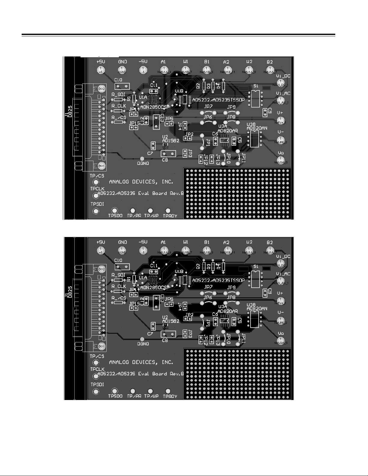
PCB LAYOUT
Figure 17. Evaluation Board PCB Layout
Figure 18. Top Layer
–14–
REV. 0
Page 15

AN-627
Figure 19. Bottom Layer
REV. 0
Figure 20. Top Overlay Silkscreen
–15–
Page 16

AN-627
PCB LAYOUT CONSIDERATIONS
To stabilize voltage supplies, bypass Pin +5 V and Pin –5 V
with a 4.7 µF or 10 µ F capacitor with proper polarities. Adding 0.1 µF decoupling capacitors, very close to
the supply pins of the active component, can minimize
high frequency noise as well.
Table X. PCB Parts List
Designator Footprint Comment
TPSDO Test point 0.09
TPCLK Test point 0.09
TPSDI Test point 0.09
TP/CS Test point 0.09
+5 V Post pin 0.125
GND Post pin 0.125
B1 Post pin 0.125
W1 Post pin 0.125
A1 Post pin 0.125
_DC Post pin 0.125
V
I
VI_AC Post pin 0.125
C9 RAD 0.1
A2 Post pin 0.125
W2 Post pin 0.125
B2 Post pin 0.125
–5 V Post pin 0.125
VO Post pin 0.125
V– Post pin 0.125
V+ Post pin 0.125
JP8 Jumper 0.3
JP9 Jumper 0.3
JP7 Jumper 0.3
JP6 Jumper 0.3
JP1 Jumper 0.3
JP11 Jumper 0.3
JP10 Jumper 0.3
Designator Footprint Comment
TPRDY Test point 0.09
TP/WP Test point 0.09
TP/PR Test point 0.09
DGND DGNDPAD
C12 RAD 0.1 0.1 µF
C7 RAD 0.1 0.1 µF
C11 RAD 0.1 0.1 µF
C6 RAD 0.1 0.1 µF
C5 RAD 0.1 0.1 µF
R_/CS Axial 0.3 100 Ω
R_CLK Axial 0.3 100 Ω
R_SDI Axial 0.3 100 Ω
R4 Axial 0.3 10 kΩ
R3 Axial 0.3 10 kΩ
R2 Axial 0.3 10 kΩ
R1 Axial 0.3 1 kΩ
C8 RAD 0.2 1 µF
C13 RAD 0.2 4.7 µF
C10 RAD 0.2 4.7 µF
U2 SOT-23 AD1582
U1B TSSOP-16 AD5235TSSOP
U1A LFCSP-16 ADN2850CSP
5 mm × 5 mm
U3B DIP8 AD820AN
U3A SO-8 AD820AR
J1 DB25SL DB25
JP15 SIP2 Header
JP14 SIP2 Header
JP5 SIP2 Header
JP3 SIP2 Header
JP2 SIP2 Header
JP4 SIP2 Header
JP12 SIP2 Header
JP13 SIP2 Header
S1 DIP8 SW-DIP4
–16–
REV. 0
Page 17

PR CS CLK SDI
AN-627
GND
13 12 11 10
25
24
S7 S6 S5 S4 S3
NOTES
8 OUTPUT PINS ACCESSED VIA THE DATA PORT
5 INPUT PINS (1 INVERTED) ACCESSED VIA THE STATUS PORT
4 OUTPUT PINS (3 INVERTED) ACCESSED VIA THE CONTROL PORT
REMAINING 8 PINS ARE GROUNDED
D7 D6 D5 D4 D3 D2 D1 D0
23 22921820719618
4 321
5
17 16 14
15
C3 C2 C1 C0
SDO
(NTPORT1.ADDRESS = 888)
(NTPORT1.ADDRESS = 889)
(NTPORT1.ADDRESS = 890)
Figure 21. Parallel Port Connector Configuration (For VB Program Developers Only)
PR
BIT 3
(PIN 5)
CS
BIT 2
(PIN 4)
CLK
BIT 1
(PIN 3)
SDI
BIT 0
(PIN 2)
BINARY CODE
DECIMAL CODE
11001210019101111100081010
10
SEND OUT
NO ACTIVITY LATCH DATA
BIT_TOGO = 1
SEND OUT
BIT_TOGO = 0
1100
12
Figure 22. Timing Definition (For VB Program Developers Only)
REV. 0
–17–
Page 18

–18–
Page 19

–19–
Page 20

AN03554–0–3/04(0)
© 2004 Analog Devices, Inc. All rights reserved. Trademarks and registered trademarks are the property of their respective owners.
–20–
 Loading...