Page 1

AN-620
APPLICATION NOTE
One Technology Way • P.O. Box 9106 • Norwood, MA 02062-9106 • Tel: 781/329-4700 • Fax: 781/326-8703 • www.analog.com
Using the AD1836 and AD1953 for a 4-In/9-Out
Analog System with DSP
By Jerad Lewis
The AD1953 is a member of Analog Devices’ SigmaDSP™
family of parts and includes a 3-channel, differential- output
DAC and integrated audio DSP. This DSP can be used for
equalization, dynamics processing, stereo spreading, and
other audio processing. The AD1836 is a multichannel audio
codec that includes four ADCs and six DACs, all in a fully differential confi guration. Together, these two parts can easily
be used to implement a 4-in/9-out system with DSP.
This two-chip setup is useful in applications that require
a mix of digital and analog inputs and a large number of
analog outputs, such as an automobile. The two stereo
analog inputs to the AD1836’s ADCs could be connected
to an AM/FM radio and cassette tape deck, and the digital
inputs of the AD1953 3:1 mux could be connected to a
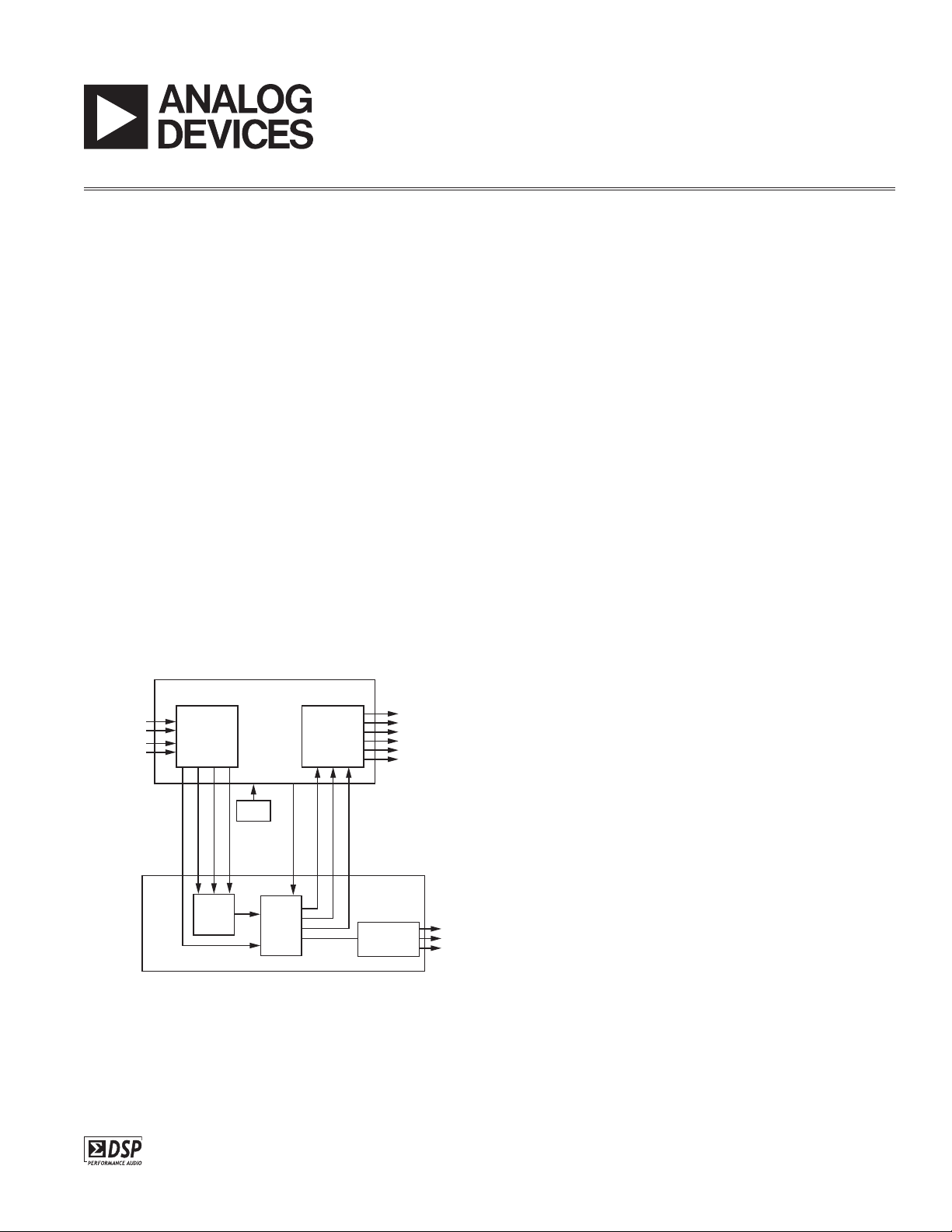
combination of the ADC output (as shown in Figure 1),
CD player, DVD player, or digital radio. This way, the source
of the DSP can be easily selected with the AD1953 control
registers.
AD1836
PAIR OF
STEREO
ANALOG
INPUTS
AUX
DATA
INPUT
4-CHANNEL
ADC
ASDATA2
ASDATA1
INPUT
MUX
AD1953
ABCLK
ALRCLK
MCLK
AUDIO
DSP
6-CHANNEL
MCLK
TDM DATA
DAC
TDM BCLK
TDM FRAME SYNC
3-CHANNEL
DAC
Figure 1. Functional Block Diagram
The dynamic range of the ADCs is 105 dB; the DACs have
a dynamic range of 112 dB on the AD1953 and 108 dB on the
AD1836. Even if the AD1953’s digital volume control is
set to a comfortable listening level of –15 dB, this still
allows for a dynamic range of 90 dB through the whole
signal path.
The digital inputs to the AD1953 come from the two serial
data outputs of the AD1836’s ADCs and other I
2
S compatible sources. In the case where both ADC data outputs are
sent to the AD1953, one of these stereo digital signals is
sent to the AD1953 input mux and the other is sent to the
auxiliary data input. The AD1953 includes a time division
multiplexed (TDM) output mode that can be used to send
up to six channels of data to the AD1836 DACs over a
single data line. At the same time, the AD1953’s three onboard DACs can be used for a total of nine analog output
channels. Figure 1 shows a functional block diagram of
the connections between the two chips.
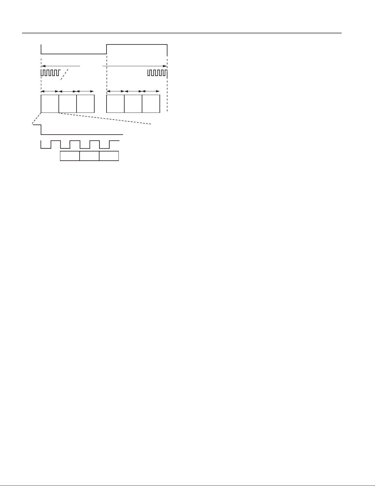
The TDM signal in this application can pack up to six channels of digital audio data into one sample period (21 ms
at 48 kHz sampling rate). This higher data rate is achieved
by increasing the bit clock rate from 64f
to 256fs. On
s
the AD1836, this TDM input mode is called DAC Packed
Mode 256. The AD1836 is put into this mode by writing
to the serial mode bits in DAC Control Register 1, and the
AD1953 is set to TDM output in Control Register 1. A timing
diagram of the TDM mode is shown in Figure 2. The TDM
frame sync signal is low for the fi rst 128 BCLKs and high
for the fi nal 128 BCLKs. Each data slot is 32 BCLKs wide
and is formatted in an I
2
S-like manner (MSB delayed one
BCLK from the start of the frame). The signals output in
the TDM stream are selected by writing to the AD1953’s six
data capture serial out registers (Registers 268-273). The
AD1953 data sheet details the format of an SPI write to
set these registers. The ADCs and DACs of the AD1836 and
AD1953 can handle a full 24-bit audio signal at a maximum
sampling frequency of 48 kHz. All registers are set through
the respective chips’ SPI control port.
REV. 0
The AD1953 is a member of ADI’s
SigmaDSP™ family of parts.
Page 2

AN-620
LRCLKO/
TDMFS
256BCLKs
BMUXO/
TDMBC
32BCLKs
LRCLK
BCLK
DATA
32BCLKs32BCLKs
DMUXO/
TDMO
32BCLKs
SLOT 0
32BCLKs
SLOT 1
MSB
32BCLKs
SLOT 2 SLOT 3 SLOT 4 SLOT 5
MSB–1 MSB–2
Figure 2. TDM Format Timing Diagram
The system’s master clock is generated from a 12.288 MHz
(256 ⫻ f
) oscillator that is connected to the AD1836. The
s
master ADCs provide two lines of serial data, a bit clock,
and an L/R clock. These two serial data lines run off these
common clocks. The TDM data and clocks, including the
TDM bit clock and TDM frame sync, are provided via the
serial output port of the AD1953.
The AD1953 may be used with either its default DSP program or a custom program designed using a simple
graphical compiler. Using the graphical compiler,
SigmaComposer, the user can completely reconfi gure
the program and parameter RAM of the chip to a desired
signal processing fl ow. SigmaComposer works by placing
signal processing blocks, such as biquad fi lters, mixers,
delays, and dynamics processors, in a schematic and wiring
the blocks together. The compiler engine then takes this
schematic and creates a program and a parameter fi le to
load into the chip.
EVALUATION BOARD SETUP AND CONNECTIONS
The AD1836 and AD1953 evaluation boards have convenient 20-pin headers to easily connect a ribbon cable
between them. This cable carries the clocks and signals
from the ADCs to the DSP and sends the 6-channel TDM
signal back to the AD1836 DACs.
When SW2 of the AD1953 evaluation board is set to
Position B, ASDATA1 is sent to all three mux inputs of the
AD1953, and ASDATA2 is sent to the AUXDATA input. SW3
on the AD1953 board should be set to the proper data
format that is being output from the ADCs. LK9 must be set
to Position B; this routes the AD1836 evaluation board
master clock to MCLK0 of the AD1953. The AD1836 evaluation board mode switch (SW3) should be set to Position F.
More information about evaluation board setup and
operation can be found in the respective evaluation board
data sheets.
After the AD1953’s data capture registers are set, the data
will be output on the TDM stream to the AD1836 DACs.
TDM Slot 0 corresponds to AD1836 DAC 1, Slot 1 is sent
to AD1836 DAC 2, and so on.
E03304–0–4/03(0)
© 2003 Analog Devices, Inc. All rights reserved. Trademarks and registered trademarks are the property of their respective companies.
–2–
REV. 0
 Loading...