Page 1

9106
www.analog.com
word rate. It contains two differential analog input chan-
to power down the device between conversions, which
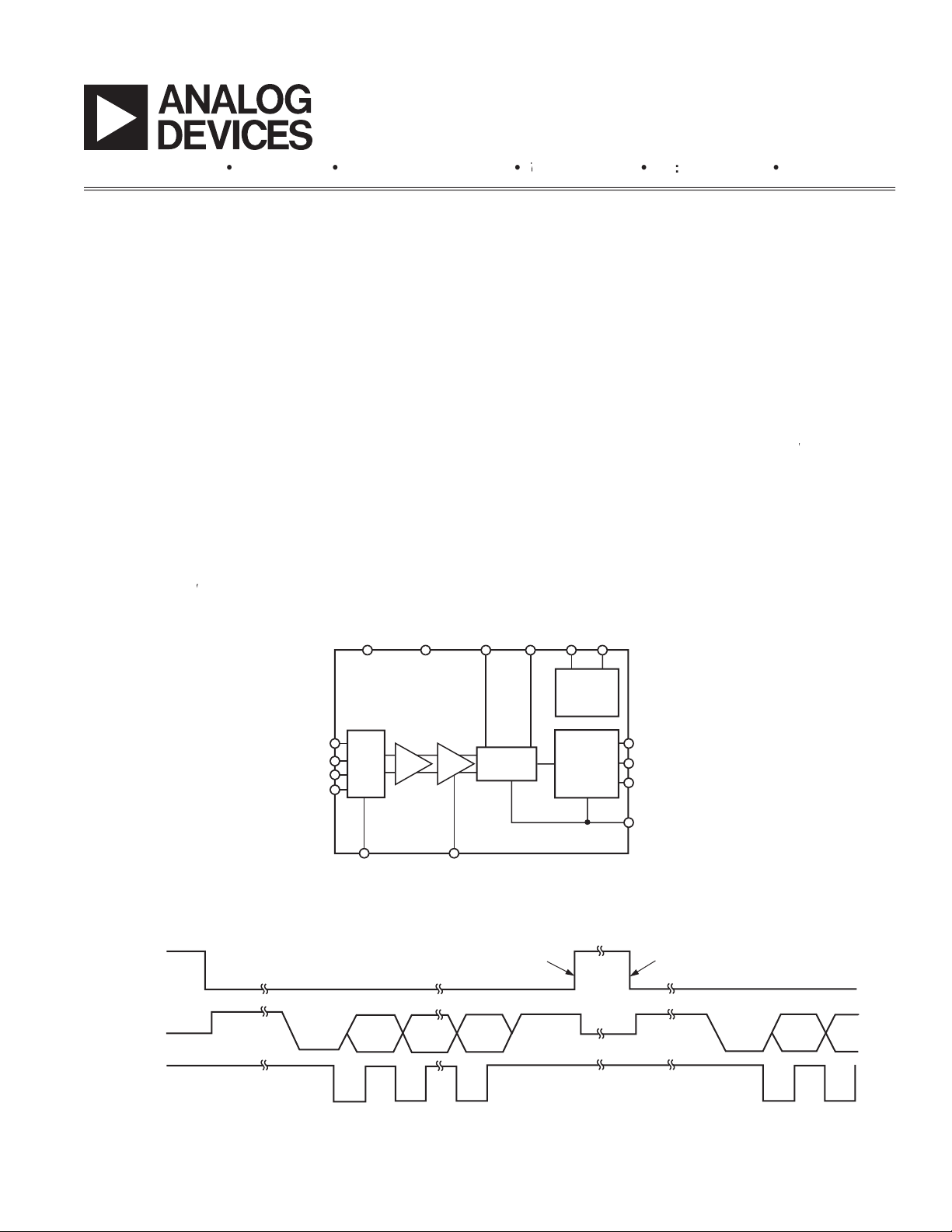
As shown in Figure 1, the AD7782 has a 3-wire serial
CS
AIN1(+)
AIN1(–)
AIN2(+)
AIN2(–)
CH1/CH2 RANGE
AD7782
V
DD
GND
BUF PGA
REFIN(–)REFIN(+)
MUX
24-BIT -
ADC
OSCILLATOR
AND
PLL
DOUT/RDY
SCLK
MODE
XTAL1 XTAL2
SERIAL
INTERFACE
AND
CONTROL
LOGIC
CS
will continuously convert with an update rate of 19.79 Hz.
CS
pin operates as a power-down pin as well as
CS
is high, continu-
RDY
becomes
three-stated, the AD7782 enters standby mode, and any
CS
goes low, the phase locked loop
then begins converting the selected channel.
MSB
DOUT/RDY
SCLK
AD7782 IS POWERED DOWN
CS
LSB
MSB
AD7782 IS POWERED UP
SCLK IS AN INPUT IN SLAVE MODE AND AN OUTPUT IN MASTER MODE.
Page 2

–2
–
tered trademarks are the property of their respective companies.
When the AD7782 is powered up, it consumes 1.3 mA
typical at 3 V and 1.5 mA typical at 5 V. In power-down
typical at 5 V. By placing the AD7782 in power-down
CS
until the next conversion is required.
As seen in Figure 2, taking
CS
low powers up the AD7782.
After power-up, the ADC requires some time to settle
to convert. The sigma-delta ADC uses chopping, which
RDY
will remain high until a
valid conversion result is available. With an update rate
the AD7782 must remain powered-up for (2
50.5) +
Assuming a 3 V power supply, the average current equals
6) + (0.102
1300) = 138 µA.
With a 5 V power supply and, again, with one conversion
20) +
1500) = 171 µA.
functions in which the part performs one conversion each
6) + (0.00002833
1300) =
With a 5 V power supply, the average current equals
20) + (0.00002833
1500) = 20.04 µA.
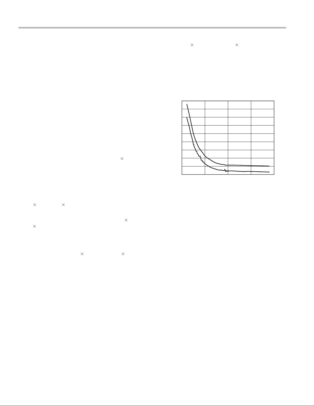
which the ADC performs a single conversion, the AD7782
version. From the plot, the average current approaches
the power-down current speci cation when the time inter-
val between conversions is 15 seconds or greater.
3V
CONVERSION RATE – Minutes
180
0
0.01 1000.1
CURRENT – A
1 10
20
160
140
120
100
80
60
40
5V
CS
operates as both a chip-
ADC between conversions does not add additional
 Loading...