Page 1

9106
www.analog.com
voltages and other low frequency errors. This Applica-
tion Note outlines how chopping is implemented on the
AD7708/AD7718, AD7709, AD7719, AD7782/AD7783 high
ADCs and discusses the resulting bene ts
thermocouple voltage that arises when two dissimilar
An offset that arises within the various ampli ers
modulator can generally be nulled out,
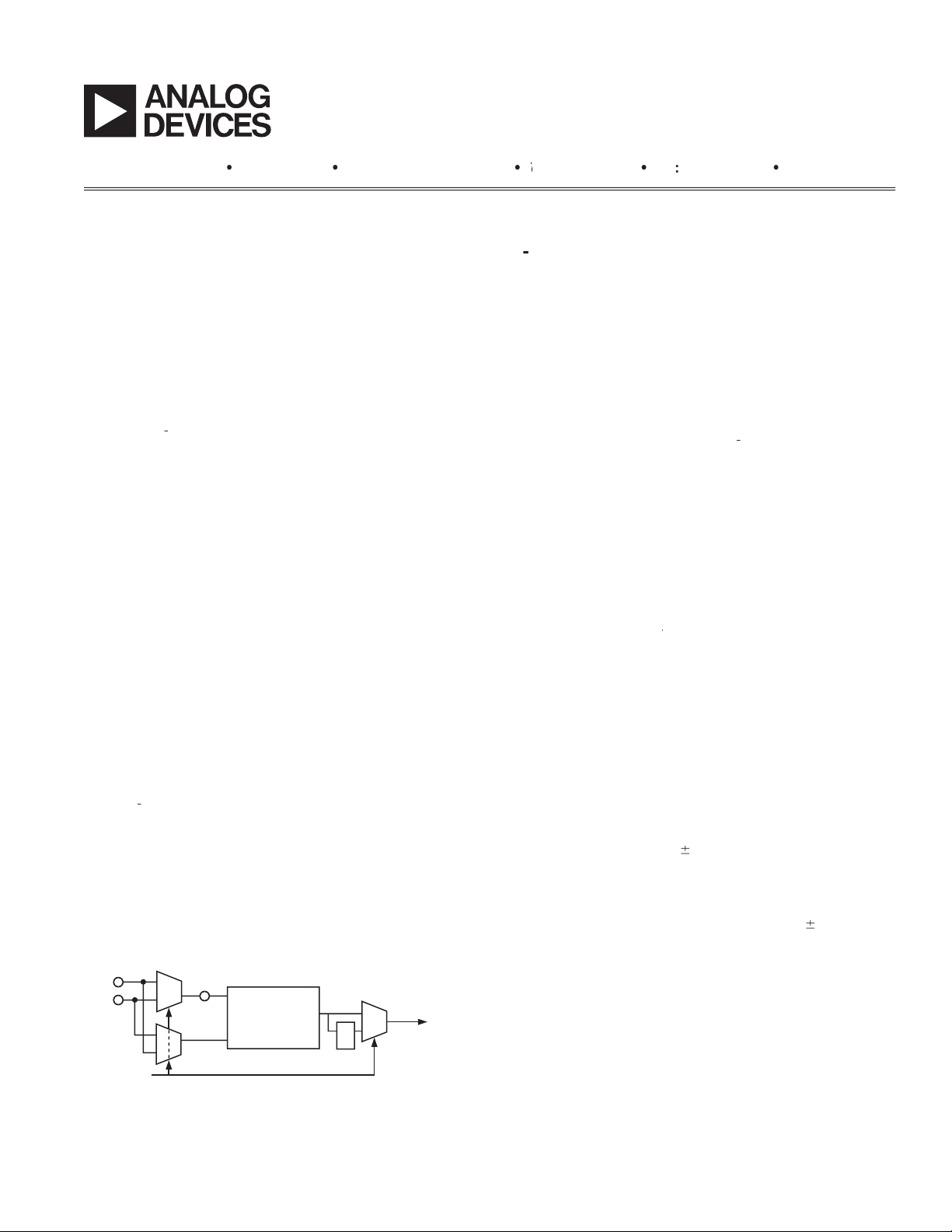
to chop the entire analog signal chain within the ADC.
AIN(+)
AIN(–)
–
+
V
OS
0
1
0
1
INPUT MUX
CHOP
VIN(+)
VIN(–)
- MODULATOR
TO
DIGITAL
FILTER
OUTPUT MUX
–1
0
1
modulator as a term
added to the input signal, then the output when
A A V
IN IN OS
+
( ) ( )
( )
+– –
– – –A A V
IN IN OS
( )
+
( )
( )
+
[ ]
two results in the digital lter, leaving:
A A
IN IN
+
( ) ( )
( )
– –
which equals the differential input voltage without any
within the ADC, and, more importantly, to minimize
ADCs is speci ed as
virtually unmeasurable. The entire analog circuitry is
ADC offset calibrations are therefore not required.
ADC
ADC
ADCs
Page 2

–2
–
there are no intermediate/invalid outputs produced––the
rst output after a channel change is 100% settled to the
to the ADC, for example, if a sensor output changes
a change has occurred. It will
when the external mux is switched, then restarting the
ADC so it produces an output 2
ADC
later.
lter, for a period of time the output will re ect a combi-
1.2
1.0
0.8
0.6
0.4
0.2
0
V
IN
V
OUT
ADCs contain a low-pass FIR lter with
nite duration impulse/step response.
the average of the current ADC conversion and the previ-
ADC conversion period, then the current ADC conversion
will re ect a combination of the old analog input and
the new input, and the averaged result will be an inter-
with the previous conversion. it will not yet give the nal
value, so it produces the second unsettled output. Only
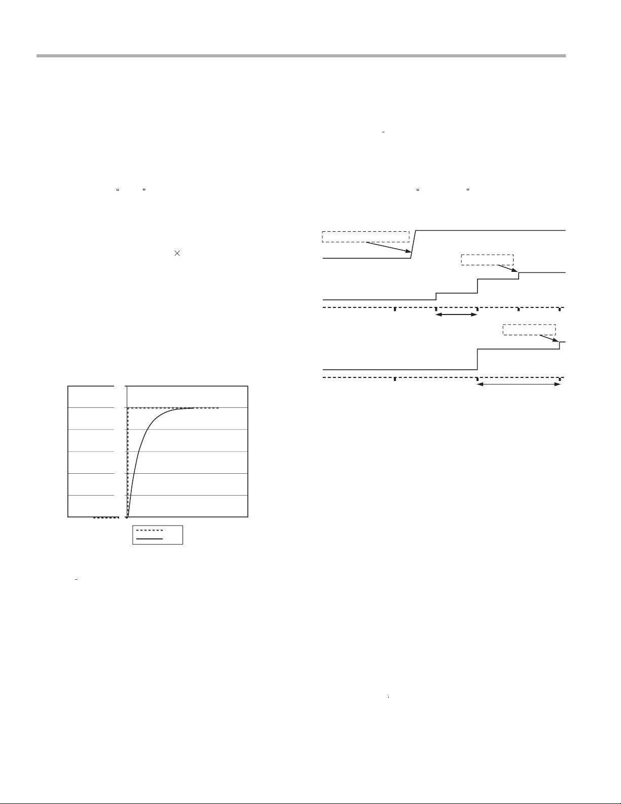
the third output will be fully settled (see Figure 3 (i)).
ADCs restrict the ADC to producing out-
ADC
throughput. In this case there is at most one intermediate
ADC conversion rate (see Figure 3 (ii)). This has been
but in fact such ADCs
these ADCs from Analog Devices.
CHANGE IN ANALOG INPUT
ADC INPUT
ADC OUTPUT (i)
ADC OUTPUT (ii)
FULLY SETTLED
FULLY SETTLED
T
ADC (i)
T
ADC
(ii)
Which scheme is the best? In most applications the need
to get information as fast as possible is most important.
you get an indication that a reaction is going to overheat,
the sooner corrective action can be taken.
With faster outputs from the ADC, there is an earlier
ADC
ADC
later. But if the input
/2, which can provide improved 50 Hz/60 Hz
/2, which can provide improved 50 Hz/60 Hz
Page 3

–3
–
the latency response of
ADCs, so this Application
Page 4

–4
–
 Loading...