Page 1

AN-605
a
APPLICATION NOTE
One Technology Way • P.O. Box 9106 • Norwood, MA 02062-9106 • Tel: 781/329-4700 • Fax: 781/326-8703 • www.analog.com
Synchronizing Multiple AD9852 DDS-Based Synthesizers
by David Brandon
INTRODUCTION
Many applications require the generation of two or
more sinusoidal or square wave signals with a known
phase relationship between them. The AD9852 DDS IC
from Analog Devices is capable of providing such signals. This application note offers detailed instructions
on how to synchronize two or more of these devices and
considers possible sources of phase error. For a quadrature application, see the AD9854 DDS with its built-in
quadrature configuration; however, this application
note would also apply to the AD9854 as well.
For successful synchronization, the user must have control over the timing relationship between REFCLK and
the rising edge of the EXT I/O UPDATE CLK. The goal is
to have all DDSs operating on the same SYSTEM CLK
count and not off by ±1 or more counts from each DDS.
Therefore, the EXT I/O UPDATE CLK must be made synchronous with the REFCLK.
REFCLK
OPTIMUM LAYOUT
A = B = C
REFCLK
A
C
DDS NO.1
B
DDS NO. 3
DDS NO. 1
DDS NO. 2
DDS NO. 3
DDS NO. 2
For phase errors due to DAC output filtering mismatches, the AD9852 features programmable phase
adjust that can null out these types of mismatches.
REF CLOCK
The first requirement for successful synchronization of
multiple AD9852s is that there must be minimal phase
error between the REFCLK inputs to all DDSs. Any difference in-phase between the REFCLK edges will result in a
proportional phase difference at the DDS outputs.
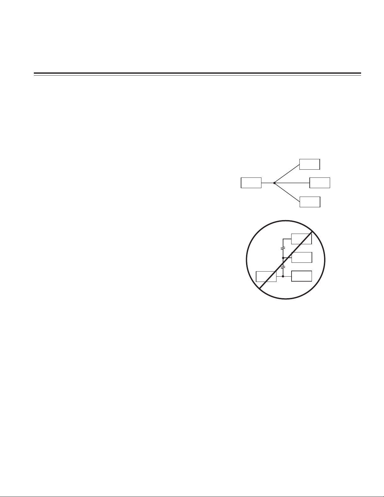
Therefore, the user must employ a careful clock distribution practice in the layout of the PCB (see Figure 1).
The AD9852 REFCLK input circuitry has an option of
using differential inputs or a single-ended configuration.
Differential REFCLK mode is recommended for its optimum switching characteristics. The REFCLK edges
should have minimum input jitter and fast rise/fall times
(less than 1 ns is recommended). A slow rise time on
REFCLK can increase the phase error time because the
voltage trip point of the input circuit varies from
device to device.
REV. 0
Figure 1. REFCLK Distribution
I/O UPDATE CLOCK
The I/O UPDATE CLK is responsible for transferring the
contents of the I/O port buffer to the programming
registers where the data becomes active. This clock
has two modes of operation in which the DDS can
supply the I/O UPDATE CLK, or the user can supply it.
For synchronization reasons, external mode is highly
recommended. Internal mode was not given consideration for complexity reasons.
AD9852 I/O INTERFACE DETAILS
Once a fast-edged and properly routed REFCLK signal is
provided, the next timing requirement is the coincident
transfer of the data into the DDS programming registers.
The I/O UPDATE CLK transfers the contents of the I/O
port buffer to the programming registers where data
becomes active. Synchronization of multiple DDSs
requires that the EXT I/O UPDATE CLK’s rising edge
occur simultaneously at all DDSs, just like the REFCLK.
In addition, the rising edge of the EXT I/O UPDATE CLK
must occur at the proper time with respect to REFCLK.
© 2003 Analog Devices, Inc.
Page 2

AN-605
The AD9852 can be programmed in serial or parallel
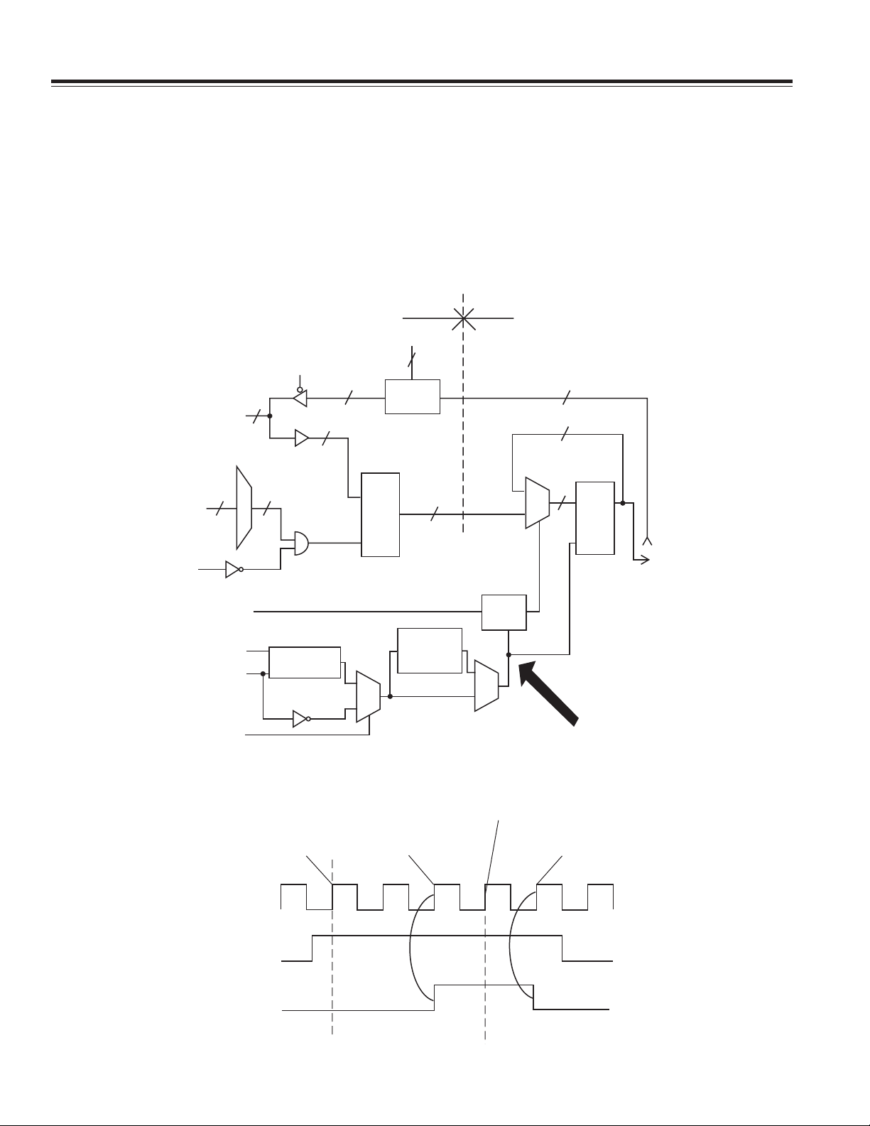
mode. Figure 2 depicts the parallel mode. If shown, the
serial mode would display an additional 7-bit shift register and other support circuitry in front of the parallel
data path. However, the main reason for showing this
diagram is to view the paths of REFCLK and EXT I/O
UPDATE CLK.
A few things to note in Figure 2 are how the SYSTEM
CLK is derived and the inversion of REFCLK in singleended REFCLK mode. Also note, an asynchronous EXT
I/O PORT BUFFERS
RD
8
8
ADDRESS
WR
DATA
6
D
E
40
C
O
D
E
1 OF 40
8
1 OF 40
L
D
A
T
C
H
EN
ADDRESS
6
READBACK
MUX
I/O UPDATE CLK will be made synchronous to the SYSTEM
CLK via the edge detection circuitry (see Figure 3). However, it is incumbent upon the user to make it
synchronous with the REFCLK to avoid a SYSTEM CLK
count mismatch between DDSs.
Depending on the setting of the REFCLK mode (singleended or differential) and/or the use of the on-chip
REFCLK multiplier (PLL), the timing relationship
between REFCLK and EXT I/O UPDATE CLK will change.
These timing changes will be addressed later.
PROGRAMMING
REGISTERS
320
8
8
8
UPDATE REGS
(SEE TIMING FOR
EDGE DETECT BELOW)
0
M
U
X
1
1 OF 40
DQ
F/F
CK
DDS
EXT
I/O UPDATE
CLOCK
REFCLKB
REFCLK
DIFF/SINGLE
FIRST SYSTEM TO SEE
EXT I/O UPDATE CLK
SYSTEM CLK
EXT I/O UPDATE CLK
UPDATE REGS
EDGE
DETECT
REFCLK
M
U
X
MULTIPLIER
0
M
U
X
1
DIFFERENTIAL
MODE
1
0
SYSTEM CLOCK
Figure 2. AD9852 Parallel Interface Block Diagram
I/O PORT BUFFERS CONTENTS
ARE REGISTERED INTO
PROGRAMMING REGISTERS
FORMS RISING EDGE
OF UPDATE REGS
0
1
2
3
FORMS FALLING EDGE
OF UPDATE REGS
Figure 3. Ext I/O Update CLK's Edge Detect Timing
–2–
REV. 0
Page 3

AN-605
From the timing in Figure 3, it is essential that a proper
time relationship exist between EXT I/O UPDATE CLK
and the SYSTEM CLOCK for synchronization to occur. If
this time relationship is met, then all SYSTEM CLOCKs
are on the same count across all DDSs and not off by ±1
or more SYSTEM CLOCK counts. The user would control
this relationship with the control of the rising edge of the
EXT I/O UPDATE CLK with respect to the REFCLK. This
timing relationship will be addressed in the SYNCHRONIZATION INSTRUCTIONS section.
RESET—BACKGROUND
A RESET must be given after power-up and prior
to transferring any data to the DDS. This places the
DDS output into a known phase, which becomes the
common reference point that allows the synchronization
of multiple DDSs.
RESET forces the AD9852’s phase accumulator state to
become COS(0). When new data is sent simultaneously
to multiple DDSs, a coherent phase relationship can be
maintained, or the relative phase offset between
multiple DDSs can be predictability shifted by means of
the phase offset adjustment register. The AD9852 has
14 bits of phase-offset adjustment that amounts to
a phase resolution of 0.022°. The phase-offset feature is
located between the phase accumulator and the phaseto-amplitude converter.
SYNCHRONIZATION INSTRUCTIONS
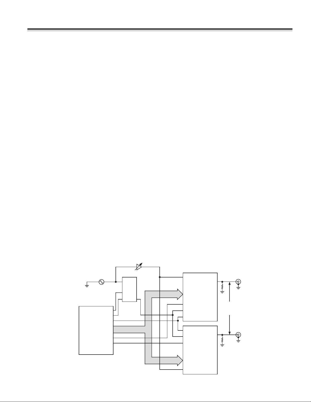
Figure 4 presents one possible reference design for
the successful synchronization of multiple DDSs. This
example shows how to place two DDSs into the same
phase relationship.
In Figure 4, the D flip-flop enables the EXT I/O UPDATE
CLK to be synchronous with the REFCLK and provides a
setup time. Proper operation may require additional
time delay in the REFCLK path. This delay
depends on the CK–to–Q propagation time of the flipflop. The recommended timing relationship between the
EXT I/O UPDATE CLK (Pin 20) and the REFCLK (Pin 69) is
depicted in Figures 5 and 6, depending on single-ended
or differential REFCLK mode. Timing for the REFCLK
multiplier enabled is depicted in Figures 8 and 9.
Here are some general instructions and recommendations for placing two DDSs into the same phase
relationship (refer to Figure 4).
Note that there are two sets of instructions, with and
without the REFCLK multiplier enabled.
Instructions (without the AD9852’s REFCLK multiplier
enabled) to synchronize two DDSs.
1. Power up all devices and apply the common REFCLK.
2. Send a common RESET with a minimum high time
of 10 REFCLK periods.
3.
Program all DDSs for EXT I/O UPDATE CLK mode
(bypass digital multipliers and inverse sync, if desired).
4. Program DDS No. 1 to the desired frequency and a
phase offset of 0°
without
issuing an EXT I/O
UPDATE CLK.
5. Program DDS No. 2 to the exact same frequency
and a
phase offset of 0° without issuing an EXT I/O
UPDATE CLK.
REV. 0
THREE STATE
EXT I/0 UPDATE CLK
RESET
MICROPROCESSOR
OR FPGA
WRB NO.1
WRB NO.2
DELAY
CK
D FLOP
EN
Q
D
DATA/ADDRESS BUS
Figure 4. Application Circuit
–3–
REFCLK
AD9852 NO. 1
DATA/ADDRESS
WRB
EXT I/O UPDATE CLK
RESET
RESET
EXT I/O UPDATE CLK
WRB
AD9852 NO. 2
DATA/ADDRESS
REFCLK
ZERO
PHASE
DIFFERENCE
Page 4

AN-605
REFCLK (PIN 69)
EXT I/O UPDATE CLK MUST
OCCUR WITHIN THIS RANGE
EXT I/O
UPDATE CLK (PIN 20)
NOTE: EXT I/O UPDATE CLK'S RISING EDGE TIMING IS RELATIVE TO REFCLK'S RISING EDGE.
0.5ns
VA LI D
AVOID THESE WINDOWS OF
TIME WITH RESPECT TO THE
RISING EDGE OF THE EXT
I/O UPDATE CLK AND THE
RISING EDGE OF REFCLK
1.2ns
Figure 5. Proper Timing Relationship between REFCLK and EXT I/O Update CLK in Differential REFCLK Mode
EXT I/O UPDATE CLK MUST
OCCUR WITHIN THIS RANGE
REFCLK (PIN 69)
EXT I/O
UPDATE CLK (PIN 20)
VA LI D
0.3ns
AVOID THESE WINDOWS OF
TIME WITH RESPECT TO THE
RISING EDGE OF THE EXT
I/O UPDATE CLK AND THE
FA LLING EDGE OF REFCLK
NOTE: EXT I/O UPDATE CLK'S RISING EDGE TIMING IS RELATIVE TO REFCLK'S FALLING EDGE.
THIS IS DUE TO THE INVERSION OF THE REFCLK IN SINGLE-ENDED MODE. SEE FIGURE 2 FOR INVERSION.
1.5ns
Figure 6. Proper Timing Relationship between REFCLK and EXT I/O Update CLK in Single-Ended REFCLK Mode
6. See the diagrams above for the recommended
timing between EXT I/O UPDATE CLK and REFCLK.
Choose the appropriate diagram given differential
or single-ended REFCLK mode.
7. Assert a
common
EXT I/O UPDATE CLK. This will
result in the DAC outputs becoming active simultaneously at the correct frequency and phase offset
as programmed.
interval is not predictable. Therefore, the tuning word
must be zero during this time period, which is the
default if preceded with a RESET. A tuning word of zero
prevents the phase accumulator from incrementing
while the PLL locks.
Since all the devices are clocked by a common REFCLK
and the PLLs are phase locked to REFCLK, all SYSTEM
CLK signals should also be in-phase, assuming a proper
REFCLK signal is routed to each DDS as discussed
USING THE REFCLK MULTIPLIER (PLL) ON THE AD9852
The REFCLK multiplier of the AD9852 must be used with
care when synchronizing multiple DDSs because the
PLL lock time will vary from device to device.
This means that the number of SYSTEM CLK cycles
delivered to the phase accumulator during the PLL lock
previously.
A typical PLL lock time is approximately 400 µs. Due to
variations in IC processing and temperature effects on
lock time, it is recommended to allow at least 1.0 ms for
locking to occur (refer to Figure 7).
–4–
REV. 0
Page 5

AN-605
TEK STOP: 1.00MS/s
PLL LOCK TIME
DAC OUTPUT
2
3
CH1
CH3 1.00V⍀
EXT I/O UPDATE CLK
50.0mV⍀ M 50s CH3 700mV
CH21100.0mV⍀
VCO INPUT
Figure 7. Typical PLL Lock Time
REFCLK (PIN 69)
⌬: 378s
@: –101s
0.3ns
@ 300MSPS OR ELSE REFER
1.5ns
EXT I/O UPDATE CLK
MUST OCCUR WITHIN THIS
RANGE IF SYSTEM CLK IS
TO T HE NOTE BELOW
Note: The REFCLK multiplier will lock to the falling edge
of REFCLK; therefore, the EXT I/O UPDATE CLK signal
should be referenced to the falling edge of REFCLK in
differential REFCLK mode and to the rising edge in
single-ended mode. The recommended timing relationship between the rising edge of the EXT I/O UPDATE
CLK (Pin 20) and the REFCLK (Pin 69) is depicted in Figures 8 and 9.
EXT I/O
UPDATE CLK (PIN 20)
@300MSPS
THE EDGE CAN BE MOVED
TO THE LEFT PROPORTIONALLY
SYSTEM CLK FREQUENCY
NOTE: THE RISING EDGE OF EXT I/O UPDATE CLK IS RELATIVE TO THE FALLING EDGE OF REFCLK DUE TO THE FACT THAT THE PLL LOCKS TO THE FALLING EDGE OF REFCLK.
0.3ns
SYSTEM CLK FREQUENCY
WITH A DECREASE IN
VA LI D
NOTE: THE VALID TIMING
RANGE WILL INCREASE
WITH A DECREASE IN THE
THE EDGE IS FIXED AS THE
OUTER LIMIT FOR
I/O UPDATE CLK
(MAX 1.8ns FROM FALLING
EDGE OF REFCLK)
Figure 8. Proper Timing Relationship Using the REFCLK Multiplier in Differential REFCLK Mode
1.8ns
EXT I/O UPDATE CLK MUST
OCCUR WITHIN THIS RANGE
IF SYSTEM CLK IS @ 300MSPS
OR ELSE REFER TO THE
NOTE BELOW
0.3ns
REFCLK (PIN 69)
EXT I/O
UPDATE CLK (PIN 20)
@ 300MSPS
0.3ns
VA LI D
NOTE: THE VALID TIMING
RANGE WILL INCREASE
WITH A DECREASE IN
SYSTEM CLK FREQUENCY
REV. 0
THE EDGE CAN BE MOVED
TO THE LEFT PROPORTIONALLY
WITH A DECREASE IN
SYSTEM CLK FREQUENCY
THE EDGE IS FIXED AS THE
OUTER LIMIT FOR
I/O UPDATE CLK
(MAX 1.5ns FROM RISING
EDGE OF REFCLK)
Figure 9. Proper Timing Relationship Using the REFCLK Multiplier in Single-Ended REFCLK Mode
–5–
Page 6

AN-605
CH4
50.0mV⍀ M 25ns CH3
2.08V
2.00V⍀
3
1
⌬: 123.0ns
@: 119.0ns
DDS NO.2 OUTPUT
EXT I/O UPDATE
DDS NO.1 OUTPUT
2
T
T
FTW1S
CH1
CH3 2.00V⍀
CH2
4
50.0mV⍀
LATENCY THROUGH
DEVICE GIVEN THE
CONFIGURATION
(INV SINC AND DIG
MULT BYPASSED)
300MHz REFERENCE CLOCK (NON-PLL MODE)
INSTRUCTIONS WITH THE AD9852’S REFCLK MULTIPLIER ENABLED TO SYNCHRONIZE TWO DDSs.
1. Power up all devices and apply the common REFCLK.
2. Send a common RESET with a minimum high
time of 10 REFCLK periods.
3. Program all DDSs for EXT I/O UPDATE CLK mode
(bypass digital multipliers and inverse sync, if desired).
4. Program all DDSs for PLL mode along with the
REFCLK multiplier value.
5. Send a EXT I/O UPDATE CLK and wait 1.0 ms for
PLLs to lock.
6. Program DDS No. 1 to the desired frequency and a
phase offset of 0°
without
issuing an EXT I/O
UPDATE CLK.
7. Program DDS No. 2 to the exact same frequency
and a phase offset of 0° without issuing an EXT
I/O UPDATE CLK.
8. See the diagrams below for the recommended
timing between EXT I/O UPDATE CLK and
REFCLK. Choose the appropriate diagram for dif
ferential or single-ended REFCLK mode.
IMPORTANT: Users must remember to keep the REFCLK
multiplier enabled as they write each new tuning word
and/or phase offset.
9. Assert a common EXT I/O UPDATE CLK. This will
result in the DAC outputs becoming active simultaneously at the correct frequency and phase offset
as programmed.
SUMMARY
With proper care and procedure, synchronization can be
achieved among multiple DDSs. The following illustrations show how two AD9852s are synchronized to one
another. In Figure 10, the REFCLK frequency is set to
100 MHz, and in Figure 11, it is 300 MHz. Both are in nonPLL mode. For Figure 12, REFCLK is set to 75 MHz with
the REFCLK multiplier programmed for 43 (System
Clock = 300 MHz). Figure 13 shows two DDSs remaining
in quadrature, even as the frequency changes are made.
Quadrature is denoted by the cursor positioning in
Figure 13.
⌬: 370ns
DDS NO.1 OUTPUT
DDS NO.2 OUTPUT
T
FTW1S
LATENCY THROUGH
2
DEVICE GIVEN THE
CONFIGURATION
(INV SINC AND DIG
MULT BYPASSED)
T
EXT I/O UPDATE
3
1
100MHz REFERENCE CLOCK
(NON-PLL MODE)
4
50.0mV⍀ M 100ns CH3
CH1
CH3 2.00⍀
CH2
CH4
50.0mV⍀
2.00V⍀
@: 366ns
1.88V
Figure 10. DDS Synchronization – (Conditions: VCC = 3.3 V,
REFCLK = 100 MHz, Non-PLL Mode, 25ºC)
Figure 11. DDS Synchronization – (Conditions: VCC = 3.3 V,
REFCLK = 300 MHz, Non-PLL Mode, 25ºC)
–6–
REV. 0
Page 7

AN-605
DDS NO.1 OUTPUT
DDS NO.2 OUTPUT
T
2
T
EXT I/O UPDATE
3
75MHz REFERENCE CLOCK (PLL MODE 4ⴛ = 300MHz)
1
4
CH2
50.0mV⍀ M 25ns CH3
CH1
CH3 2.00V⍀
CH4
50.0mV⍀
2.00V⍀
⌬: 123.0ns
@: 118.5ns
2.08V
Figure 12. DDS Synchronization – (Conditions: VCC = 3.3 V,
REFCLK = 75 MHz, PLL (4⫻) Mode Enable, 25ºC)
⌬: 1.13s
@: 1.64s
T
T
2
CH1
100mV⍀ M 500ns CH4
CH2
2.70V100mV⍀
Figure 13. DDS Quadrature Synchronization – (Conditions:
= 3.3 V, REFCLK = 40 MHz, Non-PLL Mode, 25ºC)
V
CC
REV. 0
–7–
Page 8

E03074–0–1/03(0)
–8–
PRINTED IN U.S.A.
 Loading...