

Page 1
AN-587
a
One Technology Way • P.O. Box 9106 • Norwood, MA 02062-9106 • Tel: 781/329-4700 • Fax: 781/326-8703 • www.analog.com
APPLICATION NOTE
Synchronizing Multiple AD9850/AD9851 DDS-Based Synthesizers
by David Brandon of Analog Devices, Inc.
INTRODUCTION
Many applications require the generation of two or
more sinusoidal signals with a known phase relationship (e.g., quadrature). The AD9850 and AD9851 DDS
ICs from Analog Devices are capable of providing such
signals. This application note offers detailed instructions on how to synchronize two or more of these
devices, and considers possible sources of phase error.
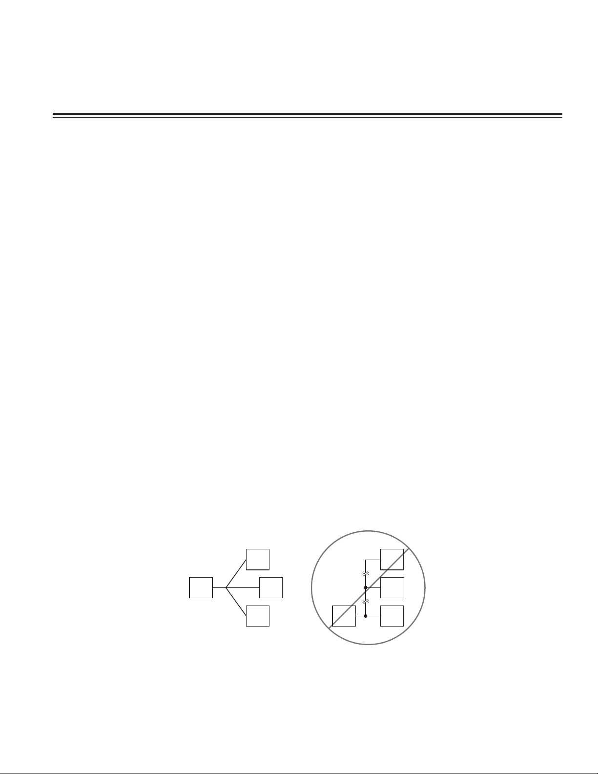
REF CLOCK
The first requirement for successful synchronization of
multiple AD9850/AD9851s is that there must be minimal
phase error between the REF CLK inputs to all DDSs.
Any difference in phase between REF CLK edges will result
in a proportional phase difference at the DDS outputs.
The user must employ careful clock distribution practice
in the layout of the PCB to ensure coincident REF CLK
edges (see Figure 1).
The AD9850/AD9851 REF CLK input circuitry is singleended so it is necessary that the REF CLK have minimum
input jitter and fast rise/fall times (less than 5 ns is recommended). A slow rise time on REF CLK can introduce
errors because the voltage trip point of the input circuit
varies from device to device. These attributes would
also apply to W_CLK and FQ_UD inputs.
AD9850/AD9851 I/O ACCESS DETAILS
Once a fast-edged and properly routed REF CLK signal is
provided, the next timing requirement is the coincident
transfer of the data into the DDS program registers. The
FQ_UD signal transfers the data to the DDS core. Synchronization of multiple DDSs requires that the FQ_UD
rising edge occur simultaneously at all DDSs, just like
the REF CLK. In addition, the FQ_UD must occur at the
proper time with respect to the REF CLK.
REV. 0
A = B = C
REF
CLK
OPTIMUM LAYOUT
DDS1
A
B
DDS2
C
DDS3
Figure 1. REF CLK Distribution
REF
CLK
DDS1
DDS2
DDS3
© Analog Devices, Inc., 2002
Page 2
AN-587
FACTORY CODES
SHIFT
REGISTER
SLEEP MODE
AD9851 6
MULTIPLIER
40
D
Q
CK
RCK
REGISTER
3
Q
Q
5
32
Q
R
DATA
W_CLK
FQ_UD
RESET
REF
CLK
CONTROL
FUNCTIONS
8
Figure 2. AD9850/AD9851 Functional Block Diagram
Figure 2 is a functional block diagram of the AD9850/AD9851.
There are only small differences between the two devices.
The AD9851 has a 6x clock multiplier (PLL) and MUX, but
the AD9850 does not.
There are two registers in front of the DDS core. The shift
register accepts five bytes in parallel mode or 40 bits in
serial mode. W_CLK latches data into this register. The
second register, after it is triggered by FQ_UD, presents the contents of the shift register to the DDS core
on the next rising edge of the SYSTEM CLOCK.
It is essential that a proper time relationship exist between
the FQ_UD and SYSTEM CLOCK (Figure 2). Improper timing of these signals can result in partial loading of the
tuning word, inhibiting the synchronization of the DDSs.
The FQ_UD must have proper setup times prior to a rising REF CLK edge. The proper timing will be addressed
in the Synchronization Instructions section, and is
shown in figures 4 and 6.
PHASE OFFSET
PHASE
ACCUMULATOR
R
6 REF CLK
MULTIPLIER
10
DAC
SYSTEM CLOCK
COMP
AD9851
14 14
PHASE
AMPLITUDE
MUX
TO
RESET
A RESET must be given after power-up and prior to
transferring any data to the DDS. This places the DAC
output to a known state, which becomes the common
reference point that allows the synchronization of multiple DDSs.
RESET forces the AD9850/AD9851’s phase state to become
COS(0). When new data is sent simultaneously to multiple DDSs, a coherent phase relationship is maintained,
or the relative phase can be shifted between devices by
means of the phase offset adjustment register. The
AD9850 and AD9851 have 5 bits of phase offset adjustments, amounting to a phase resolution of 11.25 degrees.
The phase offset adder is located between the phase accumulator and the phase-to-amplitude converter.
NOTE: The RESET does not reset the shift register. It
only resets the FQ_UD’s register and the phase accumulator to COS(0). The shift register should be treated as
containing “random” data after a RESET and may inadvertently contain a reserved “factory code” that causes
the DDS to behave in unintended ways. For this reason,
a FQ_UD should not be sent until the shift register has
been programmed with the intended data.
–2–
REV. 0
Page 3
AN-587
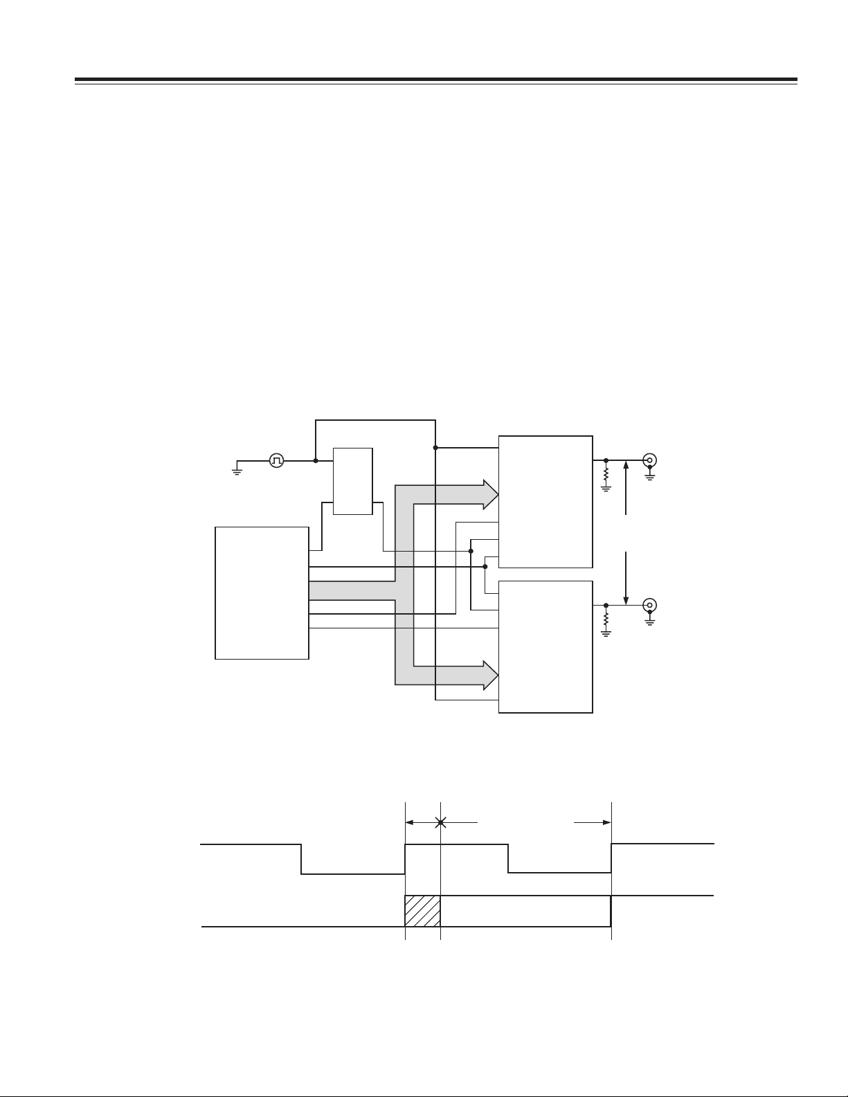
SYNCHRONIZATION INSTRUCTIONS
Figure 3 presents one possible reference design for successful synchronization of multiple DDSs. This example
shows how to place two DDSs into a quadrature phase
relationship.
In Figure 3, the D flip-flop enables the FQ_UD to be synchronous with the REF CLK and provides a setup time
delay. Proper operation may require additional time delay
in the FQ_UD path. This delay depends upon the CK-to-Q
propagation time of the flip-flop. The recommended
timing relationship between the FQ_UD (Pin 8) and the
REF CLK (Pin 9) is depicted in Figure 4.
Here are some general instructions and recommendations
for placing two DDSs into a
quadrature
phase relationship
(refer to Figure 3). There are two sets of instructions, with
and without the 6 REF CLK multiplier enabled.
CK
D FLOP
DQ
FQ_UD
RESET
MICROPROCESSOR
OR FPGA
W_CLK-1
W_CLK-2
8-BIT DATABUS
Instructions for synchronizing two DDSs in quadrature
without the AD9851’s 6 REF CLK multiplier enabled:
1. Power up all devices and apply the common REF CLK.
2. Send a common RESET with a minimum high time of
five REF CLK periods.
3. Program DDS #1 to the desired frequency and a
phase offset of 0 degrees
without
issuing an FQ_UD.
4. Program DDS #2 to the same frequency and a phase
offset of 90 degrees without issuing an FQ_UD.
5. Assert a
common
FQ_UD. This will result in the DAC
outputs becoming active simultaneously at the correct frequency and phase offset as programmed.
6. See Figure 4 for the recommended timing between
REF CLK and FQ_UD.
REF CLK
AD9850/AD9851
#1
DATA
W_CLK
FQ_UD
RESET
RESET
FQ_UD
W_CLK
AD9850/AD9851
#2
DATA
90
PHASE
DIFFERENCE
REV. 0
REF CLK
FQ_UD
REF CLK
Figure 3. Application Circuit
AD9850/AD9851 TIMING RELATIONSHIP
WITHOUT THE 6 REF CLK MULTIPLIER ENABLED
1.5ns
(MIN)
NOT
VALID
THIS TIMING CAN BE TRANSLATED INTO A MINIMUM SETUP
TIME OF 0ns AND A MINIMUM HOLD TIME OF 2 SYSTEM
CLOCK PERIODS.
FQ_UD MUST OCCUR
WITHIN THIS RANGE
VALID
Figure 4. Proper Timing Relationship between REF CLK and FQ_UD
–3–
Page 4
AN-587
CH4
CH1 200mV M 5.00s CH4
2.40V
2.00V
4
1
: 30.0s
@: 29.8s
4
FUD
AD9851 DDS OUTPUT
PLL LOCK TIME
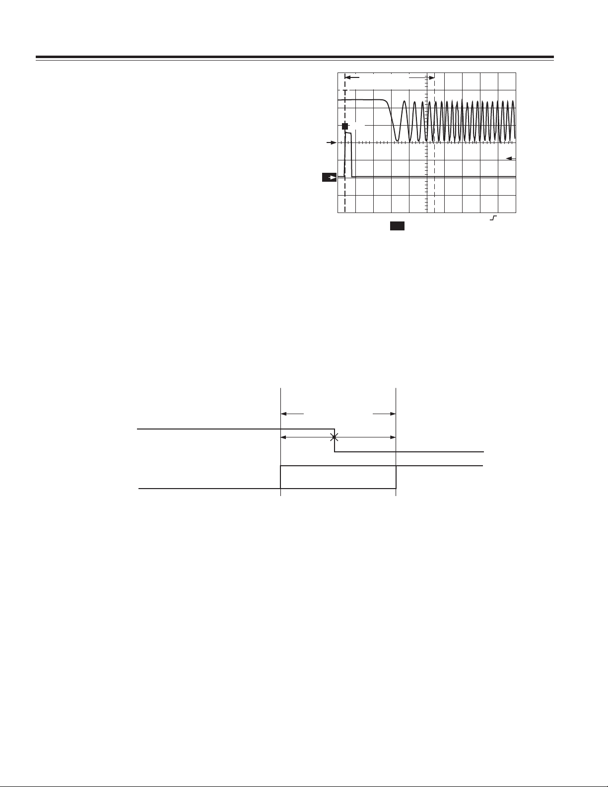
Considerations When Using the 6 REF CLK Multiplier
on the AD9851
The 6 REF CLK multiplier of the AD9851 must be used
with care when synchronizing multiple DDSs because the
PLL lock time will vary from device to device. This means
that the number of system clock cycles delivered to the
phase accumulator at lock time could vary.
This problem is addressed by asserting RESET followed
by programming the tuning word for all devices to zero.
This sets the phase accumulator’s phase to zero and prevents the accumulator from incrementing while the PLL
locks. Once the PLLs lock, all the DDSs are holding at
zero phase. Since all the devices are clocked by a common REF CLK and the PLLs are phase-locked to REF
CLK, all system clock signals will be phase coherent
(assuming a proper REF CLK signal is routed to each
DDS, as previously discussed).
A typical PLL lock time is approximately 30 s. Due to
variations in IC processing and temperature effects on
lock time, it is recommended to allow at least 100 s for
locking to occur (refer to Figure 5).
Figure 5. Typical PLL Lock Time
NOTE: Since the 6 REF CLK multiplier locks to the falling edge of REF CLK, the FQ_UD signal should be
referenced to the falling edge of REF CLK. The recommended timing relationship between the FQ_UD (Pin 8)
and the REF CLK (Pin 9) is depicted in Figure 6.
REF CLK
FQ_UD
AD9851 TIMING RELATIONSHIP
WITH THE 6 REF CLK MULTIPLIER ENABLED
*
FQ_UD MUST OCCUR
WITHIN THIS RANGE
X(ns) Y(ns)
VALID
* FQ_UD SHOULD BE REFERENCED TO THE FALLING EDGE OF REF CLK AND THE
VA LID TIMING RANGE SHALL BE RELATIVE TO A PERCENTAGE OF REF CLK’S PERIOD.
THE VALID TIMING RANGE IS NOT NECESSARILY SYMMETRICAL ABOUT REF CLK’S
FA LLING EDGE. TABLE I DESCRIBES THE “X” AND “Y” SET UP TIME RANGE GIVEN REF
CLK’S FREQUENCY, VCC, AND TEMPERATURE MINIMUM HOLD TIME IS 2 SYSTEM CLK PERIODS.
Figure 6. Proper Timing Relationship Using the 6⫻ Multiplier
–4–
REV. 0
Page 5

AN-587
Instructions for synchronizing two DDSs in quadrature
with the AD9851’s 6 REF CLK multiplier enabled:
1. Power up all devices and apply the common REF CLK.
2. Send a common RESET with a minimum high time of
five REF CLK periods.
3. In parallel or serial mode, write the following instructions to DDS #1
W0 = 01 hex W1 = 00 hex W2 = 00 hex
W3 = 00 hex W4 = 00 hex
4. Repeat step 3 for DDS #2.
5. Assert a
NOTE: This will set each DDS to a tuning word of zero
and engage each REF CLK multiplier simultaneously.
The tuning word of zero will keep the DAC outputs at a
zero phase until the PLLs have finished locking.
IMPORTANT: Remember to keep the REF CLK multiplier
enabled when writing a new tuning word and phase
offset.
6. Program DDS #1 to the desired frequency and a
phase offset of 0 degrees
7. Program DDS #2 to the same frequency and a phase
offset of 90 degrees without issuing an FQ_UD.
common
without
issuing an FQ_UD:
FQ_UD and wait at least 100 ms.
without
issuing an FQ_UD.
Table I. Setup Time Range between FQ_UD
and REF CLK per Frequency, VCC, and Temperature
VCC = 5 V
REF CLK
Frequency
(x) ns (MHz) (y) ns
8 5–7 4
5 7–10 4
3 10–15 3
2 15–20 3
1 20–30 2
VCC = 3.3 V
REF CLK
Frequency
(x) ns (MHz) (y) ns
7 5–7 7
5 7–10 6
2.5 10–15 4
2 15–20 3
Note: Includes Temperature (–40∞C to +85∞ C)
8. Assert a
outputs becoming active simultaneously at the correct frequency and phase offset as programmed.
9. See Figure 6 for the recommended timing between
FQ_UD and REF CLK.
common
FQ_UD. This will result in the DAC
REV. 0
–5–
Page 6
AN-587
CH1
2
CH4
T
T
T
T
100mV M 20.0ns CH4 2.36V
2.00V
1
4
: 96.8s
@: –800ps
DDS2 OUTPUT
DDS1 OUTPUT
CH3 2.00V
3
100mV
18 RISING EDGES
OF THE SYSTEM
CLOCK PLUS THE
SETUP TIME
CH2
30MHz REFERENCE CLOCK
(6-PLL MODE)
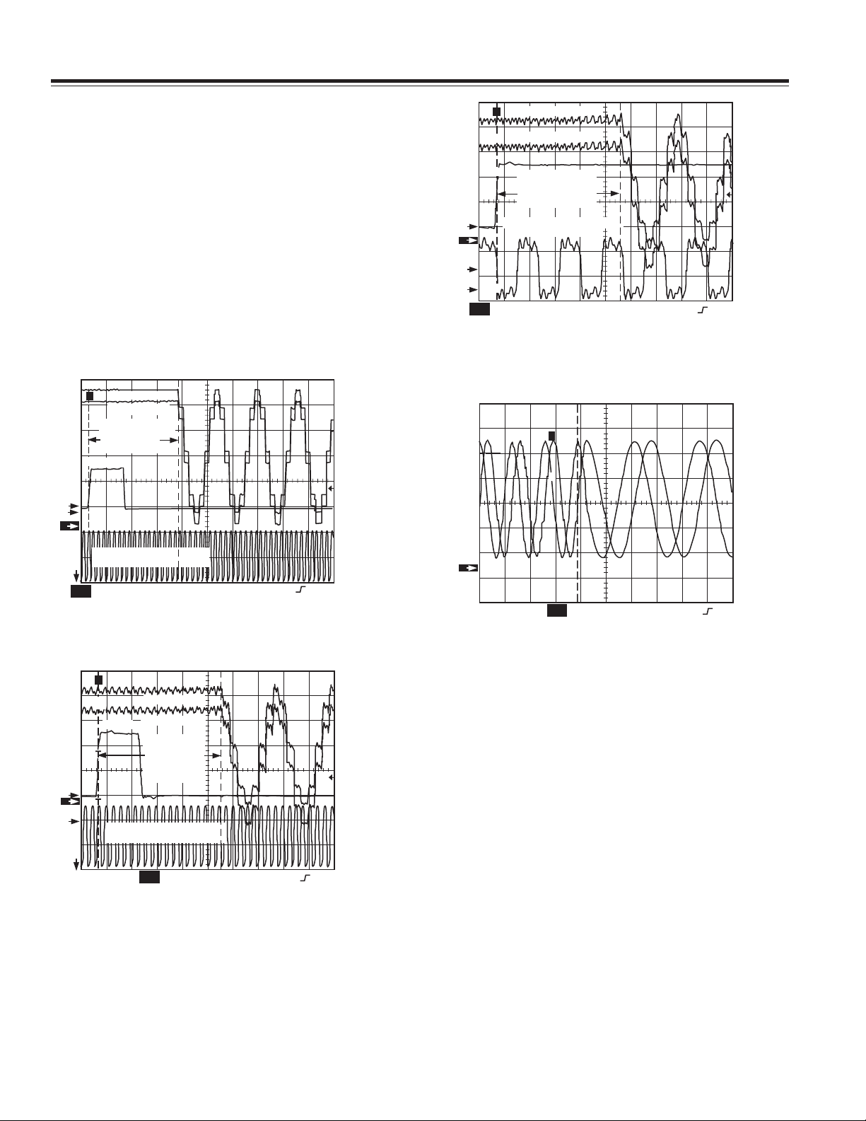
SUMMARY
With proper care and procedure, synchronization can be
achieved among multiple DDSs. The following figures
show how two AD9851s can be synchronized. In
Figure 7, the REF CLK frequency is set to 10 MHz and in
Figure 8, it is set to 180 MHz. Both are in non-PLL
mode. In Figure 9, REF CLK is set to 30 MHz, with PLL
enabled (system clock = 180 MHz). Figure 10 shows two
AD9851s remaining in quadrature, even as the frequency
changes. Quadrature is denoted by the cursor positions on the two signals.
Also shown in Figures 7 through 9 is the fixed pipeline
delay of 18 rising edges of the system clock plus the
setup time. This delay is measured with the cursors
shown in the figures.
T
DDS1 OUTPUT
T
DDS2 OUTPUT
18 RISING EDGES
OF THE SYSTEM
CLOCK PLUS
THE SETUP TIME
T
FQ_UD
: 1.72s
@: 1.69s
Figure 9. DDS Synchronization – Max System CLK
(PLL Mode)
: 1.13s
@: 1.64s
T
T
4
2
1
10MHz REFERENCE CLOCK
3
(NON-PLL MODE)
100mV M 500ns CH4
CH1
CH3 2.00V
CH2
CH4
100mV
2.00V
1.28V
Figure 7. DDS Synchronization – 10 MHz System CLK
T
T
4
2
1
3
CH1
100mV M 20.0ns CH4
CH3 2.00V
Figure 8. DDS Synchronization – Max System CLK
DDS1 OUTPUT
DDS2 OUTPUT
FQ_UD
18 RISING
EDGES OF
THE SYSTEM
CLOCK PLUS
THE SETUP
180MHz REFERENCE CLOCK
(NON-PLL MODE)
100mV
CH2
2.00V
CH4
1.28V
: 96.8s
@: –400ps
2
CH1
100mV M 500ns CH4
CH2
Figure 10. DDS Quadrature Synchronization
2.70V100mV
–6–
REV. 0
Page 7

–7–
Page 8

E02808–0–5/02(0)
–8–
PRINTED IN U.S.A.
 Loading...