

Page 1
AN-581
0.1F
1F
V
S
R2
R1
C1
*STAR GROUND
C
OUT
V
OUT
R
LOAD
VS/2
V
S
/2
R
A
100k
R
B
100k
*
*
V
S
C
IN
V
IN
π ( )
BW1
=
1
2
π 1/2R
ACIN
BW2 =
1
2
π R1 C1
BW3 =
1
2
π R
LOAD COUT
FOR RA = R
B
FOR AC SIGNALS, V
OUT
= VIN (1 + (R2/R1))
WHERE X
C1
<<
R1
*
*
a
APPLICATION NOTE
One Technology Way • P.O. Box 9106 • Norwood, MA 02062-9106 • Tel: 781/329-4700 • Fax: 781/326-8703 • www.analog.com
Biasing and Decoupling Op Amps
in Single Supply Applications
by Charles Kitchin
SINGLE OR DUAL SUPPLY?
Battery-powered op amp applications such as those
found in automotive and marine equipment have only a
single available power source. Other applications, such
as computers, may operate from the ac power lines but
still have only a single polarity power source, such as
5 V or 12 V dc. Therefore, it is often a practical necessity
to power op amp circuits from a single polarity supply.
But single supply operation does have its drawbacks: it
requires additional passive components in each stage
and, if not properly executed, can lead to serious instability problems.
Since a one volt change on the supply line causes a
one-half volt change at the output of the divider, the
circuit’s PSR is only 6 dB. So, the normally high power
supply rejection provided by any modern op amp,
which greatly reduces any ac signals (and power supply hum) from feeding into the op amp via its supply
line, is now gone.
COMMON PROBLEMS WITH RESISTOR BIASING
Single supply applications have inherent problems that
are not usually found in dual supply op amp circuits. The
fundamental problem is that an op amp is a dual supply
device and so some type of biasing, using external components, must be used to center the op amp’s output
voltage at midsupply. This allows the maximum input
and output voltage swing for a given supply voltage.
In some low gain applications, where input signals are
very small, the op amp’s output can be lifted above
ground by only 2 V or 3 V. But in most cases, all clipping
needs to be avoided and so the output needs to be centered around midsupply.
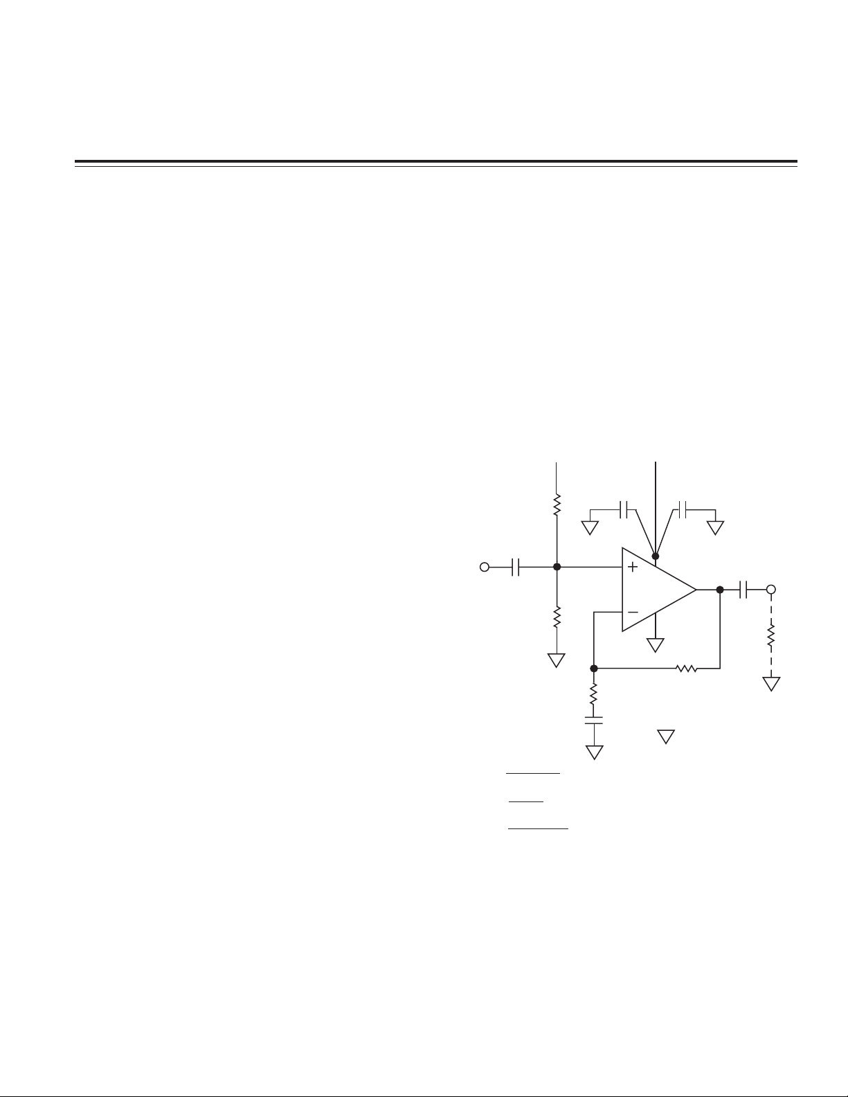
The circuit of Figure 1 shows a simple single supply
biasing method. This noninverting, ac-coupled, amplifier circuit uses a resistor divider with two biasing
resistors, R
ing equal to V
capacitively coupled to the noninverting input terminal.
and RB, to set the voltage on the noninvert-
A
S
/2. As shown, the input signal, VIN, is
This simple circuit has some serious limitations. One is
that the op amp’s power supply rejection is almost entirely
gone, as any change in supply voltage will directly
change the V
Power Supply Rejection (PSR) is a very important (and
frequently overlooked) op amp characteristic.
REV. 0
/2 biasing voltage set by the resistor divider.
S
Figure 1. A Potentially Unstable Single Supply Op
Amp Circuit
© Analog Devices, Inc., 2002
Page 2
AN-581
π
π
π
π
Even worse, instability often occurs in circuits where the
op amp must supply large output currents into a load.
Unless the power supply is well regulated (and well
bypassed), large signal voltages will appear on the supply line. With the op amp’s noninverting input
referenced directly off the supply line, these signals
will be fed directly back into the op amp often initiating
“motor boating” or other forms of instability.
While the use of extremely careful layout, multicapacitor
power supply bypassing, star grounds, and a printed circuit board “power plane,”
may
provide circuit stability,
it is far easier to reintroduce some reasonable amount of
power supply rejection into the design.
DECOUPLING THE BIASING NETWORK FROM THE SUPPLY
The solution is to modify the circuit, as shown in Figure 2.
The tap point on the voltage divider is now bypassed for
ac signals by capacitor C2, restoring some ac PSR.
Resistor R
provides a dc return path for the VS/2 reference
IN
voltage and also sets the circuit’s (ac) input impedance.
V
0.1F
/2
S
1F
R2
150k
*
*STAR GROUND
*
C
OUT
V
S
R
A
100k
R
IN
100k
+
*
BW1 =
BW2 =
BW3 =
BW4 =
FOR RA = RB AND BW1 = 1/10TH BW2,
BW3, AND BW4
FOR AC SIGNALS, V
WHERE X
TO MINIMIZE INPUT BIAS CURRENT ERRORS,
R2 SHOULD EQUAL R
Figure 2. A Decoupled Single Supply Op Amp Biasing
Circuit
C2
V
2
2
2
2
IN
(1/2RA) C2
1
RIN C
1
R1 C1
R
LOAD COUT
<<R1
C1
1
1
R
B
100k
IN
C
IN
= VIN (1 + (R2/R1))
OUT
(1/2 R
+
IN
*
V
S
VS/2
R1
C1
*
)
A
Many published applications circuits show a 100 kΩ/100 kΩ
voltage divider for R
and RB with a 0.1 µF or similar
A
capacitance value for C2. However, the –3 dB bandwidth
of this network is set by the parallel combination of R
A
and RB and Capacitor C2 and is equal to:
–
3
dB BW
(, )(. )
250000 0 1 10
π
1
–
6
Farads
×
30
Hz=
=
Motor boating or other forms of instability can still occur,
as the circuit has essentially no power supply rejection
for frequencies below 30 Hz. So any signals below 30 Hz
that are present on the supply line, can very easily find
their way back to the + input of the op amp.
A practical solution to this problem is to increase the
value of capacitor C2. It needs to be large enough to
effectively bypass the voltage divider at all frequencies
within the circuit’s passband. A good rule of thumb is to
set this pole at one-tenth the –3 dB input bandwidth, set
by R
IN/CIN
and R1/C1.
Note that the dc circuit gain is unity. Even so, the op
amp’s input bias currents need to be considered. The
R
voltage divider adds considerable resistance in
A/RB
series with the op amp’s positive input terminal, equal
to the parallel combination of the two resistors. Maintaining the op amp’s output close to midsupply requires
“balancing” this resistance by increasing the resistance
in the minus input terminal by an equal amount. Current
V
OUT
R
AD
LO
feedback op amps often have unequal input bias currents, which further complicates the design.
Therefore, designing a single supply op amp circuit
design that considers input bias current errors as well as
power supply rejection, gain, input and output circuit
bandwidth, etc., can become quite involved. However, the
design can be greatly simplified by using a “cookbook”
approach. For a common voltage feedback op amp
operating from a 15 V or 12 V single supply, a resistor
divider using two 100 kΩ resistors is a reasonable compromise between supply current consumption and input
bias current errors. For a 5 V supply, the resistors can be
reduced to a lower value such as 42 kΩ. Finally, some
applications need to operate from the new 3.3 V standard. For 3.3 V applications, it is essential that the op
amp be a “rail-to-rail” device and be biased very close to
midsupply; the biasing resistors can be further reduced
to a value of around 27 kΩ.
–2–
REV. 0
Page 3
AN-581
π (
π
Note that current feedback op amps are typically
designed for high frequency use and a low-pass filter is
formed by R2 and stray circuit capacitance, which can
severely reduce the circuit’s 3 dB bandwidth. Therefore,
current feedback op amps normally need to use a
fairly low resistance value for R2. An op amp such as
the AD811, which was designed for video speed applications, typically will have optimum performance using a
1kW resistor for R2. Therefore, these types of applications
need to use much smaller resistor values in the R
A/RB
voltage divider to minimize input bias current errors.
Instead of a bipolar device, the use of a modern FET
input op amp will greatly reduce any input bias current
errors unless the circuit is required to operate over a
very wide temperature range. In that case, balancing the
resistance in the op amp’s input terminals is still a wise
precaution.
Table I provides typical component values for the circuit
of Figure 2 for several different gains and 3 dB bandwidths.
Table I. Typical Component Values for the Circuit of Figure 2
Where R
= RB = 100 k⍀, RIN = 100 k⍀, and R2 = 150 k⍀
A
Input Output
BW BW C
*R1 C1* C2 C
IN
OUTRLOAD
Gain (Hz) (Hz) (F) (k⍀)(F) (F) (F) (k⍀)
10 10 10 0.3 16.5 1.5 3 0.2 100
20 10 10 0.3 7.87 3 3 0.2 100
10 50 50 0.1 16.5 0.3 0.6 0.05 100
101 20 20 0.2 1.5 6.8 2 0.1 100
*Capacitance values rounded off to next highest common value. Since
the CIN/RIN pole and C1/R1 poles are at the same frequency, and both
affect the input BW, each capacitor is ÷2 larger than it would otherwise
be for a single pole RC-coupled input. C2 is selected to provide a corner
frequency of 1/10th that of the input BW.
+V
S
0.1F
R
A
100k⍀
R
2
2
2π R
R1 C1
B
100k⍀
V
IN
1
1/2 RA) C2
1
1
LOAD COUT
OUT
C2
*
BW1 =
BW2 =
BW3 =
FOR RA = RB AND XC2<<X
FOR AC SIGNALS, V
WHERE XC1<<R1
TO MINIMIZE INPUT BIAS CURRENT ERRORS,
R2
SHOULD EQUAL 1/2 R
*
VS/2
VS/2
R1
C1
= VIN (R2/R1)
.
A
C1
+V
S
1F
R2
*
50k⍀
*STAR GROUND
*
C
OUT
V
OUT
R
LOAD
Figure 3. A Decoupled Single Supply Inverting
Amplifier Circuit
Figure 3 shows a circuit similar to Figure 2, but for an
inverting amplifier.
Table II provides typical component values for several
different gains and 3 dB bandwidths.
Table II. Typical Component Values for the Circuit of Figure 3
Where R2 = 50 k⍀ and R
= RB = 100 k⍀
A
Input Output
BW BW R1 C1* C2* C
OUTRLOAD
Gain (Hz) (Hz) (k⍀)(F) (F) (F) (k⍀)
10 10 10 2 8.2 0.5 0.2 100
20 10 10 1 20 0.5 0.2 100
10 50 50 2 2 0.1 0.05 100
100 20 20 1 8.2 0.3 0.1 100
*Capacitance values rounded off to next highest common value. Since
the C1/R1 pole and C2/RA/RB poles are at the same frequency, and both
affect the input BW, each capacitor is ÷2 larger than it would otherwise
be for a single pole RC-coupled input.
REV. 0
–3–
Page 4

AN-581
π
π
π
ZENER DIODE BIASING
Although the resistor divider biasing technique is low
cost, and always keeps the op amp’s output voltage at
V
/2, the op amp’s common-mode rejection is entirely
S
dependent upon the R
time constant formed by RA/R
C
and capacitor C2. Using a C2 value that provides at least
10 times the R
network (R1/C1 and R
time constant of the input RC coupling
C
) will help ensure a reasonable
IN/CIN
common-mode rejection ratio. With 100 kΩ resistors for
R
and RB, practical values of C2 can be kept fairly small
A
as long as the circuit bandwidth is not too low. However,
another way to provide the necessary V
/2 biasing for
S
single supply operation is to use a Zener diode regulator.
Just such a scheme is shown in Figure 4. Here, current
flows through resistor R
to the Zener. Capacitor C
Z
helps prevent any Zener-generated noise from feeding
into the op amp. Low noise circuits may need to use a
larger value for C
V
IN
I
Z
V
S
R
Z
than the 10 µF specified.
N
V
S
0.1F
C
IN
R
IN
100k
+
C
10F
*
V
Z
V
Z
N
*
1F
V
100k
*
C
OUT
V
Z
Z
R2
V
R
OUT
LOAD
A Zener should be chosen that has an operating voltage
close to V
/2. Resistor RZ needs to be selected to provide
S
a high enough Zener current to operate the Zener at its
stable rated voltage and to keep the Zener output noise
B
low. It is also important to minimize power consumption
(and heating) and to prolong the life of the Zener. As the
op amp’s input current is essentially zero, it’s a good
idea to choose a low power Zener. A 250 mW device is best
but the more common 500 mW types are also acceptable.
The ideal Zener current varies with each manufacturer
but practical I
levels between 5 mA (250 mW Zener) and
Z
5 µA (500 mW Zener) are usually a good compromise for
this application.
N
Within the operating limits of the Zener, the circuit of
Figure 4 basically restores the op amp’s power supply
rejection. But this does not come without a price: the op
amp’s output is now at the Zener voltage rather than at
V
/2. If the power supply voltage drops, nonsymmetrical
S
clipping can occur on large signals. Furthermore, the circuit now consumes more power. Finally, input bias
currents still need to be considered. Resistors R
and R2
IN
should be close to the same value to prevent input bias
currents from creating a large offset voltage error.
Figure 5 is an inverting amplifier circuit using the same
Zener biasing method.
R1
C1
*STAR GROUND
SELECT RZ TO PROVIDE THE DESIRED
ZENER OPERATING CURRENT, I
+V
– V
S
ZENER
=
R
Z
I
Z
1
BW1 =
2
RIN C
IN
1
BW2 =
2
R1 C1
2
1
R
LOAD COUT
OUT
BW3 =
FOR AC SIGNALS, V
WHERE XC1<<R1
TO MINIMIZE INPUT BIAS CURRENT ERRORS,
R2 SHOULD EQUAL RIN.
SEE TEXT.
.
Z
= VIN (1 + (R2/R1))
*
Figure 4. A Noninverting Single Supply Amplifier Using
Zener Diode Biasing
–4–
REV. 0
Page 5

π
π
π
V
S
0.1F
R
I
Z
V
S
R
Z
ZENER
IN
100k
10 F
C2
*
V
Z
V
Z
+
*
V
IN
R1
C1
*
1F
R2
100k
*
C
OUT
V
Z
R
*STAR GROUND
SELECT RZ TO PROVIDE THE DESIRED
ZENER OPERATING CURRENT, I
– V
+V
S
ZENER
=
R
Z
I
Z
2
2
2
R1 C1
RIN C2
R
1
1
1
LOAD COUT
OUT
IN
BW1 =
BW2 =
BW3 =
FOR AC SIGNALS, V
WHERE XC1<<R1
TO MINIMIZE INPUT BIAS CURRENT ERRORS,
R2 SHOULD EQUAL R
.
Z
= VIN (R2/R1)
.
SEE TEXT.
Figure 5. An Inverting Single Supply Amplifier Using
Zener Diode Biasing
V
OUT
LOAD
AN-581
Table III can be used with circuits 4 and 5 to provide
practical R
Zener diodes. Note that for the lowest possible circuit
noise, the optimum Zener current should be selected by
referring to the Zener product data sheet.
Table III. Recommended RZ Values and Motorola Zener
Diode Part Numbers for Use with Figures 4 and 5
Supply Zener Zener R
Voltage Voltage Zener Current Value
(V) (V) Type (IZ)()
+15 7.5 1N4100 500 µA 15 k
+15 7.5 1N4693 5 mA 1.5 k
+12 6.2 1N4627 500 µA 11.5 k
+12 6.2 1N4691 5 mA 1.15 k
+9 4.3 1N4623 500 µA 9.31 k
+9 4.3 1N4687 5 mA 931
+5 2.4 1N4617 500 µA 5.23 k
+5 2.7 1N4682 5 mA 464
Tables IV and V provide practical component values
for Figures 4 and 5 for several different circuit gains
and bandwidths.
Table IV. Typical Component Values for the Circuit of
Figure 4 Where R
from Table III
Gain (Hz) (Hz) (F) (k)(F) (F) (k)
10 10 10 0.3 11.0 2 0.2 100
20 10 10 0.3 5.23 4.7 0.2 100
10 50 50 0.1 11.0 0.47 0.05 100
101 20 20 0.2 1.0 15 0.1 100
*Capacitance values rounded off to next highest common value. Since
the CIN/RIN pole and C1/R1 poles are at the same frequency, and both
affect the input BW, each capacitor is √2 larger than it would otherwise
be for a single pole RC-coupled input.
resistor values for use with some common
Z
= R2 = 100 k and CN = 0.1 F. Select R
IN
Input Output
BW BW C
*R1 C1* C
IN
Z
Z
OUTRLOAD
Table V. Typical Component Values for the Circuit of
Figure 5 Where R
= R2 = 100 k. Select RZ from Table III
IN
Input Output
BW BW R1 C1* C2* C
OUTRLOAD
Gain (Hz) (Hz) (k)(F) (F) (F) (k)
10 10 10 10 2.7 0.2 0.2 100
20 10 10 5 4.7 0.2 0.2 100
10 50 50 10 0.5 0.05 0.05 100
100 20 20 1 12 0.1 0.1 100
*Capacitance values rounded off to next highest common value. Since
the C1/R1 pole and C2/RIN poles are at the same frequency, and both
affect the input BW, each capacitor is √2 larger than it would otherwise
be for a single pole RC-coupled input.
REV. 0
–5–
Page 6

AN-581
0.1F
1F
*
*
*STAR GROUND
VS/2
+V
S
–V
S
VS/2
*
*
R
A
220k
C2
0.1F
R
B
220k
+
110k
0.1
F
1F
*
0.1F
OP AMP BIASING USING A LINEAR VOLTAGE REGULATOR
For op amp circuits operating from the new 3.3 V standard,
a 1.65 V biasing voltage is needed. Zener diodes are
commonly available only down to 2.4 V. The easiest way
to provide this biasing voltage is to use a linear voltage
regulator, such as the ADM663A or ADM666A devices.
This is shown in Figure 6.
V
S
V
IN
SENSE
V
(2)
GND
OUT
V
SET
1.3V T O 16V
ADJUSTABLE
OUTPUT
V
IN
REF
C1
R
A
R
B
*
R1
ADM663A
ADM666A
Figure 6. An Op Amp Single Supply Biasing Circuit Using
A Linear Voltage Regulator
Although a Zener diode is usually the cheapest voltage
regulator available, a linear voltage regulator has lower
drift over temperature than a Zener and far less noise.
Resistors R
V
/2 voltage reference; consult AD663A datasheet.
S
and RB are selected to provide the desired
A
DC-COUPLED BATTERY-POWERED CIRCUITS
So far, only ac-coupled op amp circuits have been
discussed. Although with the use of suitably large input
and output coupling capacitors, an ac-coupled circuit can
operate at frequencies well below 1 Hz, some applications
require a true dc response.
Battery-powered applications permit the use of a “phantom ground” circuit as shown in Figure 7. This provides
dual supply voltages, both positive and negative with respect to ground, from a single battery. An op amp is
used to buffer the output of a V
low voltage battery such as 3.3 V is used, the op amp
should be a “rail-to-rail” device and able to operate
effectively from this supply voltage. The op amp also
needs to be able to supply an output current large
enough to power the load circuit. Capacitor C2 bypasses
the voltage divider output enough to prevent any resistor
noise from feeding into the op amp. This capacitor does
not need to provide power supply rejection because the
load current flows directly to ground and so any signal
currents flow equally from both sides of the battery.
Resistors R
V
S
and RB are selected to provide the desired
A
/2 voltage reference; consult AD663A datasheet.
V
S
0.1F1F
*
VS/2
/2
V
S
/2 voltage divider. If a
S
*
*
R2
*STAR GROUND
C
OUT
V
OUT
R
LOAD
Figure 7. Using an Op Amp to Provide a “Phantom
Ground” for Battery-Powered DC-Coupled Applications
NOISE ISSUES
Some op amp applications need a low noise amplifier
and low noise amplifier circuits require low resistance
values in the signal path. Johnson (resistor) noise
equals 4 nV times the square root of the resistance
value in kΩ. While the Johnson noise of a 1 kΩ resistor
is only 4 nV/√Hz, this increases to 18 nV/√Hz for a 20 kΩ
resistor and 40 nV/√Hz for a 100 kΩ resistor. Even though
the R
resistor divider is bypassed to ground with a
A/RB
capacitor (C2), these resistors set a limit on the minimum value that can be used for the op amp’s feedback
resistor and, the larger this is, the greater the Johnson
noise. So low noise applications need to use much
smaller op amp biasing resistor values than the 100 kΩ
specified here. However, lower value resistors in the
divider mean higher power supply current and reduced
battery life.
Fortunately, the Zener diode biasing method supplies
V
/2 without the need for large resistors. As long as the
S
Zener is bypassed to keep its noise out of the circuit,
both noise and supply current can be kept low. The use
of a linear voltage regulator is even better, as its noise
and output impedance are both very low.
–6–
REV. 0
Page 7
AN-581
CIRCUIT TURN-ON TIME ISSUES
One final issue that needs to be considered is circuit
turn-on time. The approximate turn-on time will equal
the R
time constant of the lowest BW filter being used.
C
The circuits shown here all call for the RA/RB, C2 voltage
divider network to have a 10 times longer time constant
than that of the input or output circuit. This is to simplify
the circuit design (since up to three different R
poles set
C
the input BW). This long time constant also helps keep
the biasing network from “turning on” before the op
amp’s input and output networks and, therefore, the op
amp’s output gradually climbs from zero volts to V
/2
S
without “railing” to the positive supply line. The value
supplied by this table is for a 3 dB corner frequency that
is 1/10th that of R1/C1 and R
LOAD/COUT
. For example: in
Figure 2, for a circuit BW of 10 Hz and a gain of 10, Table
I recommends a C2 value of 3 µF, which provides a 3 dB
bandwidth of 1 Hz.
Fifty thousand ohms (the parallel combination of R
R
) times 3 microFarads equals an RC time constant of 0.15
B
and
A
seconds. So the op amp’s output will take 0.15 seconds
(approximately) to settle to V
/2. The input and output R
S
networks will charge up ten times faster.
In some applications, where the circuit’s –3 dB low
frequency bandwidth is very low, the circuit turn-on
time may become excessively long. In that case, a
Zener biasing method may be a better choice.
INPUT “HEADROOM” CONSIDERATIONS
Some specialty op amps are designed for low voltage
operation. When these are operated from a low voltage,
single supply, such as 5 V or 3.3 V, input headroom limitations may be introduced. This can happen if the
amplifier’s input stage does not limit symmetrically.
For example: the AD8061 op amp is designed to have an
input common-mode voltage range that extends all the
way down to “ground” (or the negative supply line).
However, its inputs can only swing to within 1.8 V of the
positive supply voltage without introducing dc errors or
limiting device bandwidth. So, if this amplifier is operated from a single 5V supply and the amplifier’s positive
input is biased at V
/2 (2.5 V), the input voltage can
S
swing in the negative direction a full 2.5 V (down to zero
volts). But, in the positive direction, it can only swing 1 V
before clipping.
Note that this is not a problem if the amplifier is being
operated at a gain of 2.5 or higher, as the maximum output swing (± 2.5 V) will be reached before the input stage
limits. However, if the amplifier is being operated at a
C
lower gain, the positive input needs to be biased below
V
/2, to allow symmetrical input stage limiting. In the
S
case of the AD8061, biasing the positive input at 1.5 V
will allow a 3 V p-p input swing without clipping. Refer
to the individual product data sheet to determine the
optimum single supply biasing voltage.
Table VI. Rail-to-Rail Op Amps Recommended for New Designs
Type Single Dual Quad
High Speed AD8031 AD8032
AD8061 AD8062
AD8051 AD8052 AD8054
AD8063 AD823
High Output AD8591 AD8592 AD8594
AD8531 AD8532 AD8534
JFET Input AD820 AD822 AD824
Auto Zero AD8551 AD8552 AD8554
Digital Trim AD8601 AD8602 AD8604
Low Noise OP184 OP284 OP484
OP162 OP262 OP462
AD8605 AD8606 AD8608
AD8628
Low Power OP196 OP296 OP496
AD8541 AD8542 AD8544
Precision OP777 OP727 OP747
REV. 0
–7–
Page 8

E02493–0–10/02(0)
–8–
PRINTED IN U.S.A.
 Loading...