


9106
www.analog.com
Etienne Moulin
ADE7756 (i.e., AN-564 reference design) and, in addition
to the active energy measurement, provides the voltage
ADE7756 with a microcontroller. The communication
through a serial interface (SPI). The SPI port allows
the user to calibrate various components of the meter
to store various calibration parameters of the meter and
to store the meter’s data during a power-down.
tion of active energy. Circuitry is provided to null out
various system errors including gain, phase, and offset
All registers of the ADE7756 are available through the
to process rms calculation into the microcontroller. This
the meter.
14 of program memory, and a 4 kbytes
this document is to demonstrate that a cost-effective
voltage input.
further details on the accuracy achievements of this refer-

–2
–
THEORY OF CALCULATION
V
T
V t
dt
RMS
0
T
= ×
( )
∫
1
2
the square root
V
N
V i
RMS
i
N
= ×
∑
=
1
2
1
( )
factor to the mean absolute value
V
2
V
RMS MAV
=
×
×
π
2
tive Power and the Apparent Power consumed by a load.
PF
Active Power
Apparent Power
=
Active Power (t) Mean V(t) I(t)
Apparent Power V I
RMS RMS
= ×
( )
= ×
is the phase difference between the volt-
the reactive energy. When the active power and the real
Reactive Power Apparent Power Active Power
2 2
= −
Averaging
the more samples used for rms calculation, the more
the measurement depends on both measurement time
variation of these parameters in terms of dynamic range
the averaging time needed for an accurate rms measure-
Amplitude Dynamic Range:
Voltage 10:1
Period of Change of the Amplitude: 3 Seconds
Frequency of the Signal:
Windowing Effect
A commonly used method for canceling the windowing
–3
–
+ V
t) yields:
V
/2 + 2
V
V
cos (
t) + V
/2
cos (2
t)
DC COMPONENT (INCLUDING ERROR TERM) IS EXTRACTED
BY THE LPF FOR REAL POWER CALCULATION
FREQUENCY – rad/s
0 2
V
2
OS
V
2
2
V
2
2
2 V
OS
V
and 2
the rms calculation.
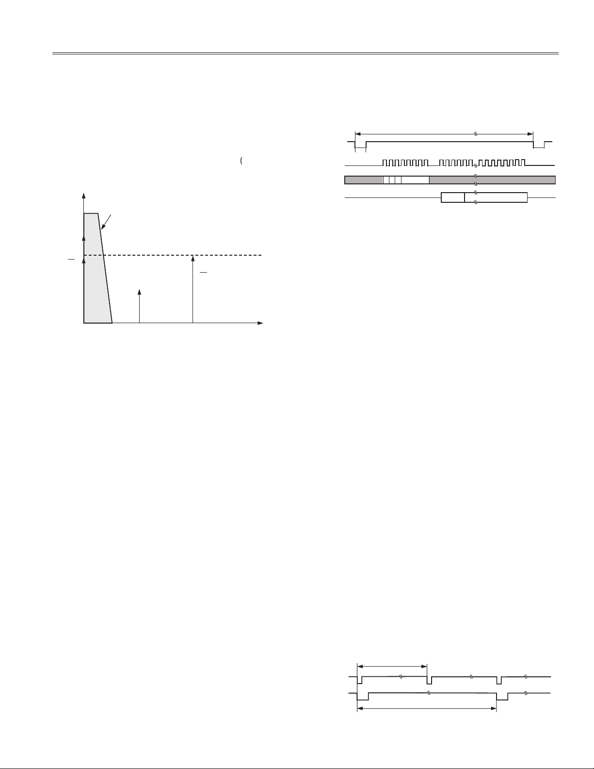
ADE7756 Sampling Mode
through a special mode called waveform sampling
ADE7756 data sheet). The sampling rate of the output
four ch o i c e s : CLKI N / 1 2 8 , CL K I N / 2 5 6 , CLKIN / 5 1 2 ,
IRQ
pin low for 16 µs
when a new sample is available in the waveform reg-
When the sampling period is over, another interrupt
0 0 0 01 HEX
SAMPLING RATE (CLKIN/128, CLKIN/256, CLKIN/512, OR CLKIN/1024)
IRQ
SCLK
DIN
DOUT
READ FROM WAVEFORM
CHANNEL 1 OR CHANNEL 2 DATA – 20 BITS
16s
SIGN
As discussed later, the rms computation implemented in
worst-case computation time of approximately 350 µs.
ADE7756 can be sped up to 5 MHz (see the ADE7756 data
ADE7756.
time needed for the microcontroller to process the data
through the required rms signal processing determines
the sampling frequency of the input.
With this frequency, the sampling periods available
through the ADE7756 are 35.7 µs, 71.5 µs, 143 µs, and
the signal processing, the lowest sampling rate is used
for the ADE7756 and the samples are read with a decima-
tion factor of 2. The actual sampling rate for the samples
which represents approximately 1.748 kHz.
SAMPLING RATE (CLKIN/1024)
IRQ
CS
READING RATE = CLKIN/2048

–4
–
the rms calculation signal processing. Depending on the
tered to extract the dc component (see Figure 1). After the
tion and conversion to true rms information is then
very important because it reduces the computation time
Averaging/Low-Pass Filter
Averaging the output of the squared input can be done by
ltering solution is implemented in the microcontroller
with a rst order in nite impulse response lter (IIR l-
ter). The architecture of this lter is shown in Figure 5; the
lter reduces the number of mathematical operations
gain parameters and by limiting the
is done, the
2
–P
X
N
2N 2N+P
2
P
+
–
+
2N
Y
N
Z
–1
+
Y
X
2
1 (1+ 2 )
Z
N
N
P
P 1
=
−
−
− −
where 2
is the operand of the IIR lter.
F
2
2
f
C
P
SAMPLING
= ×
−
π
–P
is the actual operand of
the lter.
Σ
VOLTAGE OR
CURRENT
INPUT
UPPER MSB
LPF
OFFSET GAIN
RMS
20
19 12
OR
17
X

–5
–
10
100 1000
1.000.100.01
–40
0
FREQUENCY – Hz
–20
–60
–70
H – dB
–10
–30
–50
–45dB ATTENUATION
@ 100Hz
–3dB CUTOFF
FREQUENCY = 0.55Hz
frequency can be lowered but then it takes more samples
2500
4500 5500
1500500–500
SAMPLES
3500
ERROR 0.1%
1.2
1.0
0.8
0.6
0.4
0.2
0.0
At the given sampling frequency, 3,540 samples repre-
Errorn(%) =
+
( )
×
−
1
1 2
100
9
where
represents the number of samples.
When the output of the low-pass lter has settled,
the square of the rms value of the input signal can be
value of the selected input on an LCD display.
Various algorithms exist to process the square root. A
the output and the output, depending on the result of the
value of the low-pass lter is a 20-bit register; the square
X
2
SAR
X
N
2N
Y
N
N
+
–
An offset compensation is introduced to eliminate the
the LCD after a binary-to-decimal conversion.
voltage channel speci cs.
After the offset and gain compensation, the rms result
the digital signal processing to the format of the display.

–6
–
An interrupt servicing routine takes care of all the timers’
threshold (SAG detection). The microcontroller services
the interrupts (internal and external) as described in the
AN-564 reference design.
ADE7756. When an interrupt occurs, the microcontroller
tion (SAG pin = low) or a waveform sample available
ADE7756’s register. This functionality is very important to
tion mode. The power-down mode is described in more
RMS
CALCULATION MODE
ENABLE WFSM
AND SAG INTERRUPTS
REAL-TIME
RMS ROUTINE
DISABLE WFSM
INTERRUPT
POST-PROCESSING
RMS ROUTINE
NORMAL MODE
SAG PIN = HIGH
END OF
REAL-TIME RMS
ROUTINE?
INTERRUPT
INTERRUPT
INTERRUPT
NO
NO
NO
YES
YES
YES
ENERGY DUMP
ROUTINE
INITIALIZATION
tronics energy meter.
the ADE7756 is used not only for energy accumulation,
to maintain the performance and behavior of the
AN-564 reference design.
When the ADE7756 is used in waveform sampling mode,
the active energy register cannot be read at the same
time. Nevertheless, the active energy is still accumulated
full-scale ac energy (see the ADE7756 data sheet). As the
NORMAL MODE
READ
ACTIVE ENERGY
REGISTER
STORE CONSUMED
ENERGY
IN EEPROM
CONFIGURATION OF
THE ADE7756
FOR RMS CALCULATION
RMS CALCULATION
READ
ACTIVE ENERGY
REGISTER
STORE CONSUMED
ENERGY IN EEPROM
CONFIGURATION OF
THE ADE7756
FOR NORMAL MODE
RMS
CALCULATION?
RMS VALUE
NO
YES

–7
–
the rms information is not needed every three seconds,
the corner frequency of the low-pass lter can be changed
to reduce the effect of the ripple frequency. The drawback
the rms information.
to deliver this information. There are no additional rm-
ware routines necessary to process this information as
PercentageError
True RMS RMS Measurement
True RMS
100%=
−
×
tor, compared to 7 mA when the meter is in an energy
1000
1000.1
1.00%
VOLTAGE – V
MAX % ERROR
0.90%
0.80%
0.70%
0.60%
0.50%
0.40%
0.30%
0.20%
0.10%
0.00%
100
10.1
1.00%
CURRENT – A
MAX % ERROR
10
0.90%
0.80%
0.70%
0.60%
0.50%
0.40%
0.30%
0.20%
0.10%
0.00%

–8
–
tered trademarks are the property of their respective companies.
 Loading...