AN-577
DCLK
GND
+V
CC
BUSY
PENIRQ
PEN
INTERRUPT
SAR + ADC
CONTROL LOGIC
SPORT
CS
DOUTDIN
6-TO-1
I/P
MUX
AD7873
+V
CC
AUX
V
REF
Y–
Y+
X–
X+
V
BAT
TEMP
SENSOR
CHARGE
REDISTRIBUTION
DAC
2.5V
REF
BUF
BATTERY
MONITOR
T/H
COMP
a
APPLICATION NOTE
One Technology Way • P.O. Box 9106 • Norwood, MA 02062-9106 • 781/329-4700 • www.analog.com
Layout and Grounding Recommendations for Touch Screen Digitizers
by Nicola O’Byrne
INTRODUCTION
This application note provides layout suggestions to optimize the performance of the AD7843/AD7873. The
AD7843/AD7873 are 12-bit successive-approximation
ADCs with a synchronous serial interface and low onresistance switches for driving touch screens. The
AD7843/AD7873 operate from a single 2.2 V to 5.25 V
power supply and feature throughput rates greater
than 125 kSPS.
GROUNDING AND LAYOUT
Both supplies to each of the AD7843 and AD7873 are
analog supplies and should be connected directly
together. Although various portable applications may
have conflicting requirements with respect to power
consumption, cost, size or weight, most should have
relatively clean power supplies and ground as the power
supply is from a battery and most of the internal components are very low power. However care should still be
taken with regard to grounding and layout. It should
also be noted that each situation is unique and the following suggestions should be carefully reviewed.
The printed circuit board that houses the AD7843 or the
AD7873 should be designed so the analog and digital
sections are separated and confined to certain areas of
the board. This facilitates the use of ground planes that
can easily be separated. A minimum etch technique is
generally best for ground planes as it gives the best
shielding. The GND pin of the AD7843/AD7873 should
be sunk in the analog ground plane. The AGND plane
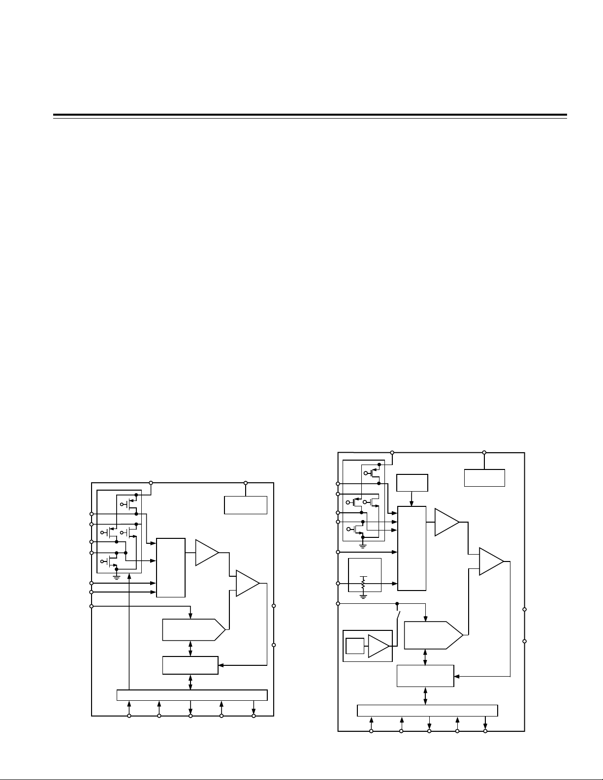
FUNCTIONAL BLOCK DIAGRAMS
+V
CC
AD7843
4-TO-1
I/P
MUX
CHARGE
REDISTRIBUTION
SAR + ADC
CONTROL LOGIC
CS
T/H
DAC
SPORT
DOUTDIN
X+
X–
Y+
Y–
IN3
IN4
V
REF
DCLK
PENIRQ
PEN
INTERRUPT
COMP
BUSY
GND
+V
CC
REV. 0
© Analog Devices, Inc., 2001

AN-577
and DGND plane connection should be made at one
point only, a star ground point that should be established as close as possible to the GND pin of the
AD7843/AD7873.
Avoid running digital lines under the device as these will
couple noise onto the die. The analog ground plane
should be allowed to run under the AD7843/AD7873 to
avoid noise coupling. The power supply lines to the
AD7843/AD7873 should use as large a trace as possible
to provide low impedance paths and reduce the effects
of glitches on the power supply line. Fast switching signals like clocks should be shielded with digital ground to
avoid radiating noise to other sections of the board, and
clock signals should never be run near the analog
inputs. Care should be taken to restrict digital signals
from overshoot or undershoot, even on a transient basis. Avoid crossover of digital and analog signals.
Traces on opposite sides of the board should run at right
angles to each other. This will reduce the effects of
feedthrough through the board. A microstrip technique
is by far the best but is not always possible with a
double-sided board. In this technique, the component
side of the board is dedicated to ground planes while
signals are placed on the solder side.
Good decoupling is also important. All analog supplies
should be decoupled with 10 µF tantalum in parallel with
0.1 µF capacitors to AGND. To achieve the best from
these decoupling components, they must be placed as
close as possible to the device, ideally right up against
the device.
The AD7843/AD7873 architecture offers no inherent rejection of noise or voltage variation with respect to the
use of an external reference. This is of particular concern if the reference input is tied to the power supply.
Any noise or ripple on the supply will appear directly in
the digital output. Although high-frequency noise can be
filtered out, voltage variation due to line frequency
(50 Hz or 60 Hz) can be difficult to remove.
Digitizer to Touch Screen Interconnection
In the specific case of use with a resistive touch screen,
care should be taken with the connection between the
converter and the touch screen. Since resistive touch
screens can have quite low resistance, the interconnection should be as short and robust as possible. Longer
connections will act as a source of error much like the
on-resistance of the internal switches which can be
negated using the differential reference architecture of
the devices. Similarly, loose connections can be a
source of error when the contact resistance changes
with flexing or vibrations. Noise can be a major source
of error in touch screen applications (e.g., applications
that require a back-lit LCD panel). This EMI noise can be
coupled through the LCD panel to the touch screen and
cause “flickering” of the converted data. Several things
can be done to reduce this error, such as utilizing a
touch screen with a bottom-side metal layer connected
to ground. This will couple the majority of noise to
ground. Additionally, filtering capacitors from Y+, Y–,
X+, and X– to ground, can also help. Caution should be
observed for settling time of the touch screen, especially
when operating the AD7843/AD7873 in the single ended
mode and at high data rates. See the AD7843 and
AD7873 data sheets for more detailed information on
settling time.
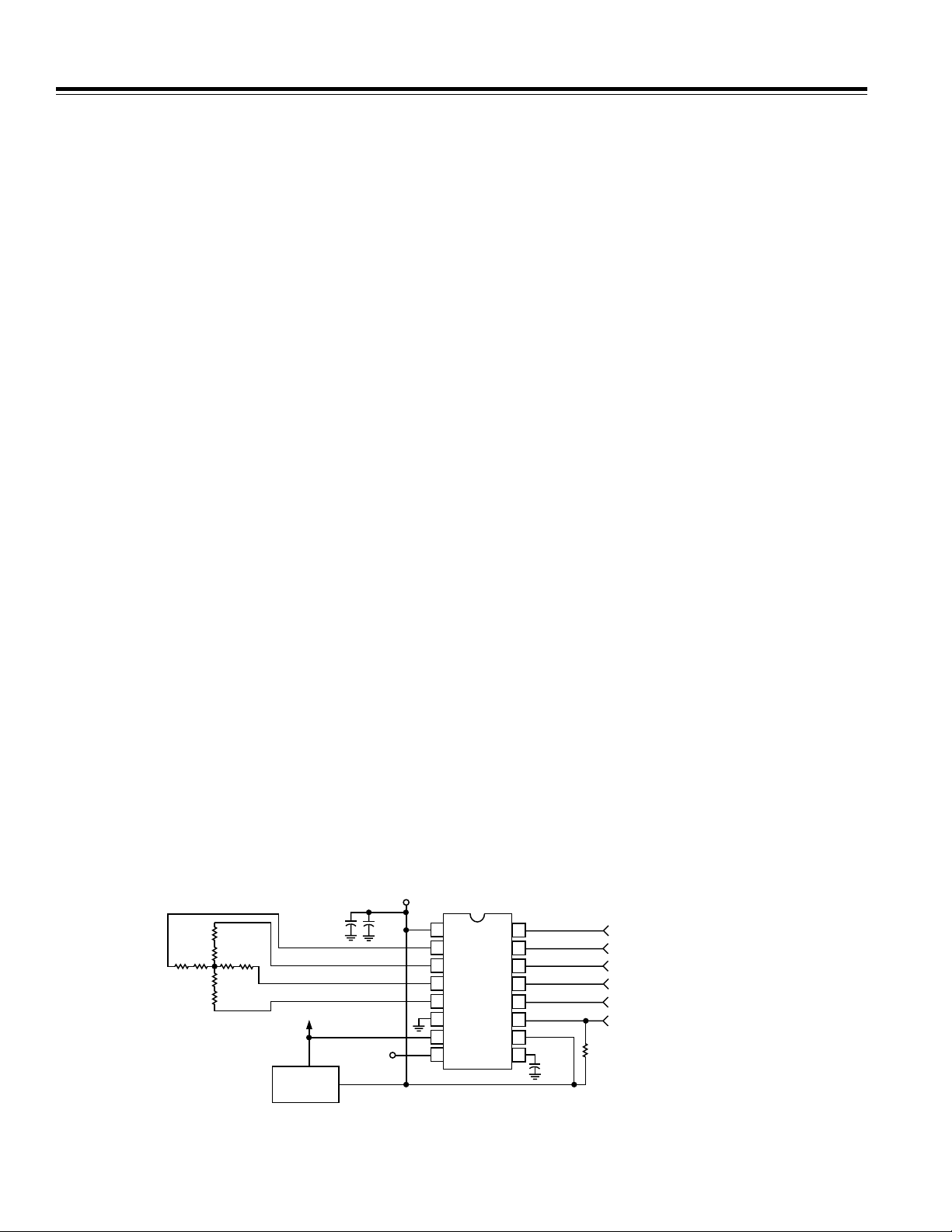
Typical Connection Diagram
Figure 1 shows a typical connection diagram for the
AD7873 in a touch screen control application. The
AD7873 features an internal reference but this can be
overdriven with an external low impedance source
between 1 V and +V
. The value of the reference volt-
CC
age will set the input range of the converter. For more
information concerning this device, refer to the AD7873
data sheet. For further evaluation information refer to
the AD7873 evaluation board and documentation.
C02485–2.5–5/01(0)
TOUCH
SCREEN
1F TO 10F
(OPTIONAL)
TO BATTERY
VOLTAGE
REGULATOR
AUXILIARY
INPUT
2.2V TO 5V
0.1F
1
2
3
4
5
6
7
8
AD7873
+V
CC
X+
Y+
X–
Y–
GND
V
BAT
AUX
DCLK
CS
DIN
BUSY
DOUT
PENIRQ
+V
V
REF
16
15
14
13
12
11
10
CC
9
Figure 1. AD7873 Typical Application Circuit
–2–
0.1F
SERIAL/CONVERSION CLOCK
CHIP SELECT
SERIAL DATA IN
CONVERTER STATUS
SERIAL DATA OUT
PEN INTERRUPT
50k⍀
PRINTED IN U.S.A.
REV. 0
 Loading...