

AN-573
a
APPLICATION NOTE
One Technology Way • P.O. Box 9106 • Norwood, MA 02062-9106 • Tel: 781/329-4700 • FAX: 781/326-8703 • www.analog.com
OP07 Is Still Evolving
by Reza Moghimi
INTRODUCTION
The OP07 has been tinkered with over the years, and versions of it are still available in plastic packages.
This application note highlights some of the major features
that the OP17x7 brings into new designs. A number of
applications using these features are presented.
SINGLE-SUPPLY OPERATION
One of the biggest problems with the part in today’s
environment is that the OP07 requires dual supplies. A
new family of amplifiers from Analog Devices addresses
this problem while still giving a close replica of the
original specifications. The OP777 single, OP727 dual,
and OP747 quad operational amplifiers allow supplies
from ±15 V down to ±1.35 V with split rails, and from
+30 V down to +2.7 V with single rail operation. The data
sheet characterizes the parts with rails of +5 V and ±15 V.
The OP7x7 family’s true single-supply capability enables
designers to operate down to the negative supply or
ground in both single- and dual-supply applications.
5V
R4
26.7k
V2
R7
100
V1
R12
1M
GAIN = 100 (V2 – V1)
R4
10.1k
U4
1/4
OP747
R14
10.1k
U3
1/4
OP747
R15
1M
AD589
R3
37.4k
D1N
V+
3
U1
2
V–
2.55M
1
1/4
OP747
R8
R2
200
RTD
100
R5
26.7k
6.19k
R9
V
OUT
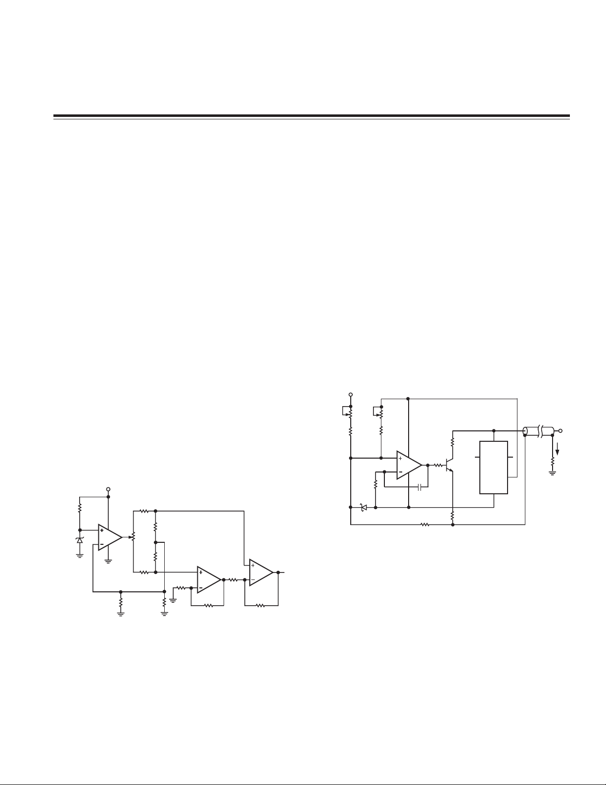
Figure 1 shows that the gain of the instrumentation amplifier (made up of U3 and U4) is set for 100. The AD589
establishes 1.235 V while the U1 amplifier servos the
bridge while maintaining the voltage across the parallel
combination of 2.55 MΩ and 6.19 kΩ to generate a 200 µA
current source. This current splits evenly and flows into
both halves of the bridge, eventually through RTD, and
establishes an output voltage based upon its value.
As shown in Figure 2, the circuit floats up from the
single-supply (12 V to 30 V) return. It consumes only
1.5 mA, leaving 2.5 mA available to the user for powering other signal conditioning circuitry.
VIN 0V TO 3V
R23
10k
R21
182k
HP5082-2800
R24
100k
R20
1.21M
V+
OP777
3
1
2
R22
1k
D2
2
1
V–
C2
220pF
R28
100k
R25
220
R26
100
Q1
2N1711
REF-02A/D
R27
10k
2
V
IN
3
TRIM
V
GND
OUT
4
5
6
T1
TWIST
PAIR
R29
100
12V TO
30V
420
mA
Figure 2. Self-Powered 4–20 mA Current Loop
Transmitter
Figure 1. Low Power Single-Supply RTD Amplifier
REV. A
AN-573
+V
S
2
V
IN
REF192
V
GND
4
OUT
+V
S
6
C7
0.1F
V+
3
1
2
1/4
R1
V–
OP747
R1(1+)
R2
R1(1+)
R1
REF192
+V
2
V
IN
GND
4
A = 300
AR1V
REF
=
V
OUT
S
R84
1M
6
V
OUT
2R2
OP747
R82
10.1k
1/4
+2.5V
R85
10k
R91
10.1k
1/4
OP747
R83
1M
V
OUT
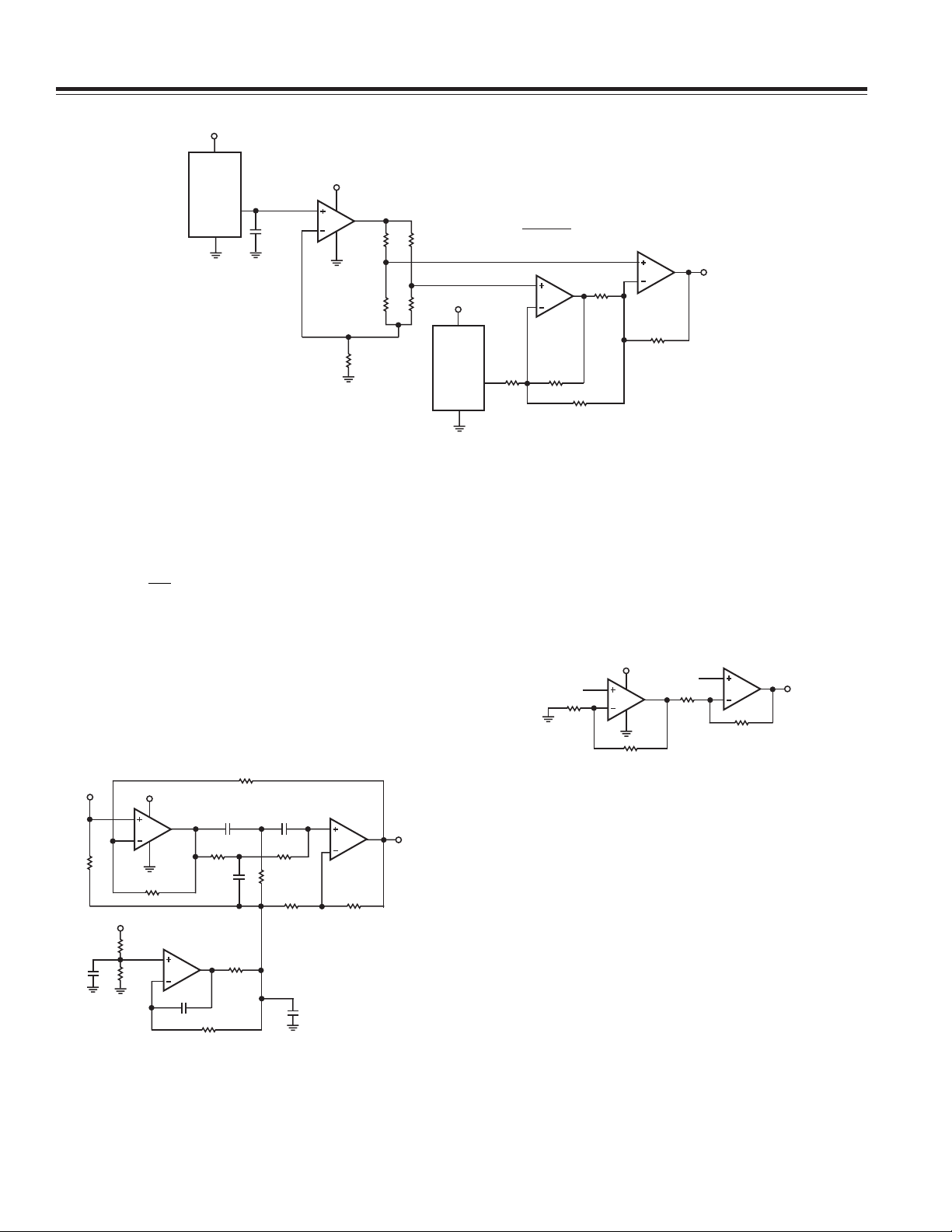
Figure 3. Single-Supply Linear Response Bridge
The OP7x7 is very useful in many bridge applications.
Figure 3 shows a single-supply bridge circuit whose output is linearly proportional to the fractional deviation ()
of the bridge.
R
Note that
=
R
To process ac signals in single-supply systems, it is
often best to use a false-ground biasing scheme. This
is shown in Figure 4, done by amplifier A3. The user
should replace the 2.67 kΩ Twin-T section with a 3.16 kΩ
resistor to reject 50 Hz. Sensitivity is due to the
relative matching of the capacitors and resistors in
the Twin-T section. Use Mylar (5%) and 1% resistors
for satisfactory results.
100k
1F
V
IN
+3V
3
2
1M
1M
+3V
V+
V–
2.67k
1
1/4
OP747
0.01F
1/4
OP747
2.67k
100k
2F
1F
499
2.67k
1F
2.67k
1.33k
1k
1F
1/4
OP747
1k
V
OUT
Figure 4. 3 V Single-Supply 50 Hz/60 Hz Active Notch
Filter with False Ground
MUCH LOWER SUPPLY CURRENTS
The OP07 has a quiescent current that is higher than
desired in today’s portable applications. The quiescent
current of the OP777 in-amplifier is less than 350 µA,
while the old OP07 required 4 mA for ±15 V operation. In
terms of power consumption, the new part wins hands
down. This allows the part to be designed into many
portable applications.
V1
R12
1M
3
2
5V
V+
U4
V–
R14
10.1k
1
1/2
OP727
V2
R13
10.1k
U3
R15
1M
1/2
OP727
V
OUT
Figure 5. Single-Supply Micropower In-Amp
OP727 can be used to build an instrumentation amplifier
(IA) with two op amps. A single-supply instrumentation
amplifier using one OP727 amplifier is shown in Figure
5. For true difference, R14/R12 = R15/R13. The formula
for the CMRR of the circuit at dc is CMRR = 20 × log (100/
(1 – (R15 × R14)/(R13 × R12)). It is common to specify the
accuracy of the resistor network in terms of resistor-toresistor percentage mismatch. The CMRR equation can
be rewritten to reflect this CMRR = 20 × log (10000/%
mismatch). The key to high CMRR is a network of resistors that is well matched from the perspective of both
resistive ratio and relative drift. It should be noted that
the absolute value of the resistors and their absolute
drift are of no consequence. Matching is the key. CMRR
is 100 dB with a 0.1% mismatched resistor network. To
maximize CMRR, one of the resistors such as R12
should be trimmed. Tighter matching of two op amps
in one package (OP727) offers a significant boost in
performance over the triple op amp configuration. For
–2–
REV. A
AN-573
this circuit, V
≤ 290 mV, 2 mV ≤ V
= 100 (V2 – V1) for 0.02 mV ≤ (V1 – V2)
O
≤ 29 V.
OUT
Due to its great dc accuracy and specification, the OP747
can be used to create a multiple output tracking voltage
reference from a single source, as shown in Figure 6.
+15V
22k
AD680AD
2
V
IN
TEMP
GND
4
IN4002
1F
+V
R48
R49
10k
6
V
OUT
3
10k
2F
C8
1F
3
2
V–
R50
10k
S
V+
OP747
1
1/4
OP747
10k
10k
1/4
10k
OP747
10k
1/4
1/4
OP747
10V
7.5V
5V
2.5V
Figure 6. Multiple Output Tracking Voltage Reference
Figure 7 shows an example of a 5 V, single-supply current
monitor that can be incorporated into the design of a
voltage regulator with foldback current limiting or a
high current power supply with crowbar protection. The
design capitalizes on the OP777’s common-mode range
that extends to ground. Current is monitored in the
power supply return where a 0.1 Ω shunt resistor, R
SENSE
creates a very small voltage drop. The voltage at the
inverting terminal becomes equal to the voltage at the
noninverting terminal through the feedback of Q1,
which is a 2N2222 or equivalent NPN transistor. This
makes the voltage drop across R1 equal to the voltage
drop across R
. Therefore, the current through Q1
SENSE
becomes directly proportional to the current through
R
, and the output voltage is given by: V
SENSE
(R2/R3) × R
with I
increasing, so V
L
× IL). The voltage drop across R2 increases
SENSE
decreases with higher supply
OUT
OUT
= 5 V –
current being sensed. For the element values shown, the
V
is 2.5 V for a return current of 1 A.
OUT
Figure 8 shows the OP777 configured as a simple
summing amplifier. The output will be the sum of V1
and V2.
+15V
3.3k
10k
V1
10k
V2
V+
3
OP777
1
V
2
V–
–15V
10k
OUT
Figure 8. Summing Amplifier
ABSENCE OF CLAMPING DIODES AT THE INPUTS
The large differential voltage capability allows for operation of the parts in both rectifier circuits and precision
comparator applications. The need for external clamping diodes (on-board in the OP07) is eliminated; such
diodes are often needed on precision op amps and are
the bane of many comparator designs.
The simple oscillator shown in Figure 9 creates a square
wave output of ±V
at 1 kHz for the values shown.
S
Other oscillation frequencies can be derived using
f = 1/(2R3 × C10 × ln ((R61 + R60)/R61).
R61
100k
+V
R60
100k
,
C10
0.01F
S
3
V+
1
V
2
OP777
V–
–V
S
R3
68k
OUT
V
= (VS) @ 1kHz
OUT
Figure 9. Free-Running Square Wave Amplifier
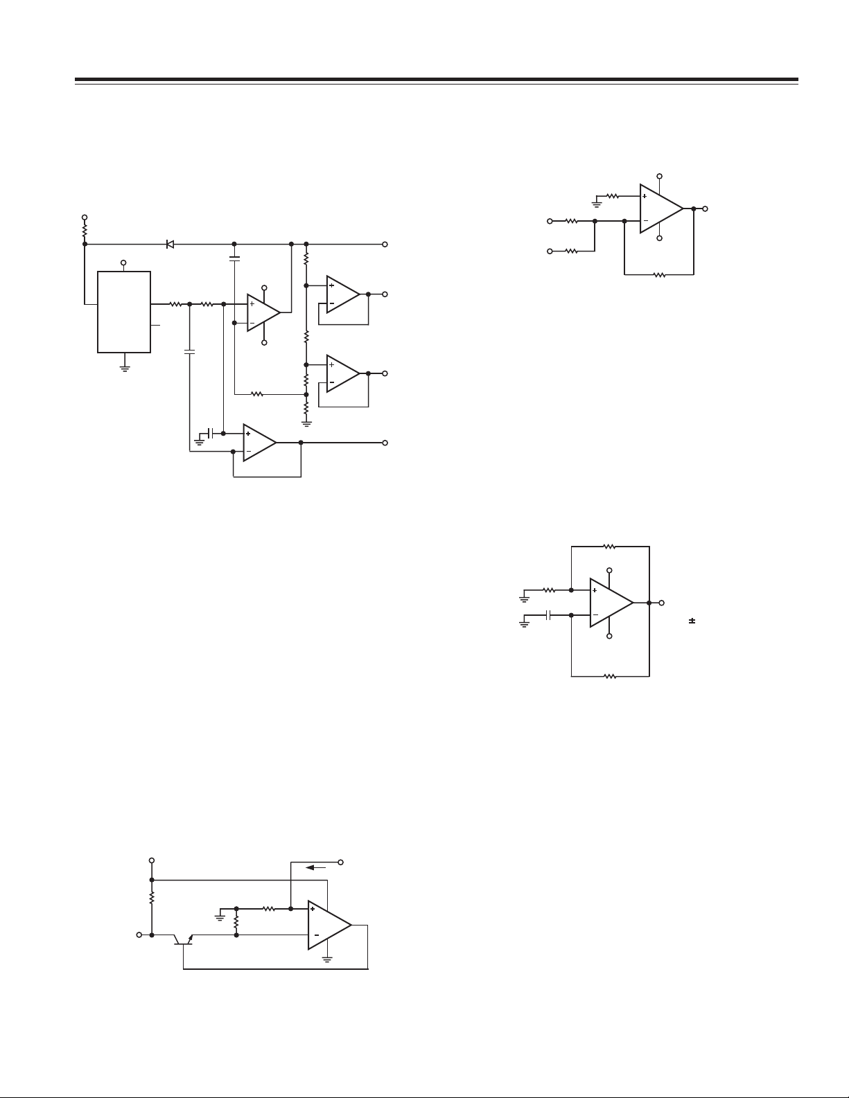
The programmable window comparator is capable of
12-bit accuracy. DAC8212 is used in the voltage for setting the upper and lower thresholds.
5V
R
R3
100
SENSE
0.1
R2
2.49k
Q1
OUT
2N2222A/ZTX
V
Figure 7. Low-Side Current Sensing Circuit
REV. A
RETURN TO
GROUND
V+
3
U1
2
V–
1
OP777
–3–
AN-573
3
2
V–
1/2
OP727
V+
1
V
IN
1/2
OP727
1k
+15V
30pF
D3
1N4148
2k
–15V
0V < V
OUT
< 10V
D3
1N4148
1k
+15V
17
GND
DB0
16
DB1
15
DB2
14
DB3
13
DB4
12
DB5
11
DB6
10
DB7
9
DB8
8
DB9
7
DB10
6
DB11
19
CS
20
WR
4
V
REF A
22
V
REF B
18
DACA
AGND
DAC8212
1
V
TEMP
I
OUTA
I
OUTB
R
FB A
R
FB B
DACB
DGND
5
OUT
REF-10/AD
2
24
3
23
3
V
IN
GND
4
V
TRIM
V
OUT
R68
10k
IN
R67
10k
5
1/2
OP727
3
V+
1
2
1N4148
1N4148
1/2
OP727
V–
–15V
10k
10k
+5V
1k
TTL OUT
2N2222A/ZTX
Figure 10. Programmable High Resolution
Window Comparator
An OP777 is used to build a precision threshold detector.
In this circuit, when V
tive, reverse biasing the diode. V
When V
(V
IN
> = VTH, the feedback occurs and V
IN
– VTH)(1 + RF/RS). C is selected to make the loop
< VTH, the amplifier swings nega-
IN
= VTH if RL = infinite.
OUT
= VTH +
OUT
respond in a smoother fashion.
+15V
2k
V
IN
V
TH
R
S
1k
V–
–15V
V+
OP777
R
100k
C
F
1N4148
V
OUT
= VTH+(V
IN – VTH
)
1+
(
R
R
F
)
S
Figure 11. Precision Threshold Detector/Amplifier
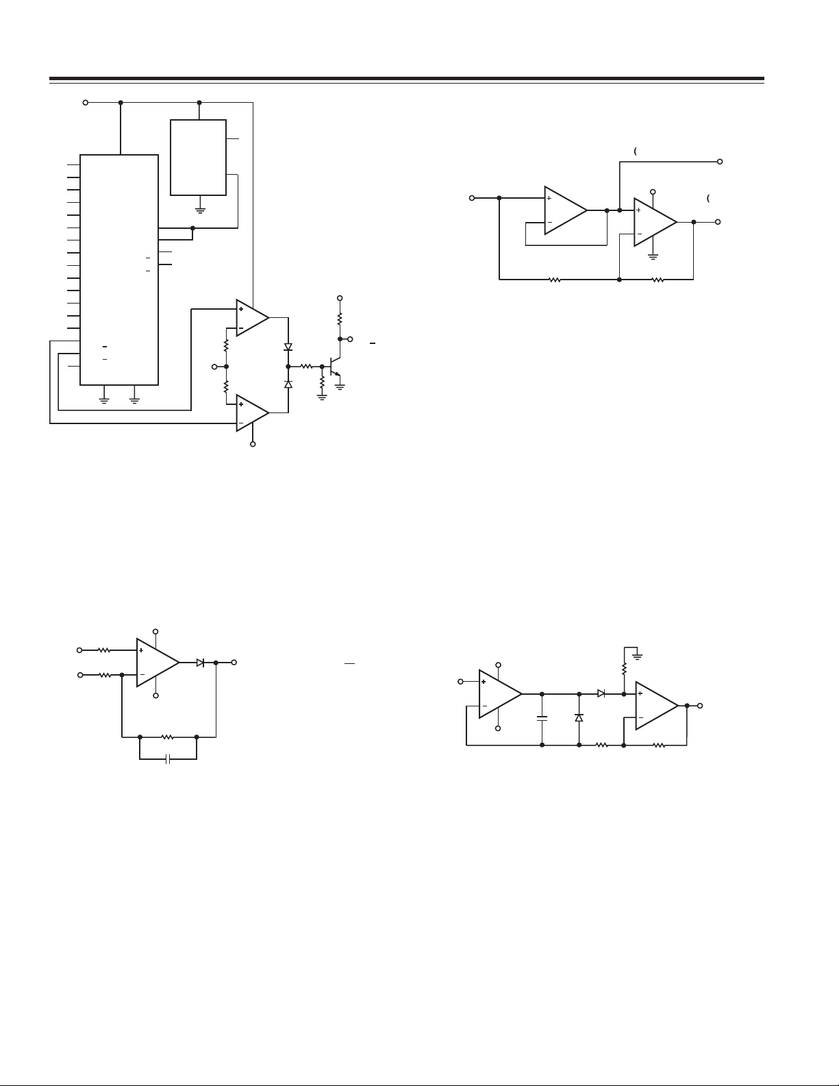
For VIN > 0 V and less than 2 kHz, there will not be any
current flow through the feedback resistors, and the output voltage tracks the input. For V
the first amplifier goes to 0 V (i.e., –V
< 0 V, the output of
IN
), which configures
S
the second amplifier in inverting follower mode. The
output is then a full-wave rectified version of the input
signal. As can be seen from the schematic, a half-wave
rectified version of the signal is also available at the output of the first amplifier.
V
HALF-WAVE RECTIFIED)
OUT
5V
FULL-WAVE
V
OUT
V+
RECTIFIED)
1/2
OP727
V–
2V p-p
3
2
100k 100k
1/2
OP727
1
Figure 12. Single-Supply Half-Wave and
Full-Wave Rectifier
RAIL-TO-RAIL OUTPUT
With light loads, the output can swing to within 1 mV of
both supply rails and the parts are stable in a voltagefollower configuration. Short-circuit protection on the
output protects the devices up to 30 mA with split ±15 V
supplies (10 mA with a single 5 V supply).
NEGATIVE RAIL INPUT
The amplifiers will respond to signals as low as 1 mV
above ground in a single-supply arrangement. The
OP7x7 family’s true single-supply capability enables
designers to operate down to the negative supply or
ground in both single- and dual-supply applications.
The high gain and low TCV
of OP727 ensures accurate
OS
operation with microvolt input signals. (See Figure 13.)
In this circuit, the input always appears as a commonmode signal to the op amps. The CMRR of the OP727
exceeds 120 dB, yielding an error of less than 2 ppm.
Figure 13. Precision Absolute Value Amplifier
A single-supply current source is shown in Figure 14.
Large resistors are used to maintain micropower operation. Output current can be adjusted by changing the
R10 resistor. Compliance voltage is
|
V
| |
V
| – |
V
|;
I
L
SAT
I
=
1 mA–11 mA; R2
OUT
S
= R2/(R8 ×
OUT
=
R10
R10
+
R7
) ×
V
;
S
–4–
REV. A

AN-573
OP777/
OP727/
OP747
V p-p = 32V
30V
2.7V TO 30V
R8
100k
C2
10pF
R9
100k
97.3k
3
2
R7
U3
V–
R6
100k
10pF
V+
OP777
C1
1
R10
2.7k
I
= 1mA–11mA
OUT
R
LOAD
Figure 14. Single-Supply Current Source
When in single-supply applications, driving motors or
actuators in two directions is often accomplished using
an H bridge (see Figure 15). This driver is capable of
driving loads from 0 V to 5 V in both directions. If this is
used to drive inductive loads, be sure to add diode
clamps to protect the bridge from inductive kickback.
5V
0V < VIN < 2.5V
1.67V
R39
5k
5V
3
V+
U3
2
1/2
OP727
V–
1
Q3
2N2222A/ZTX
V
OUT
Q4
2N2222A/ZTX
3V OVER THE INPUT
The PNP input stages are protected with 500 Ω current-
limiting resistors, allowing input voltages up to 3 V
higher than either rail without causing damage or phase
reversals. The phase reversal protection operates for
conditions where either one or both inputs are forced
beyond their input common voltage range.
INPUT
VOLTAGE (5V/DIV)
TIME (400s/DIV)
VS = 15V
A
= 1
V
OUTPUT
Figure 17. No Phase Inversion
R40
10k
R38
10k
U3
1/2
OP727
2N2907
Q5
R37
10k
2N2907
Q6
Figure 15. H Bridge
The current source shown in Figure 16 supplies both
positive and negative current into grounded load. It
should be noted that Z
R2A)/R1) – R2/R5 and that for Z
= R2B × ((R2A/R1) + 1)/((R2B +
OUT
to be infinite, there
OUT
should be (R2A + R2B)/R1 = R2/R5.
R2A
1.8k
V
R5
2k
V
IN
R1
2k
CC
7
3
V+
U1
2
V–
4
OP777
V
EE
R2
2k
6
R2B
200
R2 = R2A+R2B
I
= VIN/200
OUT
R
LOAD
Figure 18a. Unity Gain Follower
VSY = 15V
V
IN
V
OUT
VOLTAGE (5V/DIV)
TIME (400s/DIV)
Figure 18b. Input Voltage Can Exceed the Supply
Voltage without Damage
REV. A
Figure 16. Bilateral Current Source
–5–

AN-573
The dynamic performance and noise characteristics of
the devices are similar whether they are being used with
single or dual supplies. The slew rate with a 2 kΩ load is
200 mV/µs, while the gain-bandwidth product is 700 kHz.
Peak-to-peak voltage noise from 0.1 Hz to 10 Hz is 0.4 µV,
while the voltage noise density at 1 kHz is 15 nV√Hz.
The gain characteristics, of course, are rather different
at differing rails. The inputs have a maximum, single
temperature offset of 100 µV with an input offset current
of 2 nA and input bias current (I
mum. With a single 5 V rail, the common-mode rejection
ratio (CMRR) is typically 110 dB and the large signal voltage gain is typically 500 V/mV with a 10 kΩ load. With
±15 V rails, the CMRR increases, not surprisingly by
10 dB to 120 dB, and the large signal voltage gain
increases to 2500 V/mV.
For designs operating at ±15 V, the OP777 is the first
low noise precision amplifier available in the tiny
MSOP 8-lead package. The OP777 is also available in
the SOIC 8-lead surface-mount package.
This family will be extremely useful in instrumentation,
for remote sensor acquisition, and in precision filters.
The high voltage range will allow the use of the parts for
single-supply current sourcing and large range instrumentation amplifiers. Both single-supply and dual-supply
linear-response bridges can also be built. The parts are
ideal for use in low-side current monitors in power
supply control circuits since the common-mode range
extends to ground in the single-supply configuration.
DESIGN REMINDERS FOR ACHIEVING HIGH PERFORMANCE
As with any application, a good ground plane is essential
to achieve the optimum performance. This can significantly reduce the undesirable effects of ground loops
and I × R losses by providing a low impedance reference
point. Best results are obtained with a multilayer board
design with one layer assigned to the ground plane.
In order to minimize high frequency interference and
prevent low frequency ground loops, shield grounding
techniques are required when sensors are used. The
cable shielding system should include the cable end
connectors.
) of only 10 nA maxi-
B
Switching power supplies with high output noise are
normally used in many systems. This noise generally
extends over a broad band of frequencies and occurs as
both conducted and radiated noise, and unwanted electric
and magnetic fields. The voltage output noise of switching
supplies is short-duration voltage transients, or spikes
that contain frequency components easily extending to
100 MHz or more. Although specifying switching supplies in terms of rms noise is a common vendor practice,
a user should also specify the peak
of the switching spikes with the output loading of the
individual system. Capacitors, inductors, ferrite beads,
and resistors are used in filters for noise reduction. One
can also do linear post regulation and separate the
power supply circuit from sensitive analog circuits.
Analog Devices manufactures many anyCAP
linear regulators. Examples of these devices are the
ADP3300 to ADP3310 and ADP3335 to ADP3339 for supply voltages less than 12 V.
Capacitors are probably the single most important filter
component for switchers. There are generally three classes of capacitors useful in filters in the 10 kHz to 100 MHz
frequency range suitable for switchers. Capacitors are
broadly distinguished by their generic dielectric types:
electrolytic, film, and ceramic. Background and tutorial
information on capacitors can be found in the article
"Picking Capacitors"* and many vendor catalogs.
Chip capacitors should be used for supply bypassing,
with one end of the capacitor connected to the ground
plane and the other end connected within 1/8 inch of
each power pin. An additional large tantalum electrolytic capacitor (4.7 µF to 10 µF) should be connected in
parallel. This capacitor does not need to be placed as
close to the supply pins as it provides current for fast
large signal changes at the device’s output.
Use short and wide PCB tracks to decrease voltage
drops and minimize inductance. Make track widths at
least 200 mils for every inch of track length for lowest
DCR, and use 1 ounce or 2 ounce copper PCB traces to
further reduce IR drops and inductance
Be careful not to exceed the maximum junction temperature or the maximum power dissipation rating of an
amplifier. If a capacitive load is to be connected to the
output of the amplifier, be sure to include in the calculation the power dissipation caused by the rms ac
current delivered to the load.
(or p-p) amplitudes
®
low dropout
.
*Walt Jung, Dick Marsh. "Picking Capacitors," Parts 1 and 2.
(February, March 1980).
–6–
Audio
REV. A

AN-573
Use short leads or leadless components to minimize
lead inductance. This will minimize the tendency to add
excessive ESL and/or ESR. Surface-mount packages are
preferred
impedance
quency, current, and temperature variations!
Make use of vendor component models for the simulation
of prototype designs, and make sure that lab measurements correspond reasonably with
modeling is a powerful tool for predicting the performance
of analog circuits. Analog Devices provides macro models
for most of its ICs. SPICE models can be downloaded from
the ADI website (http://products.analog.com/products/
info.asp?product=OP777).
.
Use a large area ground plane for minimum
.
Know how components behave over fre-
the simulation. SPICE
Since models omit many real-life effects and no model
can simulate all of the parasitic effects of discrete
components and PCB traces, prototypes should be built
and proven before production. In order to ensure
successful prototyping, always use a ground plane for
precision or high frequency circuits. Minimize parasitic
resistance, capacitance, and inductance. If sockets are
required, use “pin sockets” (“cage jacks”). Pay equal
attention to signal routing, component placement,
grounding, and decoupling in both the prototype and
the final design. Popular prototyping techniques include
Freehand “dead-bug” using point-to-point wiring, and
Solder-Mount, milled PC board from CAD layout, multilayer boards that are double-sided with additional
point-to-point wiring.
REV. A
–7–

E02380–0–6/03(A)
© 2003 Analog Devices, Inc. All rights reserved. Trademarks and registered trademarks are the property of their respective companies.
–8–
 Loading...