

Page 1

AN-543
a
APPLICATION NOTE
One Technology Way • P.O. Box 9106 • Norwood, MA 02062-9106 • 781/329-4700 • World Wide Web Site: http://www.analog.com
High Quality, All-Digital RF Frequency Modulation Generation with the ADSP-2181
DSP and the AD9850 Direct Digital Synthesizer
by Dean R. Becker
The following describes the implementation of a high
quality all-digital FM RF generator for use with audio frequency input signals. The FM RF signal output is in the
broadcast FM band and can be monaural or stereo.
FM modulators have been with us since the time of
Major Edwin H. Armstrong (sometimes known as the
father of FM) and his classic 1936 paper on the subject.
He first put down on paper the fundamental concept of a
fixed center frequency that is varied per a constant deviation ratio that is independent of the frequency of the
modulating signal. FM became very popular because
much of the noise generated in nature exhibits AM characteristics. The signal-to-noise ratio of an FM signal will
be found to exceed that of an AM signal due to the
provement ratio
familiar with the wideband FM broadcast band and its
superior sound quality and noise immunity when compared with AM broadcast.
Analog FM modulators typically employ an oscillator
with a varactor diode in the tuned circuit. The voltage to
the varactor is varied by the modulating signal, which
changes its capacitance, therefore changing the resonant point of the oscillator’s tuned circuit, which shifts
the frequency. As noted above, constant center frequency and deviation ratio are essential to quality FM.
Much work has been done to embellish the basic oscillator circuit to provide the needed stability. Even though
complex circuitry can be added to automatically compensate for power supply and temperature variations,
these circuits still require periodic recalibration to deal
with component aging.
related to the deviation ratio. We are all
im-
Recent developments in digital signal processing (DSP)
devices have made it possible to create high quality FM
modulation using all-digital circuitry. This modulator
does not require periodic recalibration, it does not drift
with temperature or power supply variations, and it is
very easy to reproduce since there are no analog adjustments (other than the level of the input analog modulating signal). At the heart of this circuit is a Direct Digital
Synthesizer (DDS), such as the AD9850 Complete-DDS
(C-DDS) device. The AD9850 consists of a digital phase
accumulator, a phase/amplitude converter and a D/A
converter. It creates a linear ramp in the phase accumulator with a frequency that is dependent on the phase
accumulator’s input value. The ramp is mapped to a
sampled sinusoidal signal by the phase-to-amplitude
converter. The sampled digital signal is then D/A converted and filtered with a reconstruction filter to produce an analog waveform. All functions of the DDS
(except the analog reconstruction filter) are contained in
the AD9850 chip. The sampled signal is created at a
sample rate of 125 MHz, allowing high frequency RF output. Prior to the release of the AD9850, very fast, inexpensive C-DDS devices did not exist. For a more detailed
explanation of the operation and specifications of a
C-DDS device, please refer to the theory of operation in
the AD9850 data sheet.
HARDWARE IMPLEMENTATION
The implementation of the FM RF generator consists of
an Analog Devices EZ-KIT Lite 16-bit DSP development
board, some I/O decode circuitry, and an evaluation
board for the DDS—the AD9850-FSPCB as shown in
Figure 1.
AUDIO IN
L AND R
LINE IN
AD9850/FSPCB
DDS
AD9850
125MHz
XOSC
AD1847
STEREO
CODEC
EZ-KIT LITE
ADSP-2181
DSP mP
ADSP-2181
BUS
I/O DECODE
LOGIC
8-BIT
DATA
Figure 1. Block Diagram of FM RF Generator Implementation
DAC
OUT
FM RF
OUTPUT
Page 2
AN-543
AD9850-FSPCB
EVAL BOARD
MODIFIED CONNECTIONS
2
D1
3
D2
4
D3
5
D4
6
D5
7
D6
8
D7
9
D8
11
CLK
1
OE
74AC574
CONNECT DIRECTLY
TO 74AC574 PINS
2
D1
3
D2
4
D3
5
D4
6
D5
7
D6
8
D7
9
D8
11
CLK
V
CC
1
OE
74AC574
CUT OE's FROM GND
THEN TIE TO V
EZ-KIT LITE
BOARD
19
Q1
Q2
Q3
Q4
U2
Q5
Q6
Q7
Q8
D7
18
D6
17
D5
16
D4
15
D3
14
D2
13
D1
12
D0
I/O INTERFACE BOARD
19
Q1
18
Q2
17
Q3
16
Q4
U3
15
Q5
FQ
14
Q6
Q7
Q8
CLK
W
13
RESET
12
CC
UD
12
6
2
U1A
74LS10
U1B
74LS10
U2A
74LS04
1
2
13
3
4
5
1
43
U2B
74LS04
65
U2C
74LS04
D15
D14
D13
D12
D11
D10
D9
D8
IOMS
A1
WR
A0
RESET
P2-30
P2-29
P2-28
P2-27
P2-26
P2-25
P2-24
P2-23
J2-41
J2-2
J2-39
J2-1
J3-37
Figure 2. Schematic of I/O Decode Logic and Interconnections
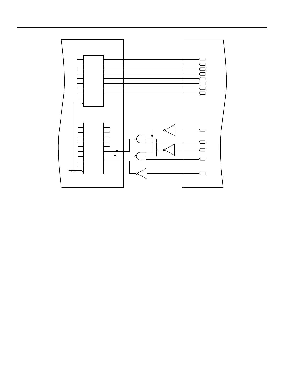
The EZ-KIT Lite contains an Analog Devices ADSP-2181
KS-133 16-bit DSP with 16K × 24 of program memory
RAM and 16K × 16 of data memory RAM.
Hardware documentation comes with the EZ-KIT Lite
development board and schematics for the AD9850
C-DDS are in the AD9850 data sheet. The I/O decode
logic and interconnections are shown in the schematic
in Figure 2.
The AD9850-FSPCB evaluation board is made to interface to the parallel port of a PC. It has a Centronics-type
connector on it and buffers to work with the parallel
port. A simple way to connect it to an external DSP is by
disabling the buffers as shown in the schematic, by disconnecting the output enables from the ground plane of
the PCB and wiring them to V
. With the buffers dis-
CC
abled, the ADSP-2181 on the EZ-KIT Lite can drive the
AD9850 data lines directly. The I/O interface in the schematic decodes I/O address 1 to create the W_CLK (write
clock) signal and I/O address 2 to create the FQ_UD (frequency update) signal. These are control signals used to
write the consecutive frequency bytes into the AD9850
and then strobe the entire 32-bit frequency word into the
operational register respectively. RESET is brought in to
initialize the AD9850. Please refer to the AD9850 data
sheet for more information on loading the C-DDS.
DSP FIRMWARE IMPLEMENTATION
Two programs are described here. The first is for a monaural FM modulator (fm_xmit.dsp) and the second is for
stereo (fmStereo.dsp). Both programs are stand-alone
single modules and can be loaded into the EZ-KIT Lite
via the serial port using the EZ-KIT Lite monitor. They
begin with codec variable initialization. The only difference here is that the codec sample rate for fm_xmit is
48 kHz while it is set to 44.1 kHz in FmStereo. (This will
be explained with the FmStereo program). This part, the
initialization code, interrupt vectors and DSP and codec
initialization, was copied from a sample program that
comes with the EZ-KIT Lite. The following partial listing
in Figure 3 describes what happens on every input
sample from the codec. First the left and right input
samples are divided by two to ensure that they do not
overflow as they are summed together. Next, a deviation value is multiplied by the previous sum and then
has a center frequency value added to the product. This
is all done in 32-bit double precision to preserve the accuracy of the C-DDS. Finally, the 32-bit frequency word
is broken into four bytes and sent to the AD9850 C-DDS.
–2–
Page 3

AN-543
.
const w_clk= 0x0001; { 9850 write clock address }
.const fq_ud= 0x0002; { 9850 frequency update address }
input_samples:
ena sec_reg; { use shadow register bank }
mr0 = dm (rx_buf + 1); { Left data in }
mr1 = dm (rx_buf + 2); { Right data in }
{ loopback inputs to outputs }
sr = ashift mr0 by -1 (hi); { scale left input by 0.5 }
af = pass sr1; { setup for add }
sr = ashift mr1 by -1 (hi); { scale right input by 0.5 }
ar = sr1 + af; { add left and right together }
dm (tx_buf + 1) = ar; { Left data out }
dm (tx_buf + 2) = ar; { Right data out }
{ same output on both channels }
mx1 = 0x004e; { MSW of peak deviation value }
mx0 = 0xa4a8; { LSW of peak deviation value }
my1 = ar; { L+R codec value (MSW only, LSW=0) }
{ 32 bit mpy with one of the LSWs=0 }
mr = mx0 * my1 (us); { codec MSW * deviation LSW }
mr0 = mr1; { shift right by 16 to align with next }
Figure 3. Partial Listing of Monaural FM Code
The signal can be received on a conventional FM radio
(mono) at 90.3 MHz. The C-DDS has an f
= 125 MHz so
S
the programmed frequency of 34.7 MHz will have its first
alias at 90.3 MHz. The first alias will be attenuated by
9.4 dB due to the sin(x)/x curve from the sampling, but
there is plenty of signal to drive an FM radio. (The alias
concept is described in Figure 5 in the AD9850 data
sheet.) Note that the C-DDS cannot have a low pass filter
with cutoff at Nyquist on its output or it will block the
first alias. A bandpass filter that passes 88 MHz to
108 MHz should be used to filter out the fundamental
and the other aliases.
The center frequency for the C-DDS for 34.7 MHz has a
32-bit value of 4710CB29H. The peak deviation of 75 kHz
is a C-DDS offset of 00275254H. The number used as the
deviation value is twice that to compensate for the fact
that the input sum was divided by two to avoid overflow. These constants are arrived at from the equation:
Value
= f /(125
MHz/2E
32) = 34.3597 ×
f(f
=125
S
MHz
The value for the transmit center frequency and deviation could be changed or stored in data memory and
could be treated as variables in the program. They could
then be changed on the fly, perhaps from I/O switches or
via the serial port as desired.
When sending I/O to the AD9850, several wait states are
used to compensate for the decode logic. At least one
cycle is needed between I/Os to the AD9850 which can
be provided by a needed instruction or a nop. The first
byte to the DDS is the phase byte and is always zero. The
frequency bytes that follow are output in order from
MSByte to LSByte.
mr1 = mr2;
mr = mr + mx1 * my1 (ss); { mpy MSWs and add previous product }
ax1 = 0x4710; { MSW of DDS center frequency }
ax0 = 0xcb29; { LSW of DDS center frequency }
ay1 = mr1; { MSW of modulated deviation }
ay0 = mr0; { LSW of modulated deviation }
ar = ax0 +ay0; { add LSWs first }
mr0 = ar, ar=ax1 + ay1 + c; { save result LSW and get sum of MSWs }
sr0 = 0; { DDS phase number = 0 }
io(w_clk) = sr0; { output first byte to DDS }
sr = lshift ar by -8 (hi); { move MSB of MSW to align with D8-D15 }
io(w_clk) = sr1; { output second byte to DDS, MSB of MSW }
nop;
io(w_clk) = ar; { output third byte to DDS, LSB of MSW }
sr = lshift mr0 by -8 (hi); { move MSB of LSW to align with D8-D15 }
io(w_clk) = sr1; { output forth byte to DDS, MSB of LSW }
nop;
io(w_clk) = mr0; { output fifth byte to DDS, LSB of LSW }
nop;
io(fq_ud) = sr0; { output latch pulse, data is irrelevant }
rti;
Stereo Implementation
The FM monaural case was actually very straightforward. Creating the signal for FM stereo is a bit more involved. First of all,
hardware
. For stereo, three signals are created and
there is no change or addition to the
summed together that then FM-modulate the DDS. The
first signal is the same as in the monaural case, the sum
of the left and right channels. The second signal is a pilot
tone at 19 kHz that has a level of 9% of the maximum
signal. The third signal is the left-minus-right channel,
double sideband suppressed, carrier modulated by a
38 kHz tone. The 38 kHz tone is generated so that it has a
rising edge at every zero crossing of the 19 kHz tone.
The multiplex of these signals has frequencies that can
extend to 53 kHz (assuming that the input signal goes up
to 15 kHz). Clearly, if we keep the 48 kHz sample rate
used in Fm_xmit, the multiplex will alias into itself. A
codec sample rate of 44.1 kHz was chosen with two in-
)
serted samples evenly spaced between. This gives a final sample rate of 132.3 kHz. The two "extra" samples
are created using the ADSP-2181 timer and some careful
coding. This sample rate provides nearly exact 16-bit
phase input values for the Numerically Controlled Oscillators (NCOs) that create the 19 kHz and 38 kHz tones.
The following assembly code shown in Figure 4 is a partial listing for the stereo FM generator. Initialization and
redundant code to the mono FM generator have been
omitted.
–3–
Page 4

AN-543
ax0 = 0;
dm(TSCALE) = ax0; { no pre-scalar }
ax0 = 251;
dm(TPERIOD) = ax0; { auto load for third interrupt }
dm(TCOUNT) = ax0;
ax0 = 0;
dm(nco_19k) = ax0; { Set accumulators. Phase of the 38 kHz NCO }
dm(nco_38k) = ax0; { must be such that the 38 kHz has a rising }
reset fl1;
{———————————————————————————————
-
- wait for interrupt and loop forever
———————————————————————————————}
main: idle; { wait for an interrupt }
call dds_out; { output previous sample to DDS }
ax0 = dm(sample_flag); { get the flag that was set during intr }
ar = tstbit 0 of ax0; { 1=codec intr, 0=timer intr }
if eq jump timer_intr; { skip the codec part if 0 }
input_samples:
{ IMPORTANT!... If you change the number of instructions up to the }
{ ena timer, you need to adjust the following TCOUNT accordingly. }
ax0 = 188; { to provide the next intr @ 44.1kHz x 3 }
dm(TCOUNT) = ax0; { this takes previous instructions and }
ena timer; { the next two intr’s are gen by timer }
ax0 = dm(rx_buf + 1); { Left data in }
dm(left) = ax0;
dm(tx_buf + 1) = ax0; { Left out loopback}
ax0 = dm(rx_buf + 2); { Right data in }
dm(right) = ax0;
dm(tx_buf + 2) = ax0; { Right out loopback}
ax0 = 3; { first of three interrupts in group }
dm(sample_number) = ax0; { initialize count }
timer_intr:
ax0 = dm(sample_number); { 2 timer interrupts after codec }
ar = ax0 - 1; { decrement count }
dm(sample_number) = ar; { save count for 3rd interrupt in group }
if ne jump ti1; { exec on second interrupt of group }
dis timer; { after third interrupt, wait for codec }
{ 19 kHz generator }
ti1: ax0 = 0x24c4; { NCO phase increment for 19 kHz }
ax0 = dm (left); { Left data in }
ay0 = dm (right); { Right data in }
ay0 = dm(nco_19k); { get 19 kHz NCO phase to update }
ar = ax0 + ay0; { add phase step for 19 kHz }
dm(nco_19k) = ar; { put accumulation back into NCO }
ax0 = ar; { prep for sine routine }
call sin; { get sine }
dm(sin_19k) = ar; { save for later }
{ 38 kHz generator }
ax0 = 0x4988; { NCO phase increment for 38 kHz }
ay0 = dm(nco_38k); { get 38 kHz NCO phase to update }
ar = ax0 + ay0; { add phase step for 38 kHz }
dm(nco_38k) = ar; { put accumulation back into NCO }
ax0 = ar; { prep for sine routine }
call sin; { get sine }
dm(sin_38k) = ar; { save for later }
{ generate the L+R and L-R signals }
ar = ax0 + ay0;
{ edge on every zero crossing transition of }
{ the 19 kHz pilot tone. }
{ putting this here gives a constant update }
{ position for the DDS with no jitter }
{ interrupt latency into account }
if av set fl1; { input overdrive indicator }
dm(LplusR) = ar;
ar = ax0 - ay0;
if av set fl1; { input overdrive indicator }
dm(LminusR) = ar; { L-R remains in ar }
{ generate the multiplex modulating signal }
mr2 = 0;
mr0 = 0;
mr1 = dm(LplusR); { baseband signal in mr }
my0 = dm(sin_38k); { 38 kHz carrier }
mr = mr + ar * my0 (ss); { DSB L-R with 38 kHz }
mx0 = dm(sin_19k); { 19 kHz carrier }
my0 = 0x0b85; { factor to get 9% of 19 kHz carrier }
mr = mr + mx0 * my0 (ss); { add in 9% of 19 khz pilot tone }
dm(dds_samp) = mr0; { save result LSW for next iteration }
dm(dds_samp+1) = mr1; { save result MSW for next iteration }
if mv set fl1; { input overdrive indicator }
jump main; { loop forever }
{——————————————————————————————————
-
- The following outputs the previously calculated sample to the DDS
- Execution time is 31+(6*W), with W=3; =49
——————————————————————————————————}
dds_out:
rts;
{ create 32 bit deviation value }
mx1 = 0x0027; { MSW of peak deviation value }
mx0 = 0x5254; { LSW of peak deviation value }
my1 = dm(dds_samp+1); { L+R, (L-R)@38K, & 19k }
my0 = dm(dds_samp); { 32 bit mpy }
mr = mx0 * my0 (uu); { mpx LSW * deviation LSW }
mr0 = mr1; { shift right by 16 to align with next }
mr1 = mr2;
mr = mr + mx1 * my0 (su);{ mpx LSW * deviation MSW }
mr = mr + mx0 * my1 (us);{ mpx MSW * deviation LSW }
mr0 = mr1; { shift right by 16 to align with next }
mr1 = mr2;
mr = mr + mx1 * my1 (ss);{ mpy MSWs and add previous product}
{ add the 32 bit center frequency }
ax1 = 0x4710; { MSW of DDS center frequency }
ax0 = 0xcb29; { LSW of DDS center frequency }
ay1 = mr1; { MSW of modulated deviation }
ay0 = mr0; { LSW of modulated deviation }
ar = ax0 +ay0; { add LSWs first }
mr0 = ar, ar=ax1 + ay1 + c; { save result LSW and get sum of MSWs }
{ output to the DDS}
sr0 = 0; { DDS phase number = 0 }
io(w_clk) = sr0; { output first byte to DDS }
sr = lshift ar by -8 (hi);{ move MSB of MSW to align with D8-D15 }
io(w_clk) = sr1; { output second byte to DDS, MSB of MSW }
nop;
io(w_clk) = ar; { output third byte to DDS, LSB of MSW }
sr = lshift mr0 by -8 (hi); { move MSB of LSW to align with D8-D15 }
io(w_clk) = sr1; { output forth byte to DDS, MSB of LSW }
nop;
io(w_clk) = mr0; { output fifth byte to DDS, LSB of LSW }
nop;
io(fq_ud) = sr0; { output latch pulse, data is irrelevant }
{ reset by pressing interrupt (IRQE) }
Figure 4. Partial Listing of Assembly Code for Stereo FM Generator
–4–
Page 5
AN-543
MHz
20
–60
dBc
90.3
10
–20
–30
–40
–50
0
–10
34.7
0 20 40 60 80 100 120 140 160
At the beginning of the code, the ADSP-2181 internal
timer is set to have no prescaler and to interrupt 251
clock cycles after the last timer interrupt. This places two
timer interrupts between each codec interrupt. More on
this later. The firmware NCOs for the internally generated 19 and 38 kHz carriers are also initialized so t they
have the proper phasing as previously explained. The
routine then enters the main loop, which executes once
per interrupt. First in the loop is a call to the DDS output
routine. By calling the DDS output routine at the same
point after the interrupt, no jitter is created on the output
signal. This subroutine is similar to the one in fm_xmit,
but operates on a full 32-bit sample from the multiplex
generator. In the fm_xmit routine the input samples
were only 16 bits. The deviation value 0x00275254 is
equivalent to 75 kHz. The rest of the DDS output routine
operates as in fm_xmit.
The routine then determines if the interrupt was caused
by the codec or the timer by the use of a flag
(sample_flag) set in the interrupt routine. If the interrupt
was from the codec, the timer is initialized and starts to
create the next interrupt. This is done with a count of
188, which compensates for the instructions already executed since the interrupt. This gives the effect of 251
cycles between interrupts. Note that the selection of this
timer value is very critical to create evenly spaced interleaved interrupts. At this point left and right input signals are retrieved from their DM locations (and output
back out of the codec for a sanity check) and the sample
number is set to three to start the interrupt interleave
process.
Next the multiplex is generated. First the left-plus-right
signal is recalled and added to the product of the leftminus-right times the 38 kHz carrier. This product created the DSB modulation about 38 kHz for the difference
signal. The sum is then added to the product of the
19 kHz signal times the constant 0x0b85, which yields
the 9% 19 kHz reference carrier. The multiplex sample is
then stored for output after the next interrupt, and the
loop returns to idle to wait for the next interrupt.
This routine is an example of multirate processing. It
demonstrates the capability of the ADSP-2181 and the
flexibility of the AD9850. Even with the additional code
required for the FM stereo multiplex, there is still room
for more. One other possibility is the addition of an SCA
multiplex added into the stereo multiplex as is done in
many FM broadcasts. For this the sample rate must be
further increased and the carrier for the SCA created in a
similar fashion to the 19 kHz and 38 kHz carriers.
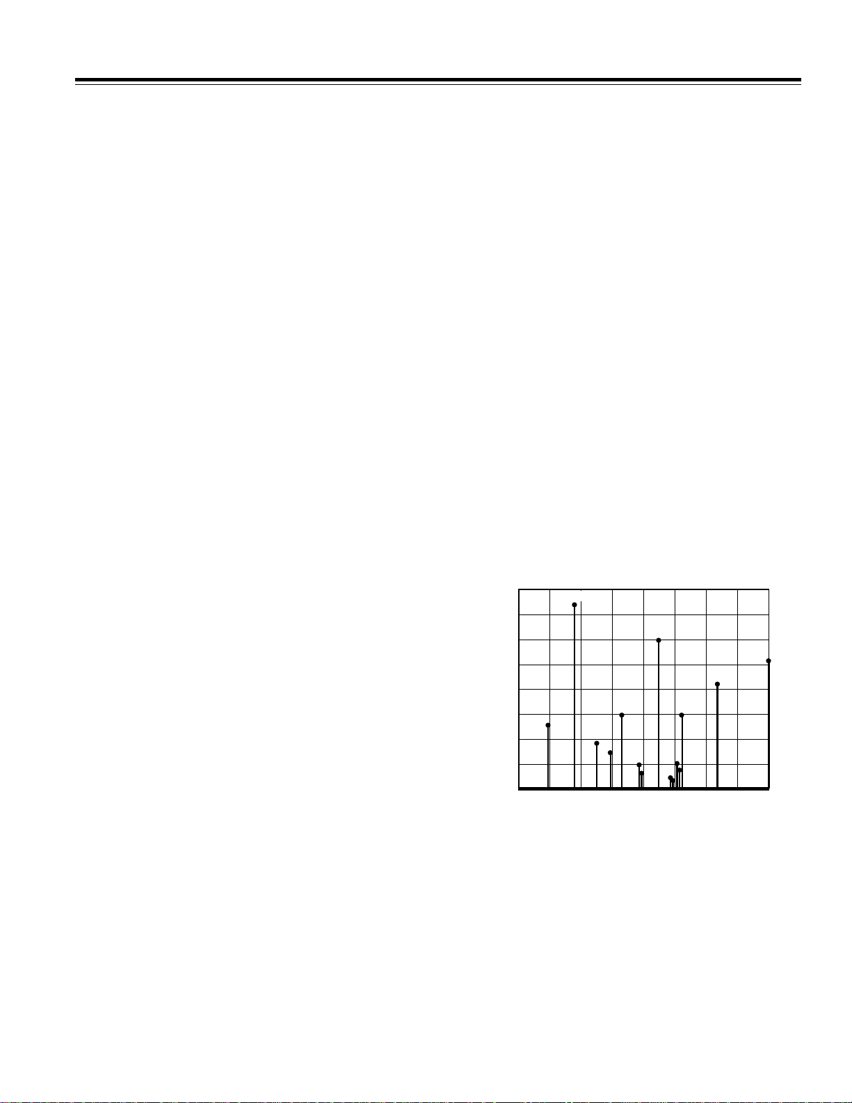
Dynamic Performance
A graph of the spurious performance of the direct DAC
output of the AD9850 is shown in Figure 5. First, there
was no shielding on the breadboard prototype so some
pickup was likely. The first point is that there appears to
be clock feed through at 125 MHz and possibly at half of
that frequency. When operating at a frequency near
40 MHz, the AD9850 is anticipated to have spurs that are
–45 dBc. Figure 5 shows that this is in fact the case.
The routine then falls into the housekeeping function for
timer interrupts. Sample_number is decremented to
two. On the next pass through this routine (caused by
the first timer interrupt) the sample_number will be decremented to one and the timer will autoload. On the
third pass, the sample_number will be decremented to
zero and this will cause the timer to be shut off. The
cycle then repeats with the next interrupt coming from
the codec.
The code that follows this is executed by all interrupts. It
first creates the 19 kHz carrier by incrementing the
19 kHz NCO, and then creates the sine carrier by using
the sin routine copied from the Analog Devices Applications Handbook, Volume 1. This routine uses a power
series to approximate the sine of the NCO phase angle.
The 38 kHz carrier is then generated in the same fashion
but with a NCO phase increment twice that of the 19 kHz
generator. The sum and difference of the left and right
signals is then created and checked for overflow. Overflow will light the red LED on the EZ-KIT Lite board to
indicate the condition. The light must be manually extinguished by pressing the interrupt button.
Figure 5. Typical DDS Output Spurious Performance
Notice that the first alias at 90.3 MHz is about 12 dB
down from the fundamental at 30.4 MHz. This is close to
what was calculated from the (sin x)/x curve mentioned
earlier. There are spurs only 30 dB down with respect to
the signal at 90.3 MHz, but they are at least 15 MHz away
and could be conventionally filtered. It was also found
(not on the graph) that there were numerous spurs in
48 kHz increments from 90.3 MHz that went out to
±300 kHz of it. These were –55 dB with respect to the
90.3 MHz signal. Outside of this range to the first spur
–5–
Page 6

AN-543
from 90.3 MHz (which is 7 MHz away) all energy was
found to be 60 dB down with respect to the 90.3 MHz
signal.
As a point of reference, the 1982 Reference Data For Radio Engineers states on page 30-6 that acceptable performance for an FM broadcast station with respect to
out-of-band radiation is that between 120 kHz and 240 kHz
from carrier, emissions should be –25 dBc. From 240 kHz
and 600 kHz it should be –35 dBc and beyond 600 kHz,
–80 dBc or 43 + 10 log P, where P is the transmitter
power in watts. Considering the measurements above,
it seems that conventional lumped-element filtering
would clean up the AD9850’s output signal to broadcastquality limits. Another possibility would be to use SAW
filters; in view of the high level of output available from
the AD9850, losses in the SAW could be compensated
for without degrading SNR.
E3362–5–9/98
–6–
PRINTED IN U.S.A.
 Loading...