

Page 1
AN-539
a
APPLICATION NOTE
One Technology Way • P.O. Box 9106 • Norwood, MA 02062-9106 • 781/329-4700 • World Wide Web Site: http://www.analog.com
Errors and Error Budget Analysis in Instrumentation Amplifier Applications
by Eamon Nash
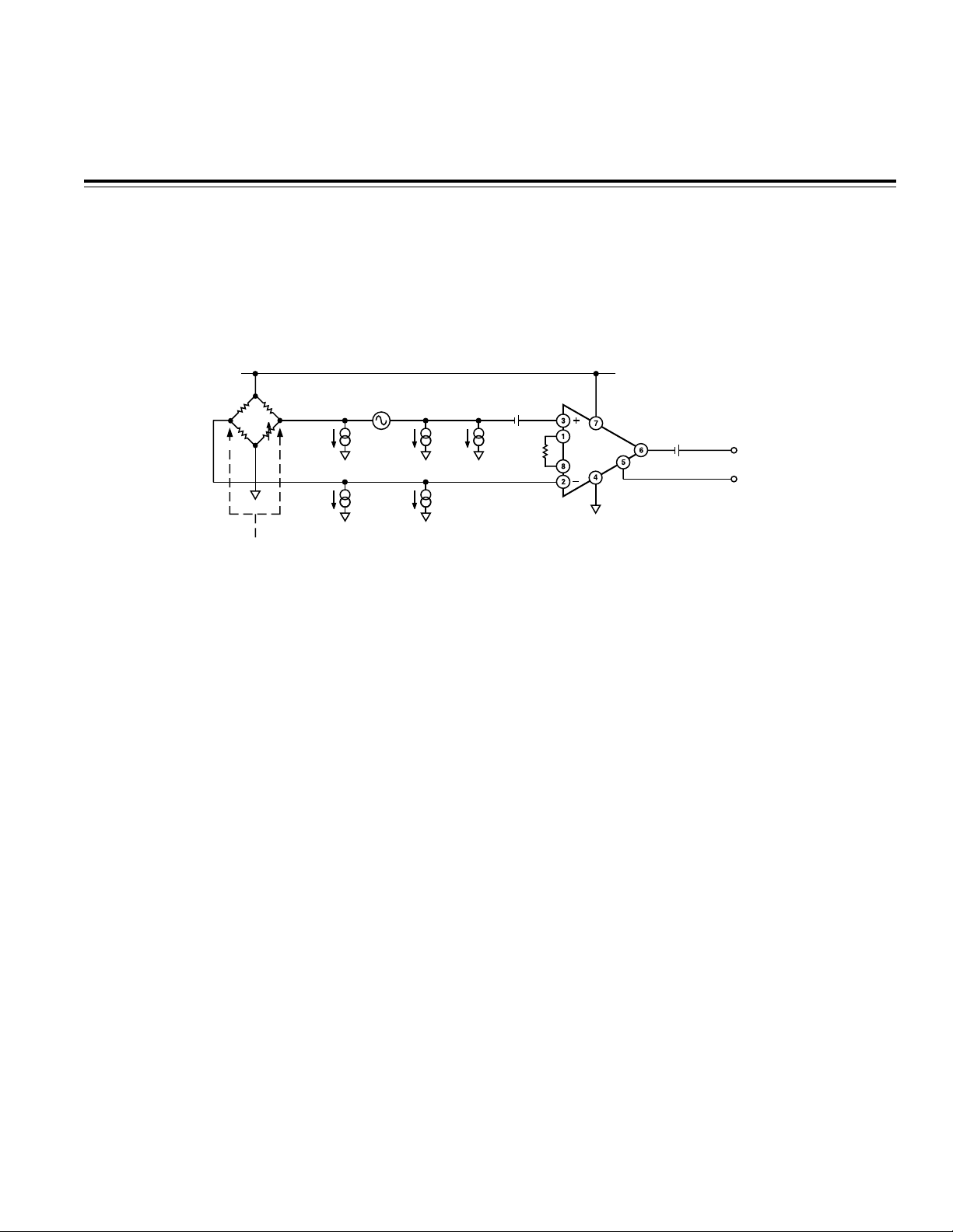
+V
S
V
NOISE
+
–
I
BIAS
I
BIAS
I
OFS
VOSIN
R
GAIN
AD623
VOSOUT
V
OUT
REFERENCE
350V
V
CM
350V350V
I
NOISE
I
NOISE
= +VS/2
Figure 1. Error Sources in a Typical Instrumentation Amplifier
INTRODUCTION
This application note describes a systematic approach
to calculating the overall error in an instrumentation
amplifier (in amp) application. We will begin by describing the primary sources of error (e.g., offset voltage,
CMRR, etc.) in an in amp. Then, using data sheet specifications and practical examples, we will compare the
accuracy of various in amp solutions (e.g., discrete vs.
integrated, three op amp integrated vs. two op amp
integrated).
Because instrumentation amplifiers are most often used
in low speed precision applications, we generally focus
on dc errors such as offset voltage, bias current and low
frequency noise (primarily at harmonics of the line frequency of either 50 Hz or 60 Hz). We must also estimate
the errors that will result from sizable changes in temperature due the rugged and noisy environment in
which many in amps find themselves.
It is also important to remember that the effect of particular error sources will vary from application to application. In thermocouple applications, for example, the
source impedance of the sensor is very low (typically
not greater than a few ohms even when there is a long
cable between sensor and amplifier). As a result, errors
due to bias current and noise current can be neglected
when compared to input offset voltage errors.
RTO and RTI
Before we consider individual error sources, understanding of what we mean by RTO and RTI is important.
In any device that can operate with a gain greater than
unity (e.g., any op amp or in amp), the absolute size of
an error will be greater at the output than at the input.
For example, the noise at the output will be the gain
times the specified input noise. We must, therefore,
specify whether an error is referred to the input (RTI) or
referred to the output (RTO). For example, if we wanted
to refer output offset voltage to the input, we would simply divide the error by the gain, i.e.,
Output Offset Error (RTI) = VOSOUT/Gain
Referring all errors to the input, as is common practice,
allows easy comparison between error sizes and the size
of the input signal.
Parts per Million—PPM
Parts per million or ppm is a popular way of specifying
errors that are quite small. PPM is dimensionless so we
must make the error relative to something. In these
examples, it is appropriate to compare to the full-scale
input signal. For example, the input offset voltage,
expressed in ppm, is given by the equation:
Input Offset Error (ppm) = (VOS/V
IN FULL SCALE
) ×
10
6
Page 2

AN-539
V
Gain V
CMRR
20
OUT
CM
–1
=
×
log
Error Sources in Discrete and Integrated Instrumentation
Amplifiers
Figure 1 shows the most common and prevalent error
sources in discrete and integrated in amps. These error
sources are detailed individually below
.
Offset Voltage
Offset voltage results from a mismatch between transistor V
s in an amplifier’s input stage. This voltage can be
BE
modeled as a small dc voltage in series with the input
signal, as shown in Figure 1. Like the input signal, it will
be amplified by the gain of the in amp. In the case of in
amps with more than one stage (e.g., the classic three
op amp in amp) the input transistors of the output stage
will also contribute an offset component. However, as
long as the output stage has gain of unity, as is generally
the practice, the in amp’s programmed gain will have no
effect on the absolute size of the output offset error.
However, for error computation, this error is usually
referred back to the input so that its effect can be compared to the size of the input signal. This yields the
equation:
Total Offset Error (RTI) = V
OS_IN
+ V
OS_OUT
/Gain
From this equation, it is clear that the effect of output
offset voltage will decrease as the in amp’s programmed gain increases.
current times the source impedance. Because either of
the bias currents can be the greater, the offset current
can be of either polarity.
Common-Mode Rejection
An ideal in amp will amplify the differential voltage between its inverting and noninverting inputs regardless
of any dc offsets appearing on both inputs. So any dc
offset appearing on both inputs (+V
/2 in Figure 1) will
S
be rejected by the in amp. This dc or common-mode
component is present in many applications. Indeed,
removing this common-mode component is often the
primary function of an instrumentation amplifier in an
application.
In practice, not all of the input common-mode signal
will be rejected and some will appear at the output.
Common-mode rejection ratio is a measure of how well
the instrumentation amplifier rejects common-mode
signals. It is defined by the formula:
CMRR (dB) 20
=×
log
Gain V
V
×
OUT
CM
We can rewrite this equation to allow calculation of
the output voltage that results from a particular input
common-mode voltage.
Offset and Bias Currents
Bias currents flow into or out of the in amp’s inputs.
These are usually the base currents of npn or pnp transistors. These small currents will therefore have a defined polarity for a particular type of in amp.
Bias currents generate error voltages when they flow
through source impedances. The bias current times the
source impedance generates a small dc voltage which
appears in series with the input offset voltage. However
if both inputs of the in amp are looking at the same
source impedance, equal bias currents will generate a
small common-mode input voltage (typically in the µV
range) that will be well suppressed by any device which
has reasonable common-mode rejection. If the source
impedances of the in amp’s inverting and noninverting inputs are not equal, the resulting error will be
greater by the bias current times the difference in the
impedances.
AC and DC Common-Mode Rejection
Poor common-mode rejection at dc will result in a dc offset at the output. While this can be calibrated away (just
like offset voltage), poor common-mode rejection of ac
signals is much more troublesome. If, for example, the
input circuit picks up 50 Hz or 60 Hz interference from
the mains, an ac voltage will result at the output. Its
presence will reduce resolution. Filtering is a solution
only in very slow applications where the maximum frequency is much less than 50 Hz/60 Hz.
Table I shows the output voltages of two in amps, the
AD623 and the INA126, that result when a 60 Hz
common-mode voltage of 100 mV amplitude is picked
up by the input.
We must also consider the offset current, which is the
difference between the two bias currents. This difference will generate an offset type error equal to the offset
Table I. Effect of CMRR on Output Voltage of AD623 and INA126 for a 60 Hz, 100 mV Amplitude Common-Mode Input
Gain VIN (cm) CMRR–INA126 CMRR–AD623 V
–INA126 V
OUT
10 100 mV @ 60 Hz 83 dB 100 dB 70.7 µV 10 µV
100 100 mV @ 60 Hz 83 dB 110 dB 707 µV 31.6 µV
1000 100 mV @ 60 Hz 83 dB 110 dB 7.07 mV 316 µV
–2–
–AD623
OUT
Page 3

AN-539
Noise
While offset voltages and bias currents ultimately lead
to offset errors at the output, noise sources will degrade
the resolution of a circuit. There are two noise sources in
most amplifiers, voltage noise and current noise. As is
the case with offset voltage and bias current, the degree
to which these sources affect the resolution varies with
the application.
1000
100
VOLTAGE NOISE – nV/ Hz
10
11k10
GAIN = 1
GAIN = 10
100
FREQUENCY – Hz
Figure 2. Voltage Noise Spectral Density of a Typical In
Amp
The voltage noise spectral density of a typical in amp
is shown in Figure 2 (a plot of current noise spectral density would have a similar characteristic). While the
response is flat at higher frequencies (above about
100 Hz, the so-called 1/f frequency), the noise spectral
density increases as the frequency approaches dc. To
calculate the resulting RTI rms noise, the noise spectral
density is multiplied by the square root of the bandwidth
of interest. The bandwidth may be the bandwidth of the
in amp at that particular gain or it may be something
less. For example, if the output signal from the in amp is
low pass filtered, the corner frequency of the filter will
define the bandwidth of interest. Note that if the output
of the instrumentation amplifier is being digitized in an
analog-to-digital converter (ADC), any post filtering
should also be factored into calculating the bandwidth
of interest.
In high frequency applications, low frequency noise
generally can be neglected. So the RTI rms noise would
simply be the product of the “flat” noise spectral density
and the square root of the bandwidth. Note that the calculated rms noise must be converted to peak-to-peak by
multiplying the rms value by 6.6
1
. For low frequency applications, data sheets usually specify peak-to-peak
noise in the 0.1 Hz to 10 Hz frequency band. If high
frequency noise is filtered at some point in the system, it
can be neglected so that only the 0.1 Hz to 10 Hz noise is
counted.
Because voltage and current noise are uncorrelated (i.e.,
are random and bear no relationship to one another),
the overall error due to noise should not be simply the
sum of all noise errors. It is more accurate to do a rootsum-square calculation of the total noise error.
Total noise
=
Voltage Noise
2
+
R
SOURCE
×
Current Noise
2
Linearity
This error will generally be specified in ppm (for a particular input span) in the data sheets of integrated instrumentation amplifiers. In the case of discrete in
amps, built from op amps, the nonlinearity is more difficult to calculate. Op amp data sheets generally do not
specify linearity. Furthermore, even if the linearity of
one op amp is known, it is necessary to estimate how
the two or three op amps will interact to give an overall
linearity specification. In many cases, the only option is
to measure the linearity of the circuit by doing a
dc sweep. The linearity in ppm will be given by the
expression.
Nonlinearity (ppm) = (Maximum deviation of output
voltage from ideal/gain/full-scale input
) × 10
6
Gain Error
The gain error of an integrated instrumentation amplifier will have two components, internal gain error and
error due to the tolerance of the external gain setting
resistor. While a precision external gain resistor will prevent the overall gain from degrading, there is little point
in wasting cost on an external resistor which is much
more accurate than the in amp’s accuracy. It is also generally difficult to achieve exactly the desired gain (e.g.,
10 or 100) when using standard resistor sizes.
It should be noted however that the choice of gain resistor can help to reduce the overall gain drift of the circuit.
As an example, let’s consider the AD623. Its gain is
given by the equation:
Gain
= 1 + (100
kΩ/RG)
The 100 kΩ value in this equation stems from two internal 50 kΩ resistors. These resistors have a temperature
coefficient of –50 ppm/°C. By choosing an external gain
resistor, which also has a negative temperature coefficient, the gain drift can be reduced.
Error Budget Analysis of Two Integrated In Amps: AD623
vs. INA126
Figure 3 shows the popular resistive bridge application.
The bridge consists of four variable resistors. The bridge
is excited by a single +5 V supply. Any change in the
resistance of the variable resistors will generate a differ-
ential voltage (±20 mV full scale) which appears across
the input of the in amp. The common-mode voltage of
the differential signal is +2.5 V. This follows from the
+5 V excitation voltage.
–3–
Page 4

AN-539
The gain of the in amp has been set so that the output
signal swing is close to its maximum level but is still not
clipping. Care should be taken not to saturate any of the
internal nodes of the in amp. This is a function of the
differential input voltage, the programmed gain and the
common-mode level
2
.
Table II shows the error budget calculations using the
integrated in amps AD623 and INA126. All errors are referred to the input (i.e., are compared to the full-scale
input voltage of 20 mV) and are then converted to parts
per million (ppm) by multiplying the fractional error by
6
1 × 10
to ppm by multiplying by 1 × 10
. Alternatively, percentage errors are converted
4
. Conversion between
fractional, percentage and ppm is shown in Table III.
350V
+5V
350V350V
350V
620 mV
RG 1.13kV
0.1% TOL
+10ppm/8C
AD623B GAIN = 89.5 (1+100kV/R
+5V
AD623B
REFERENCE
V
OUT
+2.5V
G
+5V
RG 953V
0.1% TOL
+10ppm/8C
)
INA125P GAIN = 89 (5+80kV/R
INA126P
REFERENCE
V
+2.5V
)
G
OUT
Figure 3. Amplifying the Differential Voltage from a Resistive Bridge Transducer
Table II. Error Budget Analysis: AD623 vs. INA126
AD623B INA126P Total Error Total Error
Error Source Circuit Calculation Error Calculation AD623 (ppm) INA126 (ppm)
ABSOLUTE ACCURACY at T
= +25°C
A
Input Offset Voltage, mV 100 µV/20 mV 250 µV/20 mV 5,000 12,500
Output Offset Voltage, mV 500 µV/89.5/20 mV Not Applicable 279 Not Applicable
Input Offset Current, nA 2 nA × 350 Ω/20 mV 2 nA × 350 Ω/20 mV 35 35
CMR, dB 105 dBv5.6 ppm × 83 dBv71 ppm ×
2.5 V/20 mV 2.5 V/20 mV 700 8875
Gain 0.35% + 0.1% 0.5% + 0.1% 4500 6000
Total Absolute Error 10514 27410
DRIFT TO +85°C
Gain Drift, ppm/°C (50 + 10) ppm/°C × 60°C (100 + 10) ppm/°C × 60°C 3600 6600
Input Offset Voltage, mV/°C1 µV/°C × 60°C/20 mV 3 µV/°C × 60°C/20 mV 3000 9000
Input Offset Current, pA/°C 5 pA/°C × 350 Ω × 10 pA/°C × 350 Ω ×
60°C/20 mV 60°C/20 mV 5.25 10.5
Output Offset Voltage Drift, mV/°C 10 µV/°C × 60°C/
89.5/20 mV Not Applicable 335 Not Applicable
Total Drift Error 6940 15610
RESOLUTION
Gain Nonlinearity, ppm of Full Scale 50 ppm 20 ppm 50 20
Typ 0.1 Hz–10 Hz Voltage Noise, mV p-p 1.5 µV p-p/20 mV 0.7 µV p-p/20 mV 75 35
Total Resolution Error 125 55
Grand Total Error 17579 43075
Table III. Conversion Between ppm, Fractional Error and
Percentage Error
% Error Fractional Error ppm Error
10 0.1 100000
1 0.01 10000
0.1 0.001 1000
0.01 0.0001 100
0.001 0.00001 10
0.0001 0.000001 1
Table II shows that the predominant error source is
static errors (e.g., offset voltage, etc.). In many applications where some form of calibration is available, these
errors can be removed. With the addition of some kind
of ambient temperature measurement, this calibration
can be extended to compensate for drift of static errors.
It is more difficult to compensate for errors in resolution
caused by the nonlinearity and noise of the in amp. Note
that errors due to current noise have been neglected.
–4–
Page 5

AN-539
These errors are quite small and become insignificant
when they are quadratically summed with the voltage
noise.
Additional resolution errors that occur due to external
interference cannot be characterized here. Significant in
this area is the degradation in resolution that will be
caused by common-mode pickup on the differential inputs of 50 Hz or 60 Hz interference (from lights or any
equipment running on the mains). This will result in the
50 Hz/60 Hz hum being visible on the in amp’s output.
Obviously, high common-mode rejection, not just at dc
but also over frequency, will help to minimize this interference. The common-mode rejection over frequency of
the AD623 is shown in Figure 4. This shows for example,
that the CMRR at 1 kHz, for a gain of 10, is still over
80 dB, more than sufficient for most applications.
120
110
100
90
80
70
CMR – dB
60
50
40
30
1 100k10
100 1k 10k
FREQUENCY – Hz
31000
3100
310
31
Figure 4. AD623 CMR vs. Frequency, +5 V Single
Supply, V
= 2.5 V, Gain = 1, 10, 100, 1000
REF
Make vs. Buy: A Typical Application Error Budget
The example in Figure 5 serves as a good comparison
between the errors associated with an integrated and
a discrete in amp implementation. Again, we have a
±20 mV signal we want to amplify. Using a dual op amp
and a precision resistor network, a two op amp in amp
can be implemented.
The errors associated with each implementation are detailed in Table IV and show the integrated in amp to be
more precise, both at ambient and over temperature. It
should be noted that the discrete implementation is
quite a bit more expensive (by about 100% in this example). This is primarily due to the cost of the low drift
precision resistor network.
Note, the input offset current of the discrete in amp
implementation is the maximum difference in the bias
currents of the two op amps, not the offset currents of
the individual op amps. Also, while the values of the
resistor network are chosen so that the inverting and
noninverting inputs of each op amp see the same
impedance (about 350 Ω), the offset current of each
op amp will add an additional error that must be
characterized.
350V
+5V
350V350V
350V
620mV
+5V
RG 1.13kV
0.1% TOL
+10ppm/8C
AD623A GAIN = 89.5 (1+100kV/R
AD623A
Figure 5. Make vs. Buy
V
OUT
+2.5V
G
–5–
+5V
V
OUT
1/2
OP296g
)
+2.5V
*0.1% RESISTOR MATCH, 50ppm/8C TRACKING
350V* 350V* 31.5kV*31.5kV*
“HOMEBREW” IN AMP, G = 90
1/2
OP296g
Page 6

AN-539
Table IV. Make vs. Buy Error Budget
“Homebrew” Total Error Total Error
Error Source AD623A Circuit Calculation Circuit Calculation AD623–ppm Homebrew–ppm
ABSOLUTE ACCURACY at T
Total RTI Offset Voltage, mV (200 µV+[1000 µV/89.5])/20 mV (300 µV × 2)/20 mV 10,559 30,000
Input Offset Current, nA 2 nA × 350 Ω/20 mV 100 nA × 350 Ω/20 mV* 35 1750
Internal Offset Current
(Homebrew Only) Not Applicable 16 nA × 350 Ω/20 mV* 280
CMR, dB 105 dBv5.6 ppm × 2.5 V/20 mV (0.1% Match × 2.5 V)/
Gain 0.35% + 0.1% 0.1% Match 4500 1000
DRIFT TO +85°C
Gain Drift, ppm/°C (50 + 10) ppm/°C × 60°C 50 ppm/°C × 60°C 3600 3000
Total RTI Offset Voltage, mV/°C (2 µV/°C+[10 µV/°C/89.5])
Input Offset Current, pA/°C 5 pA/°C × 350 Ω × 60°C/20 mV Not Applicable* 5.25
Internal Offset Current
(Homebrew Only) Not Applicable (120 pA/°C × 350 Ω × 2)
RESOLUTION
Gain Nonlinearity, ppm of Full Scale 50 ppm 20 ppm 50 20
Typ 0.1 Hz–10 Hz Voltage Noise,
mV p-p 1.5 µV p-p/20 mV (0.8 µV p-p × √2)/20 mV 75 56.57
*Error over temperature. bias current of OP296 is only specified as a maximum value over temperature (i.e., no value specified at + 25°C).
= +25°C
A
90/20 mV 700 1388
Total Absolute Error 15794 34418
× 60°C/20 mV (7 µV/°C × 60°C)/20 mV 6335 21,000
× 60°C/20 mV 252
Total Drift Error 9940 24252
Total Resolution Error 125 77
Grand Total Error 25859 58747
E3316a–0–8/99
REFERENCES
1.
Analog-Digital Conversion Handbook,
Third Edition, pp 550–553, by the Engineering Staff of Analog Devices, Inc., edited
by Daniel H. Sheingold, Prentice Hall, Englewood Cliffs, NJ 07632.
2. AD623 Single Supply, Rail-to-Rail, Low Cost Instrumentation Amplifier, data sheet, p 15.
PRINTED IN U.S.A.
–6–
 Loading...