Page 1

AN-536
a
APPLICATION NOTE
One Technology Way • P.O. Box 9106 • Norwood, MA 02062-9106 • 781/329-4700 • World Wide Web Site: http://www.analog.com
Dimensional Gaging Measurements with Model 3B17
Linear Variable Displacement Transducers (LVDTs) are
common in gaging systems. Two LVDTs can be used to
measure the thickness or taper of an object. For a thickness measurement, the LVDTs are placed on either side
of the object to be measured. The LVDTs are positioned
such that there is a known maximum distance between
them in the fully retracted position. When the object to
be measured is placed between the two LVDTs, the displacement of both LVDTs are added together and then
the computer or control system will subtract this total
from the known distance between the LVDTs. Taper or
slope measurements are done by positioning the two
LVDTs at the same level at a known distance apart. If the
object to be measured is on the same level as the LVDTs,
both LVDTs would have the same reading. The difference between the displacements of the LVDTs divided
by the known difference in position will yield the slope.
(A – B)1 + (A – B)
–
B
+
LVDT 2
+
A
–
–
B
+
LVDT 1
+
A
–
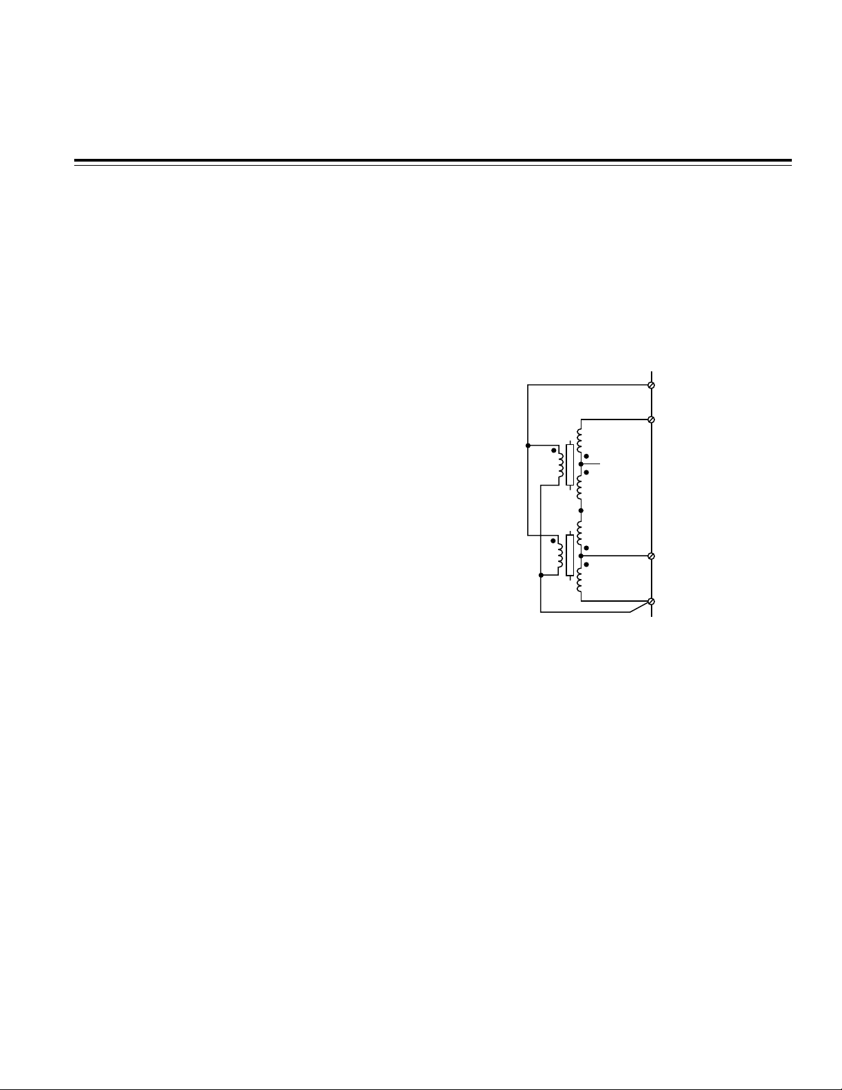
Figure 1. Additive LVDT Connections
+EXC
2
A – B (SIGNAL)
A
–EXC
3B17
In a gaging application where many measurements are
made, and thus many LVDTs are used, the cost for
a signal conditioner for each transducer can be high.
One Analog Devices’ 3B17 LVDT signal conditioner can
be configured to handle two inputs for both the differential and additive applications, thus cutting the signal conditioning costs in half. Figure 1 shows two LVDTs connected
together with the input to the signal conditioning being the
sum of both LVDTs. The LVDTs should have matched
gains. Both LVDTs will receive the same excitation
signal up to a maximum of 20 mA. The demodulation
synch signal internal to the signal conditioner is two
times the voltage at Pin 3 of the conditioner (labeled A)
minus the voltage at Pin 2 (labeled A – B). This signal
should not vary more than +50%. Numerically this
indicates:
|
V
| > |(
A – B
)1 + (
A – B
A
1
)2|
MODEL 3B17 LVDT INPUT SIGNAL CONDITIONING
MODULE
The 3B17 is a nonisolated signal conditioning module
for LVDT interfacing. It provides a programmable, very
stable, low distortion ac excitation voltage for the transducer and accepts a 20 mV rms to 5 V rms input signal
from the LVDT. All gain and span adjustments are accomplished with screwdriver attachments on the top of
the module. The interpretation of the LVDT output voltage is done with a synchronous demodulator. This demodulator converts the ac output of the LVDT into a dc
voltage. It automatically compensates for any phase
error between primary and secondaries of the LVDT,
and eliminates the need for a phase adjustment. It also
rejects any residual quadrature or null voltage providing
accurate, linear ±10 volt and 4 mA–20 mA outputs.
Page 2

AN-536
+EXC
A – B
–
B
+
+
A
–
–EXC
P2
V/I
I
SPAN
I
PROTECTED
PRECISION
P1
1
2
3
4
OSCILLATOR
INPUT
PROTECTION
PROTECTION
RANGING CARD
(IF USED)
AMP
V
SPAN
A + B
DEMOD
V
OUT
ZERO
JUMPERS
V
ZERO
OUTPUT
PROTECTION
3B17
I
OUT
I
OUT
RETURN
LOOP V+
LOOP COM
COM
V
OUT
+15V
PWR COM
–15V
1
R
2
L
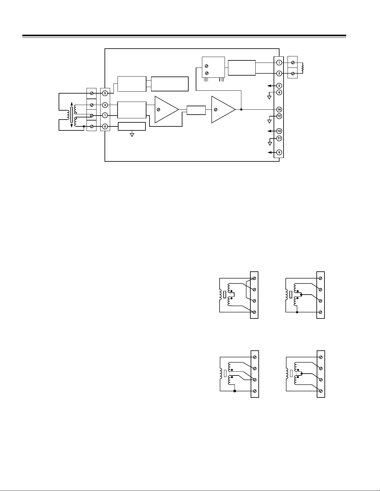
Figure 2. Block Diagram of Model 3B17
INSIDE THE 3B17
The 3B17 accepts inputs from 4-wire, 5-wire and 6-wire
LVDTs or RVDTs. A block diagram of Model 3B17 is
shown in Figure 2.
The 3B17 provides an ac excitation of 1 V rms to 5 V rms
at frequencies ranging from 1 kHz to 10 kHz on input
screw terminals 1 and 4. The ac excitation is limited to a
20 mA rms load; this sets a lower circuit primary imped-
ance of 50 Ω for a 1 V excitation and 250 Ω for a 5 V
excitation. If the primary impedance of the LVDT/RVDT
is below 50 Ω, the impedance of the LVDT/RVDT can be
increased by increasing the excitation frequency. Input
protection of up to 130 V rms is provided for the excitation and input circuitry. The signal is amplified to provide the high level voltage output.
The 3B17 is designed to compensate for error terms
typically found in LVDT or RVDT applications, such as
quadrature voltages (voltages that are 90° out-of-phase
to the output signal) and null voltages. Quadrature and
null voltages can appear at the differential output of the
LVDT/RVDT; they can be caused by interwinding capacitance and winding asymmetries or a fixed-phase shift
from the primary to the secondary of the LVDT/RVDT.
The two secondary windings are identified as A and B,
with the normal output being A – B. (Refer to Figure 1).
The 3B17 generates the function A + B (a voltage that is
in phase with the secondaries and nearly invariant with
the core replacement) by manipulating the A and A – B
outputs. Since A + B is much larger than the quadrature
voltage, A + B can drive the demodulator, eliminating
the need to manually trim the phase of the demodulator.
In addition, the 3B17 automatically rejects any residual
quadrature voltages.
You can adjust the voltage output over ±5 V from the
center setting of the LVDT/RVDT. After you adjust the
voltage output, you can independently adjust the 130 V
ac protected current output over a ±5% span range for
zero and span.
OTHER LVDT CONNECTIONS
A 6-wire LVDT is shown connected to the 3B17 in Figure
2. 4-wire and 5-wire connections are shown in Figures
3a, 3b, 4a and 4b.
1
2
3
4
1
2
3
4
a. b.
Figure 3. Four-Wire LVDT Connections
11
2
3
4
2
3
4
a. b.
Figure 4. Five-Wire LVDT Connections
–2–
Page 3

AN-536
USING THE 3B17 FOR DIFFERENTIAL COIL
CONDITIONING
The 3B17-D version of the 3B17 module can be used for
differential coil applications as shown in Figure 5. The
3B17-D is intolerant of a capacitive load across the excitation terminals that is greater than 100 pF. Any capacitor that is across the entire differential coil must be
removed.
1
+EXC
2
HI
3B17-D
3
LO
4
–EXC
Figure 5. Differential Coil Connection
USING NONSPECIFIED EXCITATION VOLTAGE AND
FREQUENCY
Whenever possible, the voltage and frequency of the
excitation provided by the 3B17 module should match
the voltage and frequency of the LVDT/RVDT specification. If this results in an excitation current of more than
20 mA rms load on the excitation pins of the 3B17, the
following procedure is recommended;
• Decrease the excitation voltage to 1 V rms. The 3B17
operates at gains of up to 230 (V
DC OUT/VRMS IN
), and
can support the increased gain demand;
• Increase the frequency to 10 kHz; this increases the
primary impedance. Keep in mind that the primary to
secondary phase shift changes, however, the internal
synchronization automatically compensates for any
change in phase shift. In addition, the linearity of the
LVDT/RVDT may change when operated at a different
frequency than specified. Consult the LVDT/RVDT
data sheet or manufacturer for more information.
E3306–5–4/98
–3–
PRINTED IN U.S.A.
 Loading...