AN-501
()(
π
=
(
)
(
π
=
One Technology Way • P.O. Box 9106 • Norwood, MA 02062-9106, U.S.A. • Tel: 781.329.4700 • Fax: 781.461.3113 • www.analog.com
APPLICATION NOTE
Aperture Uncertainty and ADC System Performance
by Brad Brannon and Allen Barlow
APERTURE UNCERTAINTY
Aperture uncertainty is a key ADC concern when performing
IF sampling. The terms aperture jitter and aperture uncertainty
are synonymous and are frequently interchanged in the
literature. Aperture uncertainty is the sample-to-sample
variation in the encoding process. It has three distinct effects on
system performance. First, it can increase system noise. Second,
it can contribute to the uncertainty in the actual phase of the
sampled signal itself giving rise to increases in error vector
magnitude. Third, it can heighten intersymbol interference
(ISI). However, in typical communications applications, an
aperture uncertainty that is sufficiently small to meet system
noise constraints results in negligible impact on phase
uncertainty and ISI. For example, consider the case of sampling
an IF of 250 MHz. At that speed, even 1 ps of aperture jitter can
limit any ADC’s SNR to only 56 dB, while for the same
conditions, the phase uncertainty error is only 0.09 degrees rms
based on a 4 ns period. This is quite acceptable even for a
demanding specification such as GSM. The focus of this
analysis is, therefore, on overall noise contribution due to
aperture uncertainty.
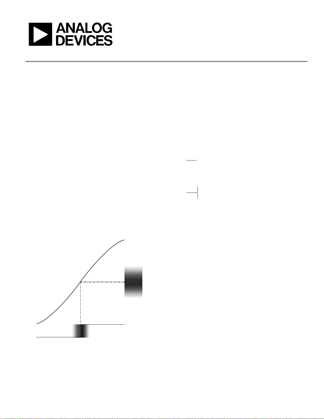
Figure 1 illustrates how an error in the sampling instant results
in an error in the sampled voltage. Mathematically, the
magnitude of the sampled voltage error is defined by the time
derivative of the signal function. Consider a sine wave input
signal
(1)
)
ftAtv
2sin
The derivative is
tdv
dt
The maximum error occurs when the cosine function equals 1,
that is, at t = 0.
)
dv
0
dt
max
We s e e fr o m
corresponding to the jitter dt. For conceptual clarity, if we
relabel dv as V
factors, we get
fA
π
2
=
Figure 1 that dv is the error in the sampled voltage
and dt as ta (aperture error) and rearrange the
err
(4)
ftAV
2
aerr
(2)
(
)
ftfA
ππ
2cos2=
(3)
ENCODE
dt
Figure 1. RMS Jitter vs. RMS Noise
ERROR VOLTAGE
dv
01399-001
Rev. A | Page 1 of 4
If t
is given as an rms value, the derived V
a
Although this is the error at maximum input slew and
represents an upper bound rather than a nominal, this simple
model proves surprisingly accurate and useful for estimating
the degradation in SNR as a function of sample clock jitter.
is also rms.
err
JITTER AND SNR
As Equation 4 indicates, the error in the sampled voltage
increases linearly with input frequency, so at high frequencies,
for example, in IF sampled receiver applications, clock purity
becomes extremely important. Sampling is a mixing operation:
the input signal is multiplied by a local oscillator or in this case,
a sampling clock. Because multiplication in time is convolution
in the frequency domain, the spectrum of the sample clock is
convolved with the spectrum of the input signal. Considering
that aperture uncertainty is wideband noise on the clock, it
shows up as wideband noise in the sampled spectrum, periodic
and repeated around the sample rate.

AN-501
W
A
Because ADC encode inputs have very high bandwidth, the
effects of clock input noise can extend out many times the
sample rate itself and alias back into the baseband of the
converter. Therefore, this wideband noise degrades the noise
floor performance of the ADC. Consider a sinusoidal input
signal of amplitude A. Utilizing Equation 4, the SNR for an
ADC limited by aperture uncertainty is
SNR
A
V
err
(5)
(
ft
π
2log20log20 −==
)
a
Equation 5 illustrates why systems that require high dynamic
range and high analog input frequencies also require a low jitter
encode source. For an analog input of 200 MHz and only
300 femtoseconds rms clock jitter, SNR is limited to only
68.5 dB, well below the level commonly achieved at lower
speeds by 12-bit converters. Note in Equation 5 that the jitter
limit of SNR is independent of the converter resolution. (For
the case just mentioned, a 14-bit converter would do no better.)
Aperture jitter is not always the performance limiter. Equation 6
shows its effect in superposition with other noise sources. The
first term in the brackets is the jitter from Equation 5. To that,
we must add terms for quantization noise, DNL, and thermal
noise. For other analytic purposes, each of these could be
broken out separately, but for simplicity in isolating the effect of
jitter, we combine them here in a single additional term.
2/1
2
⎡
2
()
tfSNR
2log20
π
⎢
⎢
⎣
+−=
a
⎤
1
ε
+
⎛
⎜
2
⎝
(6)
⎞
⎟
⎥
N
⎠
⎥
⎦
where:
f = analog input frequency.
t
= aperture uncertainty (jitter).
a
ε = “composite rms DNL” in LSBs, including thermal noise.
N = number of bits.
This simple equation provides considerable insight into the
noise performance of a data converter.
MEASURING SUBPICOSECOND JITTER
Aperture uncertainty is readily determined by examining SNR
without harmonics as a function of analog input frequency. Two
measurements are required for the calculation. The first
measurement is done at a sufficiently low analog input
frequency that the effects of aperture uncertainty are negligible.
Since jitter is negligible, Equation 6 can be simplified and
rearranged to solve for ε, the “composite DNL.”
−SNR
N
20
1102
−×=ε
(7)
Next, an FFT is done at high (IF) frequency. The high frequency
chosen should be as high as possible. Again, the SNR value
without harmonics is measured. This time jitter is a contributor
to noise and solving Equation 6 for t
2
SNR
−
10
⎞
20
⎟
⎟
⎠
π
2
ε
1
+
⎛
−
⎜
N
2
⎝
f
⎛
⎜
⎜
⎝
t
=
a
yields
a
2
⎞
⎟
⎠
(8)
where:
SNR = the high frequency SNR just measured
ε = the value determined in the low frequency measurement.
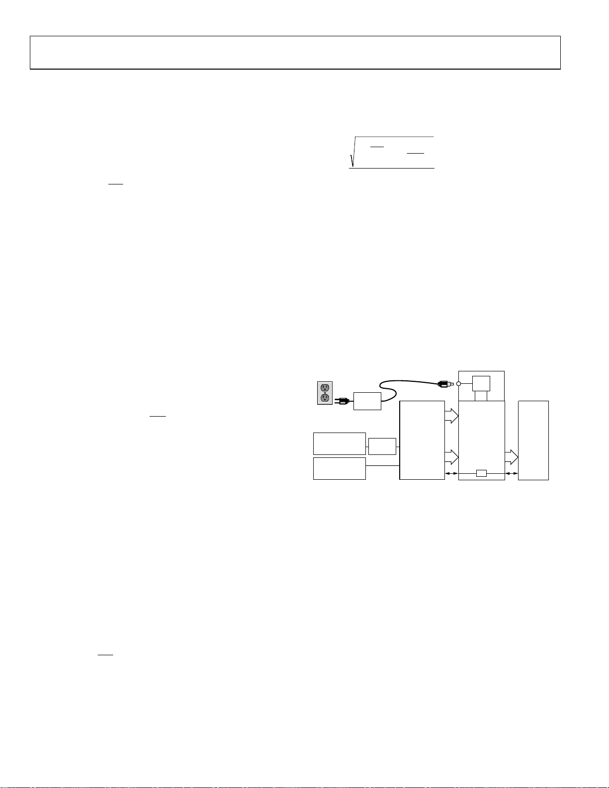
EXAMPLE: JITTER AND THE AD9246
The example shown here utilizes the AD9246 evaluation board,
a 14-bit, 125 MSPS ADC. An external clock oscillator such as a
Wenzel Sprinter or Ultra-Low Noise provides a suitable encode
source. A mainstream RF synthesizer from Rohde & Schwarz or
Agilent can be used for the analog source. Typically, these
generators have insufficient phase noise performance for use as
the encode source. For more information about configuring
Analog Devices evaluation boards, please consult the individual
product data sheet.
LL OUTLET
100V TO 240V AC
47Hz TO 63Hz
6V DC
PARALLEL
BOARD
PARALLEL
CHB
CMOS
OUTPUTS
CHA
CMOS
OUTPUTS
2A MAX
ROHDE & SCHWARZ,
SMHU,
2V p-p SIGNAL
SYNTHESIZER
ROHDE & SCHWARZ,
SMHU,
2V p-p SIGNAL
SYNTHESIZER
SWITCHING
POWER
SUPPLY
BAND-PASS
FILTER
EVALUATION
XFMR
INPUT
CLK
Figure 2. Aperture Uncertainty Measurement Setup with AD9246 Customer
Evaluation Board
Figure 3 is a 5 average, 64 K FFT of the AD9246 sampling a 2.3
MHz sine wave at 125 MSPS. Analog Devices’ ADC Analyzer
Software (
www.analog.com/fifo) collects and processes the data
to report SNR without harmonics. From the plots, the SNR is
72.05 dBFS.
3.3V
–+
VCC
GND
HSC-ADC-EVALB-DC
FIFO DATA
CAPTURE
BOARD
USB
CONNECTION
SPI
PC
RUNNING
ADC
ANALYZER
SPISPI
TM
01399-002
Here, SNR is the low frequency value just measured.
Rev. A | Page 2 of 4
 Loading...