Page 1

AN-414
a
ONE TECHNOLOGY WAY • P.O. BOX 9106
Low Cost, Low Power Devices for HDSL Applications
HDSL OVERVIEW
Applications
The proliferation of ISDN (Integrated Services Digital
Network) demonstrates the demand for high speed modems for transmission of data. HDSL (High Speed Digital
Subscriber Line) is a transmission scheme that fills the
gap between the 128 kbps ISDN and ADSL (Asynchronous Digital Subscriber Line). Chipsets already available
from Analog Devices support ADSL transmission of
video rate data into the home. Although HDSL cannot
support this data rate, like ADSL, HDSL will provide high
speed data transmission over existing twisted pair telephone lines. Unlike ADSL, HDSL transmits at the same
rate upstream and downstream. T1 rates (US) specifies
1.544 Mbps over one or two pairs of copper line while E1
rates (Eur) call for 2.048 Mbps. HDSL modems available
today support data transmission at these rates over two
pair of copper wire, with equal data rates on both pairs.
Single pair systems that can support the full data rate
provide the system architecture with a pair gain of two.
This has a more limited range and requires much more
sophisticated DSP. HDSL systems do not require that the
lines be matched; they can still transmit accurately with
stubs present on the transmission line.
•
NORWOOD, MASSACHUSETTS 02062-9106
by Ed Spence
HDSL modems available today support data transmission at these rates over two pair of copper, with equal
data rates on both pairs (i.e., 784 kbps on each pair for a
T1 link; 1168 kbps for E1, although a few systems use
three pairs at 768 kbps to carry an E1 rate).
A typical HDSL application might be the T1/E1 link between a cellular phone system basestation transceiver
and the basestation controller; as well as a high speed
modem for internet access and replacement for T1 lines.
Another, especially popular in developing countries, is
digital pair gain—increasing the number of users on a
single loop.
There is another acronym around: “MDSL” (moderate
speed) is a minor variation on HDSL; often half of a two
pair HDSL system, to deliver lower rates.
MODULATION METHOD
Data transmitted on HDSL lines are coded with 2B1Q
(2 Bits 1 Quaternary) coding. This PAM modulation
method groups data bits into 2 bits per symbol, with
each symbol represented by one of four power levels.
The symbol rate is therefore 1/2 the bit rate. A sample
2B1Q waveform is shown in Figure 1.
APPLICATION NOTE
617/329-4700
•
+3
+1
–1
–3
QUATS
BITS
TIME
–1
+310+111–300–300+111+310–300–101–101+111–101–300+310+310–101+1
01
Figure 1. Example of 2B1Q Quaternary Symbols
11
Page 2

BIT RATES
T1 rates specify 1.544 Mbps. This translates to a baud
rate of 784 kbaud (symbols/second). The baud rate is not
exactly a factor of 2 because of error correction bits
added to data. The error correction supports adaptive
equalization of the transmission line as well as 2nd order echo cancellation. Adaptive equalization is a DSP
process that continuously tunes the digital filters to
match conditions on the line. For two pair lines the symbols are transmitted over each twisted pair at equal
rates; therefore the line transceiver circuitry must support 1/2 the modem baud rate.
POWER CONSTRAINTS
The remote modem at the user site is line powered,
drawing power from the copper pair, making the power
consumption of the modem critical.
T1/E1 CHIPSETS:
PAIRGAIN
BROOKTREE
METALINK
TRANSCEIVER
AD9760
AD9762
AD768B
D/A
10–16 BITS
E1/T1
SYMBOL RATES
BLOCK DIAGRAM/ FUNCTIONS
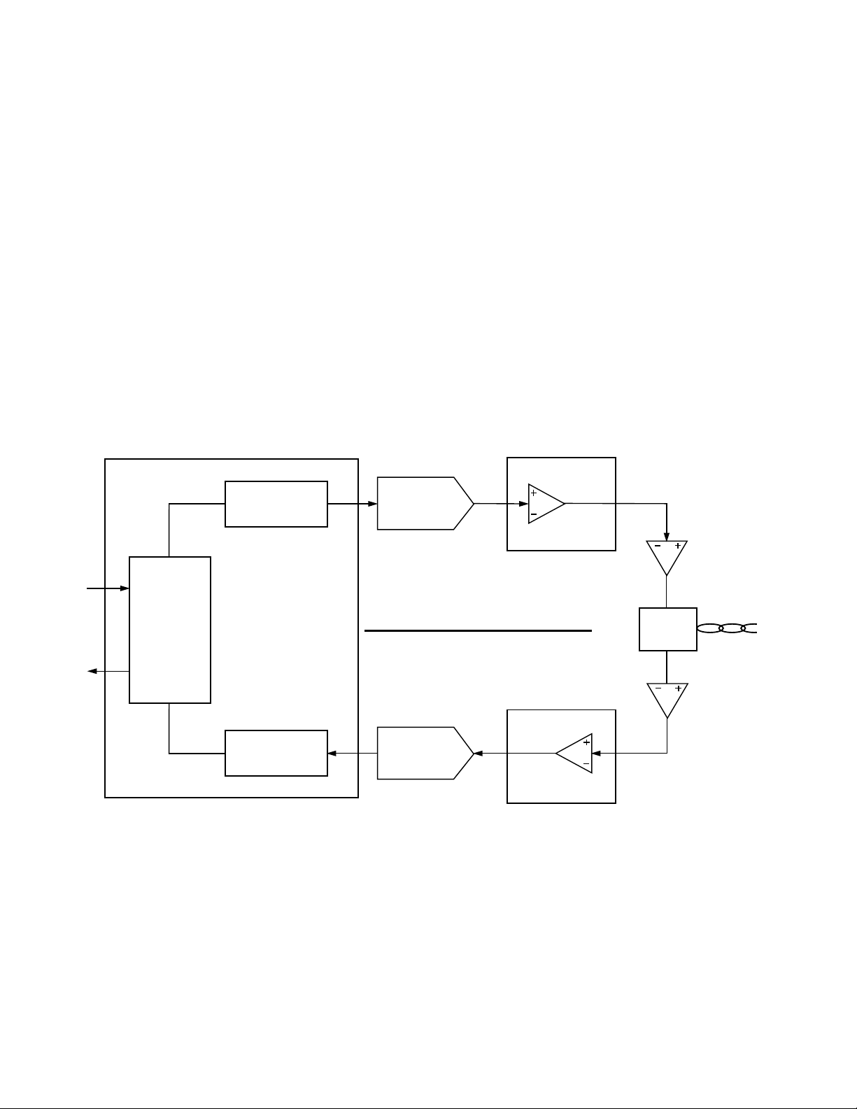
A functional block diagram of a generic HDSL modem is
shown in Figure 2. The interface to the twisted pair
is through a transformer “hybrid,” where an analog
front end (AFE) circuitry drives and receives the PAM
signal. Figure 3 shows the Analog Devices AD812 dual,
145 MHz operational amplifier used to drive the transformer differentially. The PAM signal is received from
the encoder and applied to both amplifiers of the AD812.
The dual configuration drives the signal differentially
across the primary, where the voltage is stepped up by a
factor of two on the twisted pair. This transmitted voltage is also sensed (divided down) and applied to one
side of a differential amplifier, 1/4 of an OP467, an Analog Devices quad, 28 MHz operational amplifier. The
OP467 amplifier is the first stage of a receiver block,
which receives the bipolar signal from the twisted pair
line on the other half of the difference amplifier configuration. This circuit essentially performs a 1st order echo
cancellation.
PULSE SHAPING
FILTER
AD8044
AD467
LINE DRIVER
T1/E1
T1/E1
FRAMER/
CHANNEL
UNIT
FUNCTIONS:
BIT PACKING
ECHO CANCELLATION
FRAMING
FILTERING
ADAPTIVE EQUALIZATION
CLOCK RECOVERY
TRANSCEIVER
Figure 2. HDSL Modem Block Diagram
AD7892
AD9221/3
A/D
12 BITS
TRANSMIT SIGNAL PATH
RECEIVE SIGNAL PATH
(0.6MSPS)
(1/3 MSPS)
ANTI ALIAS
FILTER
AD467
AD8044
AD8042
AD812
TO OTHER
TRANSCEIVER
XFMR
EXISTING
COPPER
PAIR
–2–
Page 3

2kΩ 3kΩ
4.7Ω
0.47µF
8
R6
232
V
IN
2kΩ 3kΩ
6
5
AD812
A1A
7
+5V
ATT
2718AF
93DJ39
1
4
V
OUT
0.001µF
A1 = AD812
DUAL OP AMP
–5V
4.7Ω
A1B
2
AD812
3
4
1kΩ
0.001µF
Figure 3.
1
0.47µF
912Ω
0.0027µF
2kΩ
2kΩ
2kΩ
10
2
9
34Ω
2kΩ
0.47µF
4
2
OP467
3
13
0.47µF
5
7
6
10Ω
R25
1
249Ω
10Ω
V
+5V
REC
–5V
For a single supply solution, the wide bandwidth, low
power AD8042, dual 160 MHz and the AD8044 quad,
150 MHz op amps are well suited for this application.
The AD8042’s low power of 5.2 mA/A and the AD8044’s
3.25 mA/A provide a low power solution for line powered modems. Another single supply ADC solution that
has been designed into two pair modems is the AD7892.
This low cost, 12b, 600 kSPS ADC operates on 60 mW.
The received signal can then be filtered by an active
filter (i.e., 4th order Sallen-Key filter). The pole is set at
the baud rate to prevent aliasing in the ADC. Two more
of the high speed op amps included in the OP467 can be
used to perform this filter function. A good choice
of ADC is a low power, single supply AD9221, a 12b,
1.25 MSPS ADC that digitizes the received PAM
signal for further processing. The AD9221 consumes
only 50 mW of power at this sample rate, and can process a rail-to-rail +5 V input signal. The 1.25 MSPS minimum sample rate makes it fast enough for single pair T1
application, since the ADC must be capable of sampling
at the symbol rate.
For E1 systems, a drop in replacement for the AD9221,
the AD9223 can be used instead. The AD9223 is a 12b,
3 MSPS solution which requires only 100 mW of power.
The driving characteristics of this ADC input are exactly
the same as the AD9221. The fact that both ADCs are
drop in replacements for each other gives the system
designer added flexibility to adjust power consumption
to meet performance requirements of the receiver system. The ADCs are low cost and easy to use, and the
input range is selected by a resistor. The input can
accept rail to rail voltage inputs to maximize the
dynamic range. Both ADCs are due for release in 2Q96.
A low resolution DAC (e.g., 7 bit) is also required for
timing recovery purposes to tune the VCXO.
FUTURE DEVELOPMENTS
ADI is also developing a single chip analog front end (integrating ADC, DAC, PGA, filters, timing recovery DAC
and driver), which will be sampling late this year. There
will be two versions of this part, one suited to two/three
pair applications and one for the faster single pair applications. This may include a few other useful features or
nice “tweaks.”
We will also be developing some digital devices, to offer
a complete solution.
–3–
Page 4

SUMMARY
A low cost, low power transceiver solution for an HDSL
modem can be implemented with minimum components. The AD812 and OP467 provide a flexible solution
for high speed transceiver applications. The AD9221 and
AD9223 are pin compatible replacements for the
AD9220, a popular 12b, 10 MSPS single supply ADC
available now from ADI.
For a single supply solution, the wide bandwidth, low
power AD8042, dual 160 MHz and the AD8044 quad,
150 MHz op amps are well suited for this application.
We are committed to this market, with excellent discrete
solutions today and plans to help customers with integration in future generations.
REFERENCES
Bellcore TA-NWT-001210, Issue 1, October 1991, “Generic
Requirements for High-Bit-Rate Digital Subscriber Lines.”
E2124–6–4/96
–4–
PRINTED IN U.S.A.
 Loading...