

Page 1
AN-411
6
8
9
10
2
3
5
0.022µF
C2
ADXL05
PRE-AMP
0.022µF
COM
C1
C1
V
PR
+1.8V
BUFFER
AMP
+5VDC
C3
0.1µF
V
ACCEL
R1
R2
C5
V
IN–
R3
4
1
1
2
4
5
6
7
8
R
T
R
T
LOGIC
COM
F
OUT
R5
1kΩ to 10kΩ
FREQUENCY
OUTPUT
+V
S
+V
S
C4
0.1µF
C
T
C
T
C
T
–V
S
+V
IN
DRIVER
OSC
AD654
3
0g FREQ SF CTR1 R2 R3
Hz Hz/
g
µF kΩ kΩ kΩ
10 10 10 14.7 464 182
100 10 1 40.2 127 49.9
100 100 1 14.7 464 182
1000 10 0.1 133 42.2 16.5
1000 100 0.1 40.2 127 49.9
1000 1000 0.1 14.7 464 182
10,000 10 0.01 1370 43.2 16.9
10,000 100 0.01 137 43.2 16.9
10,000 1000 0.01 40.2 127 49.9
100,000 10 0.001 137 0.43 0.169
100,000 100 0.001 137 4.32 1.69
100,000 1000 0.001 137 43.2 16.9
DESIGN EQUATIONS
0.25
RT C
T
0g FREQUENCY =
R2 FOR A +2.5V 0
g
LEVEL = 2.57 R3
SCALE FACTOR (Hz/
g
) = =
∆ FREQ
g
200 R3
1000 R1 RT C
T
3dB ACCELERATION BW =
1
2π R3 C5
IN4733
R
S
+V
S
+5VDC TO
PIN 1
ADXL05
+V
S
+VSR
S
+12V 432Ω
+9V 249Ω
a
ONE TECHNOLOGY WAY • P.O. BOX 9106
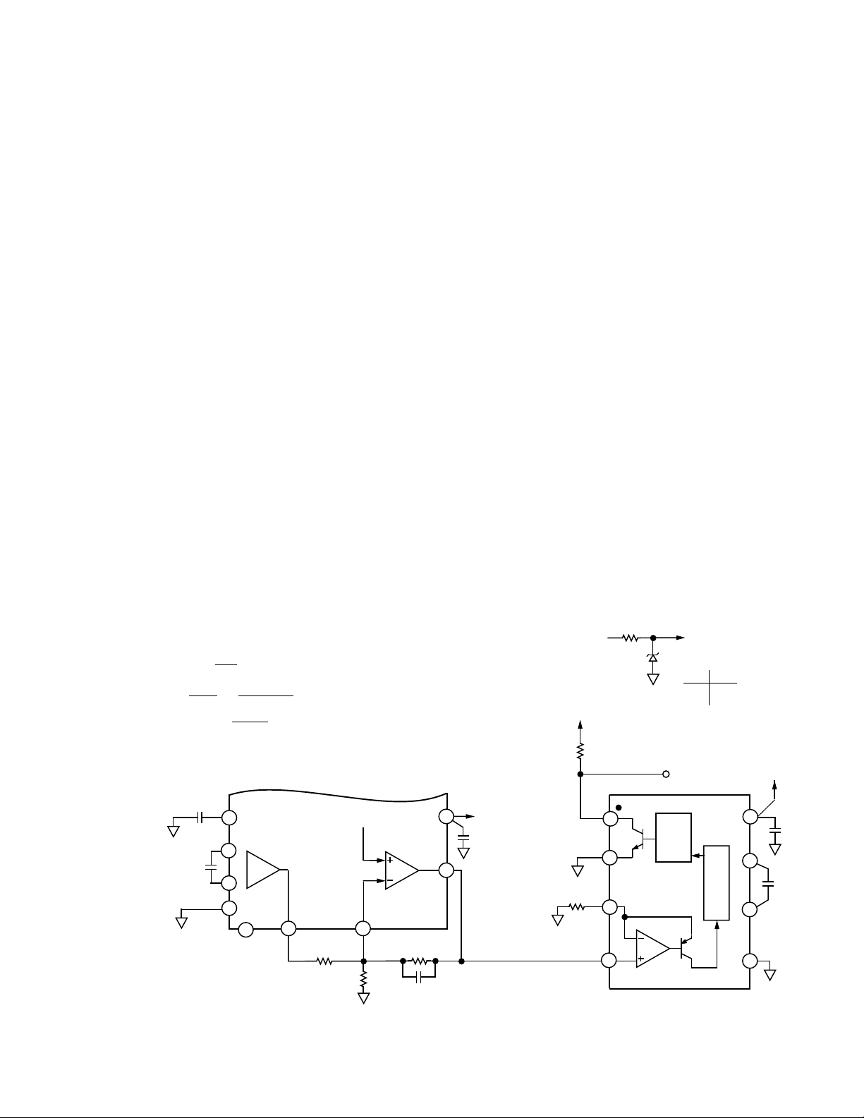
Acceleration to Frequency Circuits
by Charles Kitchin, Dave Quinn, and Steve Sherman
INTRODUCTION
Low cost monolithic accelerometers may be paired with
a circuit whose output changes with frequency (V/F) to
provide a TTL level frequency output. A microprocessor
can be easily programmed to read this signal and
directly compute the applied acceleration, and the output of a V/F circuit can be sent down a long transmission
line and still be reliably recovered at the other end.
A High Performance Acceleration-to-Frequency Circuit
A circuit whose output frequency varies directly with
applied acceleration is shown in Figure 1. The circuit
operates from a single +9 V or +12 V power supply.
•
NORWOOD, MASSACHUSETTS 02062-9106
APPLICATION NOTE
617/329-4700
•
An ADXL05, ±5 g accelerometer directly converts any
applied acceleration into an analog output voltage
which then controls the output frequency of an AD654
low cost voltage-to-frequency converter IC. The frequency output appears at Pin 1 of the AD654. Total chip
cost for this circuit is approximately $20.00 (in 1000s).
The voltage output at Pin 8 of the ADXL05 is +2.5 volts
with no acceleration and varies 200 mV above or below
that value for each 1
acceleration.
g
(positive or negative) of applied
Figure 1. A High Performance Acceleration-to-Frequency Circuit
Page 2
The output scale factor of the accelerometer (at Pin 9) is
set by the resistors R3 & R1 of the on-chip buffer amplifier. Resistor R2 is used to change the 0
g
output level to
a convenient +2.5 V (which provides the maximum output voltage swing). Capacitor C5 and Resistor R3 form a
low-pass filter which improves the circuit’s signal-tonoise ratio.
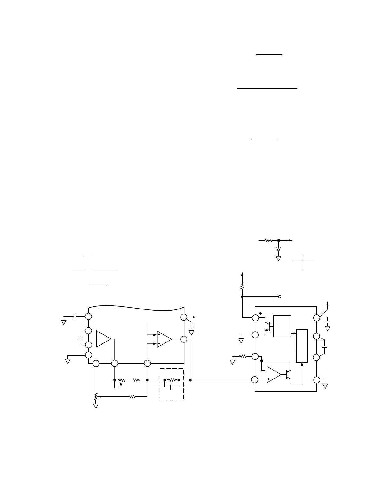
Figure 2 shows the same circuit modified for use with
the ADXL50, a ±50
g
accelerometer. The accelerometer’s
3 dB bandwidth is again set by R3 & C5. In Figure 2, both
a zero
g
offset and a scale factor trim potentiometer
have been added to allow the user to adjust the circuit to
extremely high accuracy; trim potentiometers may also
be added to the circuit of Figure 1. R1a should be approximately 50% the value of R1b (for a ±20% trim
range). Note: for the best mechanical stability the trim
potentiometers should be measured (after calibration is
complete) and replaced with 1% resistors.
Design example: Circuit of Figure 2
Design example: Wanted . . . 0
Scale Factor = 100 Hz/
g
, BW = 200 Hz.
g
frequency = 10 kHz,
A 50 g signal will cause a frequency variation of 5 kHz.
Therefore:
F
for
±50
OUT
Let
C
gs = 10 kHz ± 5 kHz = 5 kHz – 15 kHz
= 0.01 µF, then for a 0 g frequency of 10 kHz:
T
R
0.25
=
T
kHz C
10
=2.5kΩ
T
Let R3 = 49.9 kΩ, for a scale factor of 100 Hz/g:
mV/g×R
100
19
Hz/g
10,000
R
1=
3
RTC
=52.7kΩ
T
For R1, use a 42.2 kΩ fixed resistor & a 20 kΩ trim
potentiometer.
For a 200 Hz bandwidth:
C
5 =
1
2π 200
R
3
= 0.016 µ
F
The accelerometer may be self-calibrated by using the
Earth’s gravity. With the accelerometer’s tab pointed
90° to the vertical (i.e., to either side), the accelerometer
will measure 0
g
, allowing the 0 g offset to be adjusted.
With the accelerometer’s tab pointing down, its output
at Pin 9 will correspond to +1
rotated 180° it will then measure –1
g
. If the accelerometer is
g
. The 2 g difference
in the readings can then be used to set the circuit’s over-
DESIGN EQUATIONS
∆ FREQ
g
0.022µF
COM
OPTIONAL
0
C2
C1
C1
g
LEVEL
0.25
RT C
+3.4V
TRIM
0g FREQUENCY =
SCALE FACTOR (Hz/g) = =
3dB ACCELERATION BW =
0.022µF
T
1000 R1 RT C
2π R3 C5
4
2
3
5
6
REF
19 R3
1
R4
50kΩ
TRIM
T
ADXL50
PRE-AMP
V
PR
8
SF
0g FREQ SF CTR1a R1b R2 R3
Hz Hz/
10 10 10 5 12.1 100 2MΩ
100 10 1 10 34.8 100 499
100 100 1 5 12.1 100 2MΩ
1000 10 0.1 50 107 100 165
1000 100 0.1 10 34.8 100 499
1000 1000 0.1 5 12.1 100 2MΩ
10,000 10 0.01 500 1MΩ 100 169
10,000 100 0.01 50 107 100 169
10,000 1000 0.01 10 34.8 100 499
100,000 10 0.001 50 107 100 1.69
100,000 100 0.001 50 107 100 16.9
100,000 1000 0.001 50 107 100 169
R1a
100kΩ
R2
R1b
+1.8V
10
g
µF kΩ kΩ kΩ kΩ
1
BUFFER
AMP
9
V
IN–
R3
R2
C5
V
LOW-PASS
FILTERING
+5VDC
C3
0.1µF
ACCEL
+V
S
R5
1kΩ to 10kΩ
F
OUT
LOGIC
COM
R
T
5.9kΩ
+V
R
S
+V
S
IN4733
1
2
R
IN
AD654
T
3
4
FREQUENCY
OUTPUT
DRIVER
+5VDC TO
PIN 1
ADXL50
+V
SRS
+12V 348Ω
+9V 200Ω
OSC
+V
S
+V
S
8
C4
0.1µF
C
T
7
C
T
0.1µF
6
C
T
–V
S
5
Figure 2. A ±50 g Acceleration-to-Frequency Circuit
–2–
Page 3

all scale factor. The 0 g& full-scale frequency adjustments should be repeated a couple of times to get the
highest accuracy.
An Accelerometer Tilt Sensor with a Frequency Output
Figure 3 shows how an ADXL05 accelerometer can be
connected to a low cost CMOS 555 timer to provide a
frequency output. The component values indicated were
selected for a ±1
g
tilt application.
The nominal 200 mV/g output of the accelerometer
appears at Pin 8 and is gained-up by a factor of 2 to a
400 mV/
g
level by the onboard buffer amplifier. The 0
g
bias level at Pin 9 is approximately 1.8 V. Capacitor C4
and Resistor R3 form a 16 Hz low-pass filter to lower
noise and improve the measurement resolution.
The CMOS 555 operates as a voltage controlled oscillator where R5, R6, and C5 set the nominal operating
frequency. Resistors R5 & R6 were chosen to give an
approximate 50% duty cycle with a +1.8 V (0
g
) input signal applied to Pin 5 of the 555. To prevent any change in
frequency due to supply variations, the 555 operates
from the accelerometer’s +3.4 V reference rather than
directly off the +5 V supply.
The output frequency of this circuit is determined by the
charge and discharge times set by R5, R6, and C5.
Using the circuit and component values shown in Figure
3, the output scale factor at Pin 9 of the accelerometer
will be ±400 mV/
g
so the voltage output will be +1.8 V ±
0.4 V. The output scale factor at Pin 3 of the 555 will
be approximately 16,500 Hz ± 2,600 Hz per
g
. Figure 4
shows the circuit’s output frequency vs. the voltage
occurring at Pin 5 of the 555.
Frequency stability of this circuit is quite good. With a
15.5 kHz 0
g
frequency, the measured 0 g frequency drift
over the 0°C to +70°C commercial temperature range
was 5 Hz/°C which is 0.03%/°C. The change in frequency
vs. supply voltage is less than 10 Hz with a +5.0 volt to
+9.0 volt supply range.
25000
20000
15000
10000
FREQ OUTPUT – Hz
5000
0
31
22.5
V
IN
1.5
0.022µF
0.022µF
C2
C1
C1
COM
4
2
5
3
ADXL05
PRE-AMP
V
PR
8
6
+3.4V
REF
V
PR
49.9kΩ
THE CHARGE TIME, TC, IS EQUAL TO:
= – (R5 + R6) C5 ( LN (1 – (VIN / 3.4V)) – LN (1 – (VIN / 6.8V)))
T
C
THE DISCHARGE TIME, T
= 0.69 R6 C5
T
D
THE FREQUENCY OUTPUT IS EQUAL TO:
FREQUENCY = 1/(T
R1
+ TD)
C
1.8V
10
, IS EQUAL TO:
D
Figure 4. Frequency Output vs. Voltage Input for the
Circuit of Figure 3
0.01µF
0.1µF
+5V
4, 8
5
555CP
2, 6
3
1
10kΩ
7
100kΩ
FREQUENCY
OUTPUT TO µP
R5
R6
C5
510pF
1
BUFFER
AMP
9
V
OUT
V
IN
R3
100kΩ
C4
0.1µF
10Ω
Figure 3. A Low Cost Accelerometer Tilt Sensor with a Frequency Output
–3–
Page 4

E2093a–6–4/96
–4–
PRINTED IN U.S.A.
 Loading...