

Page 1

AN-408
a
ONE TECHNOLOGY WAY • P.O. BOX 9106
AC Motor Control Using the ADMC200 Coprocessor
INTRODUCTION
This document describes the design of an ac motor control system using the ADSP-2115 digital signal processor (DSP) and the ADMC200 motion coprocessor. The
architecture illustrated in this application note can be
utilized for a number of systems, and was chosen for
illustration purposes only. The purpose of the document
is to demonstrate the use of the ADMC200 in the digital
implementation of a high speed motor control system.
The document starts with a system hardware description that illustrates the hardware simplification when using the ADMC200 and ADSP-2115. A typical control
scheme is described to demonstrate the ADMC200 features. A control algorithm is produced to match the described control scheme. The DSP control software is
presented in both pseudo code and in DSP assembly
code. This code demonstrates how the ADMC200 functions can be closely integrated into the control algorithm. Timing information is also presented which
shows how the shaft torque functions could be implemented in less than 20 µs.
SYSTEM HARDWARE
The complete system consists of a permanent magnet
ac servo motor with a shaft mounted resolver, a three
phase power inverter, and the motor control circuit. The
primary ICs in the control circuit are the ADSP-2115, the
ADMC200, and the AD2S90 resolver-to-digital converter
(RDC). The DSP is the shaft control processor and carries
out all the motion control and torque current loop functions. The ADMC200 is the interface between the DSP
and the inverter, and in addition provides the vector
•
NORWOOD, MASSACHUSETTS 02062-9106
by Aengus Murray and Paul Kettle
APPLICATION NOTE
617/329-4700
•
transformation functions required for ac motor control.
The interface to the host controller can be either via the
DSP data and address bus or via the serial port.
The motion control software is stored on an external
8-bit EPROM and is automatically loaded into the DSP’s
1K words of internal program RAM on power-up. Each
of the 24-bit program words is stored on the EPROM in a
4-byte segment. The DSP boot firmware copies the program from the EPROM to the internal RAM in the correct
order to rebuild the 24-bit wide program memory. This
arrangement limits the external EPROM requirement to
just a single slow memory device.
It is possible to switch between eight pages of program
memory RAM stored in a 32K EPROM. For example, the
first boot page could contain the programs which will
initialize all data variables (look up tables, etc.), configure the ADMC200 registers (setup PWM registers, etc.),
and perform self-diagnostic functions. While the second
page can contain the motion control algorithms which
are loaded at the end of the initialization phase.
The ADMC200 device can be connected directly to the
DSP data and address busses, as described in detail in
Appendix C. The internal registers can be written to in
the same way as data RAM placed in the low memory
address space. The shaft control algorithm can be timed
through the ADMC200 CONVST pin or via the interrupt
pin on the DSP.
Page 2
8K X 8
EPROM
(BOOT)
ADSP-2115
IRQ
ADDR
ADMC200
CONTROL
SEQUENCER
PARK
CLARKE
CENTER
BASED
PWM
t
A
t
C
3 PHASE
INVERTER
PM AC
MOTOR
DATA
CONTROL
SP1 SP0
HOST
REGISTERS
Figure 1. Motion Control Hardware
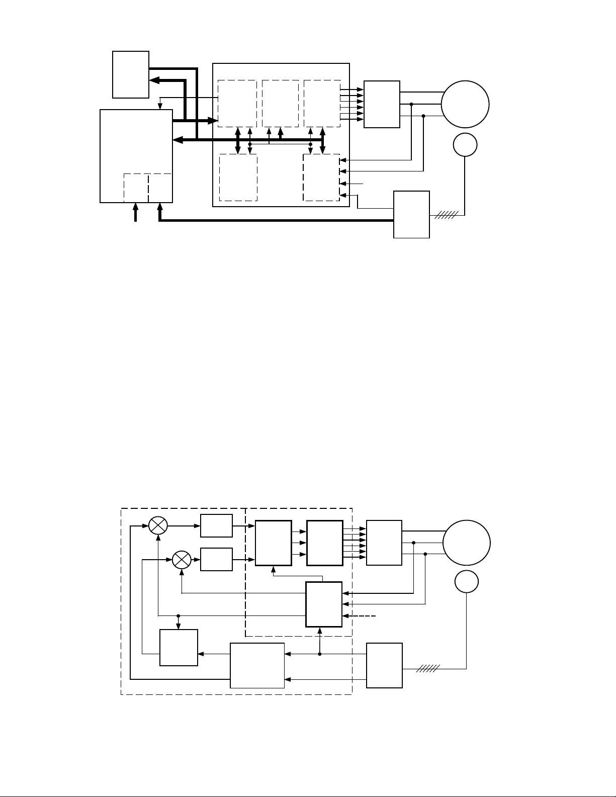
THE CONTROL SYSTEM
Figure 2 below illustrates a field oriented control
scheme for a permanent magnet synchronous motor.
The outer position and velocity loop calculates the
torque demand which is the input I
current loops. At speeds less than the base speed, the I
* reference for the
q
d
reference current will be zero. If an extended constant
power speed range is required, the field control scheme
can introduce some field weakening by setting a negative I
* value as a function of the motor speed.
d
*Reference input to controller.
I
4 CH SS
11–BIT
ADC
B
I
C
V
BUS
RESOLVER
ω
θ
AD2S90
The analog-to-digital converter (ADC) block within the
ADMC200 samples the motor currents; the vector transformation block performs a reverse Clarke and Park vector transformation on these ac current waveforms,
mapping them into equivalent direct and quadrature
*
current components within a rotating reference frame (I
d
Iq). A current loop control algorithm implemented on the
DSP calculates desired V
and Vq voltages for the motor.
d
Finally the ADMC200 forward vector transformation
block performs a forward Park and Clarke transformation, mapping these direct and quadrature motor voltages into ac voltages within the stator reference frame.
The DSP scales and then write these results to the PWM
block of the ADMC200.
ADSP-2115
–
+
–
FIELD
Id*
CONTROL
*
REFERENCE INPUT TO CONTROLLER
I_CONT
I_CONT
+
ω
Iq*
Figure 2. Motion Control System
V
q
V
d
I
d
I
q
POSITION
VELOCITY
CONTROL
AND
PARK
CLARKE
ADMC200
V
A
V
B
–1
V
C
–2–
PWM
CLARKE
PARK
θ
ω
t
A
3 PHASE
INVERTER
t
C
I
B
I
–1
C
= –IB –I
I
C
A
RDC
PM AC
MOTOR
RESOLVER
Page 3

CONTROL ALGORITHM
An outline of the control algorithm, based on the
scheme in Figure 2, is given in Table I. The functions in
bold are implemented on the ADMC200 coprocessor.
The scheduling of the control algorithm is synchronized
with the ADC interrupt service routine. In this application the ADC will generate an interrupt at a rate of
10 kHz. The torque control loop is realized at this frequency, while the motion loop is scheduled every fourth
ADC sample. The motion control loop can be segregated
into a
posterior
a priori
portion is executed during the first three time
slices while the
and
a priori
posterior
measurement portions. The
portion is executed in the forth
interval. The basic torque loop functions can be carried
out in less than 20 µs; this leaves the remaining 80% of
the time for the motion control loop and other functions.
The code required takes up less than 10% of the available 1K of internal program RAM.
Table I. Control Algorithm Outline
inputs ADMC200 Motion_Control out ADMC200
write register functions read register
Read_RDC ω ADCAUX
ρ
ω position_velocity_loop Iq*
ω Field_control I
* = 0 for ω < ω
(I
d
base
)
*
d
inputs ADMC200 Torque_control out ADMC200
write register functions register
Sample_phase_ currents I
I
b
I
c
PHIP2/VQ Clarke_Park
PHIP3 I
–1
ρ RHO (Ia = –Ib –Ic) I
I
q
I_control_q V
b
I
c
I
d
q
a
q
ADCV
ADCW
ID/PHV1/VX
IQ/PHV2
IX/PHV3
Iq*
ω
I
d
I_control_d V
d
Id*
ω
V
q
V
d
PHIP1/VD Park _ Clarke
PHIP2/VQ V
ρ RHOP V
V
a
V
b
V
c
T
a
T
b
T
c
PWMCHA PWM_out
PWMCHB
PWMCHC
PWM_scale T
–1
V
a
b
c
a
T
b
T
c
ID/PHV1
IQ/PHV2
IX/PHV3
–3–
Page 4

TORQUE_LOOP FUNCTIONS
A more detailed explanation of the torque control loop
is given in Table II. In this example the ADC sample rate
is tied to the PWM frequency by connecting the
PWMSYNC pin to the CONVST pin. All four channels are
converted in sequence, and the completion of the conversion process will be signaled by an interrupt to the
DSP, which initiates the Torque_loop. The control inputs
to this loop are the reference currents I
* (Id_ref) , Iq*
d
(Iq_ref) derived from the motion control loops. The measured inputs are two motor phase currents (I
, IC) and
B
the shaft angle ρ (rho). The outputs are six deadtime
compensated PWM signals for the inverter.
Only two current values are measured by the ADC since
the third phase is derived by the ADMC200 vector transformation block. The reverse vector transformation produces Id and Iq currents in the rotor reference frame.
The reverse Clarke and Park vector transformation block
executes in 37 clock cycles; the block interrupts the processor on completion. While the vector rotation has
been performed, the computation resources of the DSP
are thus free to perform other tasks such as overcurrent
detection or velocity signal conditioning. The current
loops are based on a machine back emf model with a PI
error loop, as outlined in Appendix B.
The winding resistance drops (IRq = I
q
*.R
stator
) are
precalculated by the motion control loop. The current
loop outputs, the Vd and Vq voltages, are fed to the
PARK block. When the shaft angle is loaded into the forward angle register (RHOP), the forward PARK transformation produces the three motor phase voltages.
The phase voltages can be scaled as a function of the
bus voltage and the PWM period. Deadtime compensation is implemented by adding/subtracting the deadtime
to/from the PWM zero offset time depending on the
phase current polarity. The DSP writes the three PWM
on time duty cycles to the PWM input register. The PWM
output registers are latched with the new duty cycle information at the beginning of the next PWM period. The
updated PWM duty cycle data is only latched if all three
of the input registers have been updated.
Sample code for some of these functions is given in
Appendix A. Two sets of circular arrays are used for the
phase currents and phase voltages. The ADMC200 registers are memory mapped to the data memory address
bus and so are read as data variables. The wait states for
the ADMC200 access are defined in the ADSP-2115 data
memory wait state control register. The use of indirect
addressing in the PWM_scale routine allows the use of
the simultaneous multiply and memory read function.
–4–
Page 5

Table II. Torque Loop Algorithm
Start_torque_loop wait for ADC interrupt elapsed
time
Read_ currents: ADC_int:
read Iph(2) from ADMC200: ADCV
read Iph(3) from ADMC200: ADCW 1.1 µs
load PARK registers write Iph(2) to ADMC200: PHIP2
for stator to rotor write Iph(3) to ADMC200: PHIP3
transformation write ρ to ADMC200: RHO
Clarke_Park
–1
meanwhile check for over current
wait for RPARK interrupt 5.1 µs
RPARK_int:
read PARK registers read Id from ADMC200: ID
read Iq from ADMC200: IQ
read Iph(1) from ADMC200: IX 5.9 µs
I_control_d DId_n1 = Id_ref - Id
error driven PI loop DVd_n1 = DVd_n + KPd*(DId_n1-KId*DId_n)
(save DVq_n and DIq_n DVd_n = DVd_n1
values) DId_n = DId_n1
+machine equations Vd = DVd_n1 + (L
)*velocity
S.Iq
+ [IRd=Id*.RS] 7.8 µs
I_control_q: DIq_n1 = Iq_ref - Iq
error driven PI loop DVq_n1 = DVq_n + KPq*(DIq_n1-KIq*DIq_n)
(save DVq_n and DIq_n DVq_n = DVq_n1
values) DIq_n = DIq_n1
+machine equations Vq= DVq_n1 + (K
E+LS.Id
)*velocity
+ [IRq=Iq*.RS] 9.6 µs
load PARK registers write Vq to ADMC200 VQ;
for rotor to stator write Vd to ADMC200: VD;
transformation write ρ to ADMC200: RHOP; 9.9 µs
Park_Clarke
–1
meanwhile do some velocity filtering
wait for FPARK interrupt 13.9 µs
read PARK registers FPARK_int:
read Vph(1) from ADMC200: PHV1
read Vph(2) from ADMC200: PHV2 14.8 µs
read Vph(3) from ADMC200: PHV3
PWM_out for I = 1,3
deadtime adjustment T0 = TPWM/2 + TPD
reverse for -ve Iph IF Iph(I) LT 0 T0 = TPWM/2 - TPD
calculate PWM times T(I) = T0 + VSCALE*Vph(I)
write to registers write T(I) to PWMCH(I)_ADMC200
end_for_loop 18.0 µs
–5–
Page 6

APPENDIX A: ASSEMBLY CODE SEGMENT FOR TORQUE LOOP
Read_ currents: ADC_int:
i3=^I_ph; {pointers for I_ph CIRC array}
Read ADC registers m1=1;
and write to PARK input l3=3;
registers ax0=dm(ADCV); {Read Iph(2) from ADCV_ADMC200}
dm(i3,m1)=ax0;
dm(PHIP1_VD)=ax0; {write Iph(2) to PHIP1_ADMC200}
ax1=dm(ADCW); {Read Iph(3) from ADCW_ADMC200}
dm(i3,m1)=ax1;
dm(PHIP2_VQ)=ax1;
ay0=dm(theta) {write theta to RHO_ADMC200:}
dm(RHO)=ay0 {start RPARK by writing to ADMC200}
i7=^error_int {error if next call takes > 37 cycles }
RPARK starts: call over_current {check for over current during PARK}
Clarke_Park
–1
i7=^RPARK_int; {interrupt vector set to RPARK }
rti:
Read PARK output RPARK_int:
registers including ay0=dm(IX_PHV3); {Read Iph(1) from ADCW_ADMC200}
derived third phase dm(i3,m1)=ay0;
current value. i0=^Ids; {pointer for Id and Iq}
l0=2;
set up pointers for ay0=dm(ID_PHV1); {Read Ids from ID_ADMC200}
current loop call dm(i0,m1)=ay0;
ax0=dm(IQ_PHV2); {Read Iqs from IQ_ADMC200}
dm(i0,m1)=ay0;
i4=^Id_ref;
m4=1;
l4=0;
i1=^DId_n
l1=2;
call I_control {current loop for Id return Vd in mr1}
dm(PHIP1_VD)=mr1; {write Vd to VD_ADMC200}
i1=^DIq_n;
i4=^Iq_ref;
modify(i0,m1); {i0 now points to Iq}
call I_control {current loop for Iq return Vq in mr1}
FPARK starts: dm(PHIP2_VQ)=mr1; {write Vq to VQ_ADMC200} ax0=dm(theta)
Park_Clarke
–1
dm(RHOP)=ax0; {write theta to RHO_ADMC200: start FPARK}
i7=^error_int; {error interrupt vector for > 37 cycles}
call ADC_filters;
i7=^FPARK_int; {store vector for park interrupt}
rti;
FPARK_int:
set up pointers i2=^V_ph; {pointers for V_ph}
for Vph m2=1;
l2=3;
Read PARK output ax0=dm(PHV1_VD); {Read Va from PHV1_ADMC200}
registers dm(i3,m3)=ax0;
ax0=dm(PHV2_VQ); {Read Vb from PHV2_ADMC200}
–6–
Page 7

dm(i3,m3)=ax0;
ax0=dm(PHV3); {Read Vc from PHV3_ADMC200}
dm(i3,m3)=ax0;
i1=^PWMTCHA; {pointers for pwmtcha_ADMC200}
m1=1;
PWM_out l1=1;
ay1=pwmtdt; {dead time compensation}
including: ax1=pwmtm_0; {pwmtm/2}
deadtime adjustment my0=dm(pwm_sc); {pwm scale factor}
mr0=0;
cntr=3;
do pwmout until ce ;
ar=ax1+ay1, ax0=dm(i3,m3); {t0 incl +tdt adjust}
af=pass ax0; {check current polarity}
if lt ar = ax1-ay1; {if -i then -tdt adjust}
mr1=ar; load adjusted t0}
mx0=dm(i2,m2); {v_ph}
mr=mr+mx0*my0(ss);
{ton=t0+(+/-tdt)+v_ph*(t0/vbus) }
pwmout:
dm(i1,m1)=mr1; {write to pwmtchx_ADMC200 }
call motion_control {run position and velocity in remaining time}
rti;
current_loop(13 ops) {
PI error driven loop. af = DIq_n1 = Iq_ref - Iq
mr = int = DIq_n *KIq
ar = sum = Diq_n1 + int
mr = DVq_n1 = DVq_n+(sum)*KPq PI part
ar = Vq_sum = DVq_n1 + IRq
mf = PHI = KEq+Id*Ls
mr = Vq = Vq_sum + velocity*PHI machine equations
}
I_control:
ax0=dm(i0,m1), ay0=pm(i4,m4); {ax0=Iq ay0=Iq_ref }
Iq error af=ay0-ax0, mx0=dm(i1,m1), my0=pm(i4,m4); {mx0=DIq_n, my0=KIq}
mr=mx0*my0(ss), my0=pm(i4,m4); {mx0=KPq}
integral part: ar = mr1+af, mr1=dm(i1,m1); {mr1=DVq_n}
proportional part: mr=mr+ar*my0(ss), ay0= pm(i4,m4); {ay0=IRq}
save old values: dm(i1,m1)=af; {Diq_n =af}
+machine equations dm(i1,m1)=mr1; {Dvq_n=mr1}
add IR drop to Vq ar =mr1+ay0, mr1= pm(i4,m4); {mr1=Keq}
mx0=dm(i0,m1), my0= pm(i4,m4); {mx0=Id,my0=Lsq}
q axis flux mf=mr+mx0*my0(ss), mr1=ar;
q back emf mx0=dm(velocity);
total Vq mr=mr+mx0*mf(ss);
rts;
–7–
Page 8

APPENDIX B: CURRENT LOOP EQUATIONS
APPENDIX C: ADMC200 INTERFACE
The current loop equations are based on a PI driven
error loop and the machine winding model.
The machine equations for the U
U
=
I
•
R
•
L
•
I
d
U
=
I
q
d
•
R
q
()
s+ωr
s+ωr
s
q
•
L
•
I
()
s
q
and Uq voltages are:
d
+
K
E
Eq. (1)
The PI loop is of the form:
K
GPI(s)=K
p
• 1+
I
s
Eq. (2)
The discrete from of this can be obtained by substituting
T
s
s
=
2
z–
1
•
z
+
1
Eq. (3)
This gives an equation of the form:
• 1+
•
K
z+KI
z
–
•
T
I
2
s
1
,KI
=
–
1
1+
K
K
T
•
s
I
2
•
T
I
s
2
Eq. (4)
GPI(z)=KP
where ,KP = K
P
ADMC200 Address Decoding
The ADMC200 address lines is connected directly to the
lower four bits of the DSP address bus (A0 to A3). The
chip select line (
address lines. For example if
CS) may decoded from the higher
CS is derived from A4 and
A5 using a dual input NAND the ADMC200 is placed in
the memory address space 0030 to 003F. The DSP data
memory select pin (
pin on the ADMC200. The
DMS) is connected to the chip select
DMS can be logically com-
bined with some of the higher address lines if a number
of devices are to reside on the bus. The 12-bit data lines
should be connected to the lower 12 bits of the DSP data
bus, thus scaling full scale positive output to +2
DSP
DMRD is connected to the ADMC200 OE an is as-
serted in read operations. The DSP
nected
WR line to enable write operations to the
DMWR line is con-
11
. The
ADMC200. The read and write operations will take only
one CPU clock cycle, so the appropriate memory wait
state registers can be set to zero.
The ADMC200 will produce an interrupt output on
completion of an A/D conversion sequence or a PARK
transformation. The interrupt output can be connected
to the IRQ2 line of the DSP, so that the DSP reads the
appropriate registers immediately on the completion of
each ADMC200 function. The
RST should be enabled via
a system reset line, so that the ADMC200 is reset on a
DSP reset.
E2141–5–6/96
The difference equation for this transfer function is:
DV
=
K
+1
The applied V
DV
+KP•
DI
K
and Vq voltages are the sum of the calcu-
d
+KP•KI•
K
+1
DI
K
Eq. (5)
lated machine winding voltages, Equation 1), and the error correcting term from the PI loop Equation 5.
V
=∆
V
+
V
U
d
d
+
U
q
q
V
d
=∆
q
PRINTED IN U.S.A.
–8–
 Loading...