

Page 1

AN-404
a
ONE TECHNOLOGY WAY • P.O. BOX 9106
Considerations for Mixed Signal Circuit Board Design
(How to Design a PCB Layout/Assembly Compatible with the AD1845
INTRODUCTION
Analog Devices’ AD1845
Port®, Stereo Codec
CS4231
“pin-for-pin” compatible. Many customers have had difficulties using these codecs interchangeably because
they have
ments and the parts’ documentation recommend differing power supply circuitry
contribute to the challenges of PC OEMs trying to design
a compatible “socket” (a PCB layout compatible with
both codecs) for these highly popular audio codecs.
This application note shows designers how to put a
“socket” in their PC motherboard or plug-in card design
that is compatible with both parts (with some minor assembly differences). In addition to the recommended
design (provides the highest performance, but requires
the most assembly differences), this note describes
cost and performance tradeoffs that are available with
“compromise” components (reducing the number of assembly differences with compatible external circuitry).
Table I lists the assembly differences between an
AD1845 and CS4231 system for the recommended
codec “socket,” shown in Figure 1.
USING A CODEC ON YOUR PCB
This application note was inspired by the difficulties several Analog Devices customers reported when putting
an AD1845 into PC boards laid out using the specification in the Crystal Semiconductor CS4231 (AD1845 pincompatible codec) data sheet. Reported problems
varied from reduced performance to complete part
breakdown.
This application note explains the design issues involved in designing a codec “socket” that provides the
highest performance from both parts. For simplicity, all
figures in this application note use AD1845/CS4231
Parallel Interface, Multimedia Audio Codec
slightly different external interface require-
Parallel-Port, 16-Bit, Sound-
and Crystal Semiconductor’s
. These design details
•
NORWOOD, MASSACHUSETTS 02062-9106
and CS4231 Codecs)
are
APPLICATION NOTE
617/329-4700
•
PLCC package pin numbers, but the design principles
covered apply as well to other Analog Devices package
types.
Including a codec in your PC motherboard or plug-in
card design (and getting reasonable performance
from the part) requires some effort. For the AD1845 and
CS4231, a small group of design considerations have a
profound influence on the performance of your final
design. The design considerations that relate to creating a
compatible codec “socket” (a PCB layout compatible
with both codecs) for these codecs include the following:
• Input Circuit Design
This section describes input circuit design and assembly differences between the two codecs for the highest
performance, compatible “socket” (shown in Figure 1).
• Power Supply Design
This section describes compatible codec “socket”
power supply design (including the two recommended power supply layouts) and explains what
makes some codec vendors’ recommended power
supply design incompatible with the AD1845.
• Layout Design
This section describes layout principles (component
placement priorities and grounding) for the highest
performance compatible codec “socket.”
• Cost/Performance Tradeoffs
This section describes a compatible codec socket that
does not require any assembly differences for the two
codecs (at the expense of lower performance).
The application circuits shown in this note are suggestions only. You should choose component values that
it the needs of your own design and fall with the specifications of the AD1845 and CS4231 data sheets.
SoundPort is a registered trademark of Analog Devices, Inc.
Page 2
+12V
FERRITE
BEAD
+5V
REGULATOR
V
V
OUT
IN
1µF
0.1µF10µF
0.1µF
FERRITE
BEAD
10µF
0.1µF
0.1µF0.1µF
0.1µF
0.1µF0.1µF
0.1µF
+5V
CS4231
ONLY
33pF
33pF
33pF
33pF
16.9344MHz
24.576MHz
1kΩ
1000pF
AD1845
ONLY
(SEE L_MIC CIRCUIT)
(1000pF)
(1000pF)
10µF
1µF
1µF
10µF
0.1µF
1µF
36 35
V
CC
(VA2, VA1)
21
XTAL21
22
XTAL20
17
XTAL11
18
XTAL10
L_MIC (LMIC)
29
R_MIC (RMIC)
28
30
L_LINE (LLINE)
27
R_LINE (RLINE)
39
L_AUX1 (LAUX1)
42
R_AUX1 (RAUX1)
38
L_AUX2 (LAUX2)
43
R_AUX2 (RAUX2)
46
M_IN (MIN)
R_FILT (RFILT)
26
L_FILT (LFILT)
31
V
(VREF)
32
REF
V
33
REF_F
GNDA
(AGND1, 2)
34
37
(VREFI)
1519
(VD4, VD3, VD1, VD2, NC, NC)
AD1845 PLCC
(CS4231 PLCC)
NC
(TEST)
(DGND3, 4, 7, 8, 1, 2, NC, NC)
55
16
7
1
V
DD
PWRDWN (PDWN)
GNDD
5320
45
RESET (NC)
M_OUT (MOUT)
R_OUT (ROUT)
L_OUT (LOUT)
CS (CS)
ADR1 (A1)
ADR0 (A0)
WR (WR)
RD (RD)
XCLL0 (XCTL0)
XCTL1 (XCTL1)
DATA7 (D7)
DATA6 (D6)
DATA5 (D5)
DATA4 (D4)
DATA3 (D3)
DATA2 (D2)
DATA1 (D1)
DATA0 (D0)
DBDIR (BDIR)
DBEN (DBEN)
PDRQ (PDRQ)
CDRQ (CDRQ)
PDAK (PDAK)
CDAK (CDAK)
INT (IRQ)
8264 2544
54
23
24
1µF
47
41
40
59
9
10
61
60
56
58
65
66
67
68
3
4
5
6
62
63
14
12
13
11
57
47kΩ
1µF
47kΩ
1µF
47kΩ
ANALOG AND DIGITALGND
CONNECTED AT ONE POINT
ANALOG
GND
+5V
100kΩ
1µF
ADDRESS
DECODE
74_245
DATA
DIR
G
BENEATH CODEC
18
DIGITAL
GND
ISA BUS
SA 19:2
AEN
SAI
SAO
IOWC
IORC
D7
D6
D5
D4
D3
D2
D1
D0
DRQx
DRQy
DAKx
DAKy
IRQz
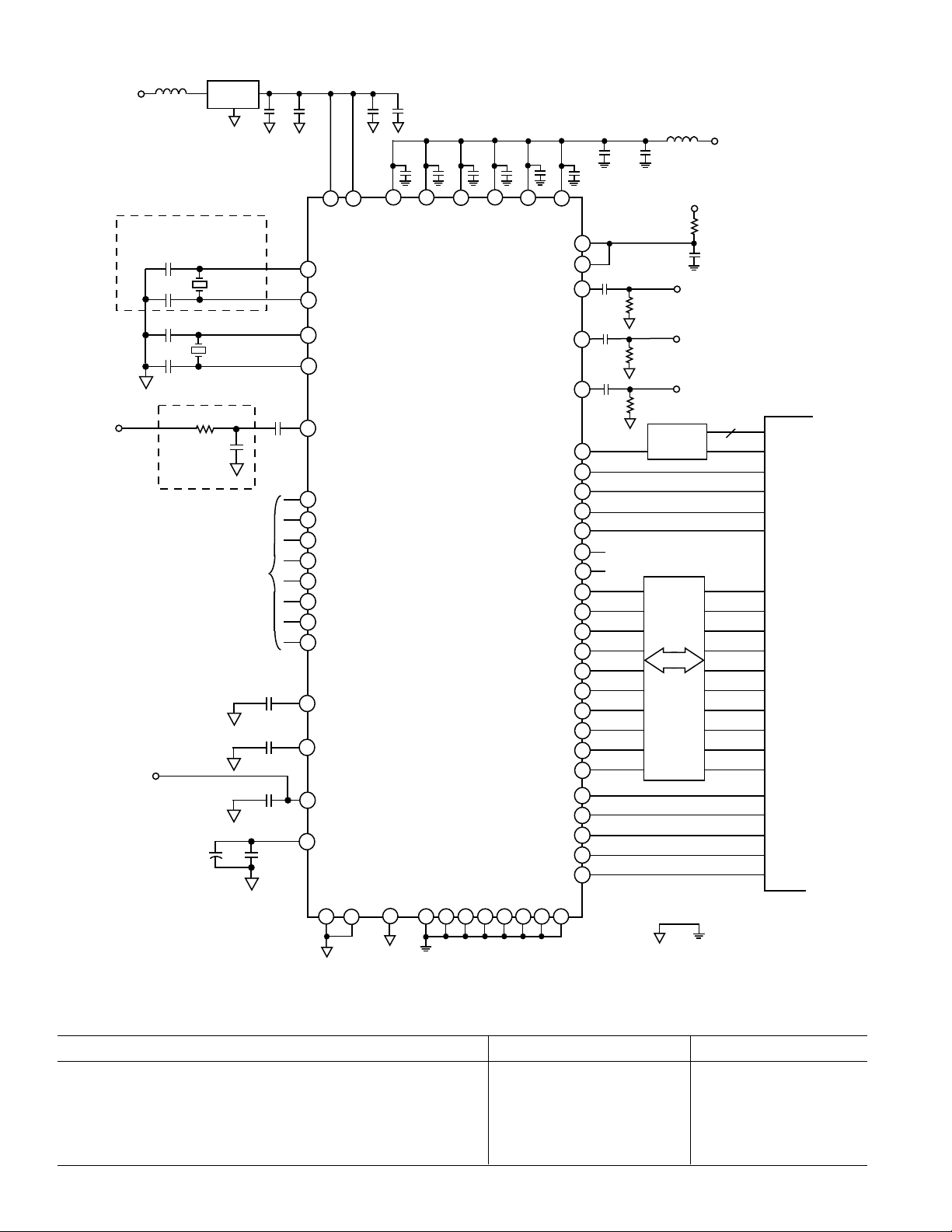
Figure 1. Highest Performance AD1845/CS4231 Codec System Diagram
Table I. Assembly Differences Between AD1845 And CS4231 For Codec “Socket” (In Figure 1)
Component Function For AD1845 Install . . . For CS4231 Install . . .
Crystal oscillator and capacitors on XTAL2 input Not required 16.9334 MHz crystal
and 33 pF (2)
Antialiasing filter on L_MIC, R_MIC, L_LINE, R_LINE, L_AUX1, 1 kΩ and 1000 pF Not required, (but can
R_AUX1, L_AUX2, R_AUX2, and M_IN inputs be left installed)
External filtering capacitors for L_FILT and R_FILT inputs 1 µF (2) 1000 pF (2)
–2–
Page 3
Input Circuit Design
AD1845
(CS4231)
2kΩ
1µF
1000pF
L_MIC (LMIC)
R_MIC (RMIC)
L_LINE (LLINE)
R_LINE (RLINE)
L_AUX1 (LAUX1)
R_AUX1 (RAUX1)
L_AUX2 (LAUX2)
R_AUX2 (RAUX2)
M_IN (MIN)
2kΩ
THE 2kΩ RESISTORS
ACT AS A VOLTAGE
DIVIDER
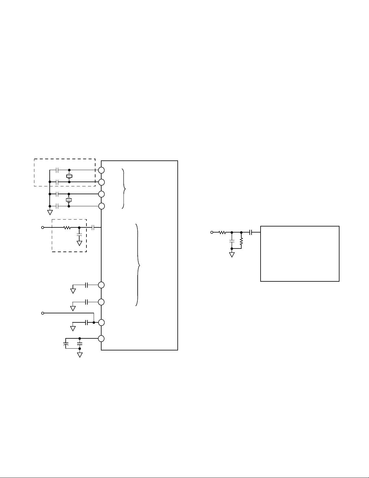
Figure 2 shows a portion of the AD1845/CS4231 system
and highlights the differences between input circuit designs for an optimum performance codec “socket.” This
section describes the following input structure differences between the codecs.
• Crystal oscillators
• Analog input filtering
Crystal Oscillator
As shown in Figure 2, the CS4231 requires two crystal
inputs, 24.575 MHz (XTAL1) and 16.9344 MHz (XTAL2).
The AD1845 defaults to one crystal input (24.576 MHz),
but also can use other frequency sources including the
14.31818 MHz PC bus clock. The AD1845 uses its Variable Sample Frequency Generator to generate any of
50,000 selectable sample rates from the single crystal
input.
CS4231
ONLY
Input Filtering
As shown in Figure 2, each of the AD1845’s ADC analog
inputs (MIC, LINE, AUX1, AUX2, & M_IN) require an external low pass antialiasing filter (1 kΩ and 1000 pF), and
the AD1845 uses 1 µF capacitors on the external filter
pins to apply a 2.6 Hz high pass filter to the ADC.
33pF
33pF
33pF
33pF
AD1845
ONLY
10µF
1kΩ
1000pF
16.9344MHz
24.576MHz
1µF
(1000pF)
1µF
(1000pF)
10µF
0.1µF
21
22
17
18
1µF
26
31
32
33
XTAL21
XTAL20
XTAL11
XTAL10
L_MIC (LMIC)
R_MIC (RMIC)
L_LINE (LLINE)
R_LINE (RLINE)
L_AUX1 (LAUX1)
R_AUX1 (RAUX1)
L_AUX2 (LAUX2)
R_AUX2 (RAUX2)
M_IN (MIN)
R_FILT (RFILT)
L_FILT (LFILT)
(VREF)
V
REF
V
(VREFI)
REF_F
Figure 2. AD1845/CS4231 Codec Input
Structures Diagram
CRYSTAL
OSCILLATOR
INPUT
DIFFERENCES
ANALOG
INPUT
FILTER
DIFFERENCES
AD1845 PLCC
(CS4231 PLCC)
The CS4231 applies its internal low pass antialiasing filtering after the input multiplexer stage and uses the external filter pins to attach 1000 pF capacitors for the low
pass filtering.
Note that for a compatible codec “socket” the external
low pass antialiasing filter required for the AD1845 is
completely compatible with the CS4231 inputs, but the
capacitors on the external filter pins MUST change for
best performance.
If you are (for example) replacing a
CS4231 with an AD1845 in your system, the two 1000 pF
capacitors must be replaced with 1 µF caps. If the
1000 pF caps are left in, the AD1845’s high pass filter
break point moves from 2.6 Hz to 2.4 kHz seriously reducing the audio band frequency performance. This performance reduction includes a nonlinear gain vs.
frequency response and an overall reduction in gain.
The gain loss can be as much as –30 dB at 20 Hz.
Optional Input Level Scaler
The two codecs have slightly different input impedances
and their data sheets provide differing designs for scaling 2 V rms line level inputs. (The AD1845 and CS4231
codecs can handle 1 V rms signals.) Figure 3 shows an
example voltage divider circuit for use with 2 V rms line
level inputs that is compatible with both codecs. For
other application related circuits, see the AD1845 and
CS4231 Data Sheets.
Figure 3. AD1845/CS4231 Codec Input Structures with
Voltage Dividers Diagram
Power Supply Design
Your power supply distribution strategy must account
for the mixed signal (analog & digital) nature of the
AD1845 and CS4231 codecs. For power supply design
considerations, think of these codecs as having a digital
section (digital portions of ADC, DAC, and ISA bus drivers) and analog section (analog portions of ADC, DAC,
multiplexer, and output mixer stages).
This section presents two successful strategies for compatible power supply design and explains what makes
the power supply strategy described by other codec
vendors’ documentation incompatible with the AD1845.
–3–
Page 4

Recommended Power Supply Design
Figure 4 shows the recommended power supply design.
This method regulates the codec’s +5 volt analog supply
from the PC’s +12 volt supply and uses the PC’s +5 volt
supply directly for the codec’s digital supply. While this
method does require more parts, the regulated analog
supply provides better noise isolation for the analog
side of the chip and yields improved converter performance. The dynamic range of this design is 1.5 dB better
than the alternate power supply method shown in Figure 5.
+5V
REGULATOR
V
V
OUT
IN
0.1µF1µF0.1µF10µF
+12V
FERRITE
BEAD
FERRITE
BEAD
0.1µF0.1µF0.1µF0.1µF0.1µF
0.1µF
10µF 0.1µF
+5V
36 35 54
V
CC
(VA2, VA1)
19
RECOMMENDED P/S FOR
AD1845 PLCC (CS4231 PLCC)
GNDA
(AGND1, 2)
34
NC
(TEST)
37
Figure 4. AD1845/CS4231 Codec Recommended Power Supply Diagram
Alternative Recommended Power Supply Design
Figure 5 shows an alternative power supply design. This
design uses the PC’s +5 volt supply for the codec’s analog and digital supplies, isolating the supplies with
small inductors (ferrite beads) to minimize stray noise
causing currents. The advantages of this supply design
are its low part count and cost reduction; each at the expense of a slightly lower dynamic range than the system
shown in Figure 4.
FERRITE
BEAD
1Ω
1µF
V
(VD4, VD3, VD1, VD2, NC, NC)
(DGND3, 4, 7, 8, 1, 2, NC, NC)
532016
+5V
0.1µF
DD
GNDD
26455
0.1µF
7115
8
FERRITE
BEAD
45
ANALOG AND DIGITALGND
44
25
CONNECTED AT ONE POINT
BENEATH CODEC
ANALOG
GND
DIGITAL
GND
1µF
0.1µF
36 35 54
V
CC
(VA2, VA1)
1519
1
(VD4, VD3, VD1, VD2, NC, NC)
7
V
DD
0.1µF0.1µF0.1µF0.1µF0.1µF
45
ALTERNATE P/S FOR
AD1845 PLCC (CS4231 PLCC)
GNDA
(AGND1, 2)
34
37
NC
(TEST)
55
(DGND3, 4, 7, 8, 1, 2, NC, NC)
GNDD
532016
2
64
44
8
25
Figure 5. AD1845/CS4231 Codec Alternate Power Supply Diagram
–4–
0.1µF
1µF
ANALOG AND DIGITAL GND
CONNECTED AT ONE POINT
BENEATH CODEC
Page 5

Avoid Vendor/Codec Specific Power Supply Design!
A third strategy for power supply design, shown in Figure 6, divides the codec into three sections (analog and
two digital). The sections are analog, internal digital,
and external digital (ISA bus drivers).
Unfortunately this
power supply design strategy yields a vendor/codec
specific system and should be avoided if you want to
design a compatible codec socket.
+5V
REGULATOR
V
V
OUT
IN
0.1µF10µF
0.1µF
1µF
+12V
FERRITE
BEAD
The problem with this particular power supply design
(recommended in some codec vendors’ documentation)
is the assumption that all codec manufacturers assign
digital power pins in the same manner. Tables II and III
show how the supply pinouts for the AD1845 and
CS4231 are (virtually) identical for a two supply design,
but differ greatly for a three supply design.
FERRITE
BEAD
0.1µF0.1µF
0.1µF0.1µF
1µF
+5V
1µF
ANALOG
RETURN
INTERNAL
DIGITAL RETURN
VENDOR/CODEC SPECIFIC TRIPLE P/S
NOT RECOMMENDED
ANALOG
SUPPLY
DIGITAL RETURN
Figure 6. Vendor/Codec Specific Power Supply Diagram—Not Recommended
Table II. AD1845 vs. CS4231 Codec Dual
Power Supply Pinout
Codec Power
Supply Line AD1845 Pinout CS4231 Pinout
Digital +5 V 1, 7, 15, 19, 45, 54 1, 7, 15, 19
45 and 54–NC)
Digital Ground 2, 8, 16, 20, 25, 44, 2, 8, 16, 20, 53,
53, 64 64 (25 and 44–NC)
Analog +5 V 35, 36 35, 36
Analog Ground 34, 37 34, 37
Table III. AD1845 vs. CS4231 Codec Triple
Power Supply Pinout
Codec Power AD1845 CS4231
Supply Line* Pinout Pinout
External Digital 1, 7, 19, 54 1, 7
(ISA Bus Driver) +5 V
External Digital 2, 8, 20, 53, 2, 8
(ISA Bus Driver) Ground 64
Internal Digital +5 V 15, 45 15, 19
Internal Digital Ground 16, 25, 44 16, 20, 53, 64
Analog +5 V 35, 36 35, 36
Analog Ground 34, 37 34, 37
*NOTE: Division of digital power among internal/external digital power
pins on Analog Devices codecs is subject to change without notice. Do
NOT base power distribution designs on the information in Table III.
EXTERNAL
DIGITAL RETURN
INTERNAL
EXTERNAL
DIGITAL RETURN
ANALOG AND DIGITALGND
CONNECTED AT ONE POINT
BENEATH CODEC
Table II shows that in the dual supply design the codecs’
power supply pinouts are identical, and Table III shows
the difference between the two codecs’ power supply
pinouts in a triple supply design.
If you use this triple
supply design, you are designing a vendor specific
system.
Suppose, for example, that you designed a triple supply
system for the AD1845. In such a system, the +5 V
regulator’s output is tied to all of the AD1845’s internal
digital power pins (15, 45), and all of the ISA driver
power pins (1, 7, 19, 54) are tied to the ISA supply. If you
needed to install the CS4231 in this system for some reason, you would find that the Crystal part will not work
because “socket” Pin 19 is connected to the ISA supply
and Pin 15 to the regulator to support the AD1845. These
two pins are connected together in the CS4231 codec
and the triple supply design for the AD1845 uses the
Crystal part as a short between the ISA supply and the
regulator’s output. If there is any substantial difference
between the ISA +5 V and the regulator +5 V, the CS4231
will (at worst) burn out or (at best) the system will not
achieve optimum performance because the digital noise
from the ISA supply is coupled through the codec onto
the analog supply.
Because triple power supply designs (recommended in
some codec vendors’ documentation) tend to treat other
vendors’ parts as a short (either through the part’s
power pins or substrate), these designs produce vendor/
codec specific systems.
Note: If you want to design a system that can use any
AD1845 compatible codec, do not use a triple power
supply design.
–5–
Page 6

Layout Design
When laying out a PCB for mixed signal devices, like
codecs, be aware that a small set of layout geometry
issues have a profound effect on component performance. This section examines the following mixed
signal PCB layout issues.
• Effects of “long-etch” impedance (impedance associated with trace between chip pin and capacitor) on
the performance of bypass capacitors, V
capaci-
REF
tors, and antialiasing circuits.
• Effects of ground and supply plane geometry on performance of mixed signal components.
This section concludes with the following guidelines for
AD1845 codec PCB design.
• A recommended ground and supply plane geometry.
• A priority list for close placement of external
components.
• A summary of recommendations for mixed signal
PCB layout.
Effects of “Long-Etch” Impedance
Bypass capacitors on your PCB are suppose to reduce
noise by acting as shorts for noise generated by digital
components and the digital side of mixed signal components. For example, a codec generates noise as it operates when its internal digital circuitry turns currents on
and off. These current changes show up on the power
and ground pins for the associated section of the codec.
For each change in power pin current, there is a change
in ground pin current. A bypass capacitor
close proximity to the part
couples stray power currents
placed in
back into the codec through the nearest ground pin.
Without bypass capacitors, these stray currents move
over nearby power/ground planes and increase the
noise of the PCB.
Close placement of bypass and filter capacitors to the
codec is crucial for a low noise PCB
. The need for close
placement of these external components stems from
the effects of long etch length between capacitors and
codec pins. At the operating frequency of the codec,
lengths of etch act as small inductors; the longer the
etch—the greater the inductance. Figure 7 shows a
representation of a bypassing circuit between a codec
power pin and ground as a capacitor in series with an
inductor. Note that the value of the inductor in Figure 7 is
directly related to the etch length between the capacitor
and the power pin.
+5V
0.1µF
CODEC POWER PIN
"LONG-ETCH" INDUCTANCE
EFFECT, APPROXIMATELY
1nH/mm
BYPASS CAPACITOR
Figure 7. “Long-Etch” Inductance Effect Model
A bypassing circuit is supposed to be a low impedance
point for high frequency currents. Because the impedance of the bypassing circuit is dependent on the distance between the capacitor and the power pin, the
“long-etch” inductance effect can force stray high frequency currents on the power pin into the part when the
part become the path of least resistance to the ground
plane. At typical codec operating frequencies for
example, a “bypass” capacitor connected to a power pin
with a 20 mm (0.5 in) trace is actually a 3.55 MHz bandpass filter.
To avoid “long-etch” effects, use the shortest possible traces for bypass and filter capacitors. Also note
that using 3 to 5 mm wide etches for capacitor connections reduces inductance effects as well (highly
recommended).
The AD1845 is available in PLCC or TQFP packages. The
small physical dimensions of these packages can make it
challenging to place all the required capacitors close to
the part. Because some pins have a much greater effect
on performance than others, use the information in
Table IV to prioritize component placement. Pins with an
“A” priority in Table IV should be connected to their associated capacitors with the shortest traces possible.
Figure 8 also shows the distribution of codec bypass and
filter capacitor locations and placement priorities.
Table IV. AD1845 Compatible Codec Capacitor Placement Priorities
Priority of Close Proximity to Chip Pin
Signal Description PLCC Package Pins Placement of Filter and Decoupling Capacitors
Voltage Reference (V
Voltage Reference Filter (V
)32 A
REF
_F) 33 A
REF
Digital Supply Voltage, +5 V (VDD) 1, 7, 15, 19, 45, 54 B
Channel Filters (L_FILT and R_FILT) 26, 31 B
Analog Supply Voltage, +5 V (VCC) 35, 36 C
Analog Signal Inputs (Filter and Decouple) 27, 28, 29, 30, 38, D
(L_LINE, R_LINE, L_MIC, R_MIC, L_AUX1, 39, 42, 43, 46
R_AUX1, L_AUX2, R_AUX2, & M_IN)
–6–
Page 7

Effects of Ground and Supply Plane Geometry
Figure 8 shows an example ground plane layout for an
AD1845 PLCC package. This layout separates the analog
and digital ground planes with a 2 to 3 mm gap and connects them at one point beneath the codec with a single
3 to 4 mm wide link. The ground planes reduce board
noise by “shielding” analog lines from digital interference. The link between the planes, as close to the codec
as possible, prevents any potential difference due to
ESD or fault currents. Without the link, these currents
could flow through the codec’s substrate degrading performance. You should try to avoid running any digital or
analog signal traces across the gap between the digital
and analog planes.
DIGITAL GROUND
CODEC PIN NUMBERS
B
9
10
B
AD1845
PLANE
61
60
B
COMPATIBLE
B
B
26
PRIORITY LEVEL FOR CLOSE
PROXIMITY PLACEMENT
OF FILTER & DECOUPLING
CAPACITORS (A, B, & C)
PLCC FOOTPRINT
27
B CD D D D DDDD D
ABCA
43
B
44
ANALOG
GROUND
PLANE
Figure 8. AD1845 Compatible Codec Recommended
Ground Plane and Capacitor Placement
During PCB development, you may find it useful to provide removable links between the ground planes in several PCB locations, to permit debugging and testing for
ground isolation.
Another way to reduce PCB noise, in addition to ground
planes, is to include separate digital and analog
supply
planes directly over their respective
power
ground
planes—no overlapping of supply planes. The supply
and ground plane pairs should be separated by approximately 1 mm. This recommendation implies that you
use a four layer PCB (at least) with the ground and
power planes forming a high capacitive “sandwich.”
This layout technique yields an extremely effective, low
ESR/low ESL power distribution scheme.
For a layout that helps reduce noise, locate all digital
components over the digital power/ground plane sandwich and all analog components over the analog power/
ground plane sandwich. Though this technique does not
eliminate the need for bypass capacitors at the power
pins (mentioned above), the importance of power/
ground planes in reducing overall PCB noise cannot be
over emphasized.
Digital noise coupled onto the analog portion of the chip
has three possible current return routes. The first return
path is back through V
and VDD where the currents are
CC
capacitively coupled to their respective ground planes.
The second possible path is through the component’s
substrate which has an ≈10 Ω characteristic impedance.
The final return path is through the external analog and
digital ground plane connection.
By keeping the ground plane connection as close to the
part as possible, the ground connection becomes the
path of least resistance and minimizes the amount of
digital current pushed into the substrate. If the ground
connection is a long distance from the part, returning
current tends to use the substrate connection—
increasing signal noise in the part.
This current path example is simplistic and is only a
model of how a PCB’s layout can help reduce noise. For
more information on how noise coupling really works,
see any of the texts listed in the References section.
Codec PCB Layout Strategy Summary
This section summarizes the layout suggestions for an
AD1845 compatible codec “socket.” To get the best
performance from the codec in your system, apply the
following principles to your board’s layout:
• Locate filter and decoupling capacitors as close as
possible to their corresponding codec pins (Table IV
and Figure 8 describe the specifics and priorities this
process entails for an AD1845/CS4231 “socket”).
Close placement of capacitors to the chip pins helps
to avoid noise related to long-trace inductance
effects.
• Use a split (separate analog and digital) ground plane
and matching non-overlapping +5 V supply planes.
The power and ground planes should be separated
by approximately 1 mm (i.e., four layer PCB). A single
3 to 4 mm wide link under the codec connects the
ground planes (see Figure 8). Matching ground and
power planes provide a highly effective low ESR and
low ESL bypass capacitor for the system.
• Locate analog and digital components only over their
respective ground planes and decouple their power
pins as closely to the chip pin as possible. Route analog and digital signal traces only over their respective
ground planes. These steps greatly reduce noise in
the analog section.
• Avoid using IC sockets for any analog components.
• Enable only a single oscillator on a PC board at a time
(if possible). This is not always a problem, but be
aware that some system problems can occur as a
result of interference frequencies between multiple
crystal oscillators entering the codec through the
analog or digital supplies or signal/reference pins.
–7–
Page 8

Table V. Codec System Design Cost/Performance Tradeoffs
Cost Reduction Design Choice Resulting Performance Tradeoff
Use .3 µF capacitors on the external filter pins While this method eliminates an assembly difference between
for both the AD1845 and CS4231. using the codecs, the drawback of using .3 µF capacitors is degraded
performance of both parts. A CS4231 in such a design has reduced
high frequency performance and an AD1845 has reduced low frequency performance.
Eliminate external antialiasing filter circuits. While it is possible to use the AD1845 without antialiasing filters (the
CS4231 does not need them), the drawback of this design choice is
that codec performance can be dramatically affected if noise is
capacitively coupled into the ADC’s inputs.
Reduce the number of bypass capacitors While this method does reduces part count and cost, the placement of
through having common sectional power pins of the remaining capacitors becomes more difficult, bypassing
use the same capacitor for bypassing. efficiency is reduced, and the sound card has more noise problems.
• Minimize capacitive loading on digital output pins.
For digital signals, driving “long” traces, you may
have to terminate the trace in its characteristic impedance (typically 100 Ω) to prevent over/undershoot and
ringing.
CONCLUSION
Placing an AD1845/CS4231 compatible codec “socket”
on your PC motherboard or plug-in card design is not
difficult. For optimum performance from each part, such
a “socket”—using a PCB layout common to both parts—
does entail minor assembly differences between the
• Be aware of the effects that inductor/transformer’s
external magnetic fields may have on analog circuitry. Use electrostatic and magnetically shielded
components as necessary. RF decoupling chokes
mounted at right angles minimize mutual inductance.
Mount power transformers off the board and orient
them with the most intense area of their external
codecs (see Table I and Figure 1). Using the guidelines
in the
Cost Vs. Performance Design
section, you can
design a compatible codec “socket” that does not require any external component differences besides the
codec (with some loss in performance). For more information on application circuits for the AD1845, see the
AD1845 data sheet and the reference documents listed.
fields away from critical analog circuits. Use toroidal
power transformers to minimize external fields.
• Shield analog I/O lines by running “shield” traces between them and/or running them over an analog
ground plane.
COST VS. PERFORMANCE DESIGN
Sometimes lower cost is much more important than
high performance. Table V lists methods for cutting systems costs and describes their corresponding perfor-
REFERENCES
The sources listed below contributed information to this
applications note. They provide recommendations and
techniques for high-speed and mixed-signal design:
Mixed Signal Processing Design Seminar
, Analog De-
vices, Inc., 1991, ISBN-0-916550-08-7.
High Speed Design Seminar
, Analog Devices, Inc., 1990,
ISBN 0-916550-07-9.
mance reduction.
Applications Reference Manual
, Analog Devices, Inc.,
1993. Especially refer to collected Application Notes—
Section 24—AN-214, AN-280, AN-282, AN-345, AN-346,
AN-347, AN-353, AN-362.
E2039–5–8/95
Noise Reduction Techniques in Electronic Systems
Ed, Henry W. Ott, Wiley Interscience, 1988.
Interfacing Techniques in Digital Design With Emphasis
on Microprocessors
Audio/Video Reference Manual
, Ronald L. Krutz, John Wiley, 1988.
, Analog Devices, Inc.,
1992.
Systems Application Guide
, Analog Devices, Inc., 1993,
ISBN 0-916550-13-3.
High-Speed Digital Design, A Handbook of Black Magic
H. W. Johnson, M. Graham, PTR Prentice Hall, 1993.
ISBN 0-13-395724-1.
–8–
, 2nd
PRINTED IN U.S.A.
,
 Loading...