

Page 1
AN-402
a
ONE TECHNOLOGY WAY • P.O. BOX 9106
Replacing Output Clamping Op Amps with Input Clamping Amps
INTRODUCTION
Various systems like ultrasound and imaging systems,
have instances where the analog signal might suddenly
spike to a voltage extreme. But many downstream circuits like A/D drivers place restrictions on the analog input signal levels in order to maintain their performance.
These devices can draw excessive current in an overdrive condition or else be driven into a region of saturation which will have a long recovery time.
Various clamp amps can be used in these systems to restrict signal excursions at their outputs to protect downstream devices. So far most of the clamping amplifiers
have relied upon an output clamping architecture and
are called output clamp amps (OCAs). A new architecture called an input clamp amp (ICA) offers superior
clamping accuracy and lower distortion.
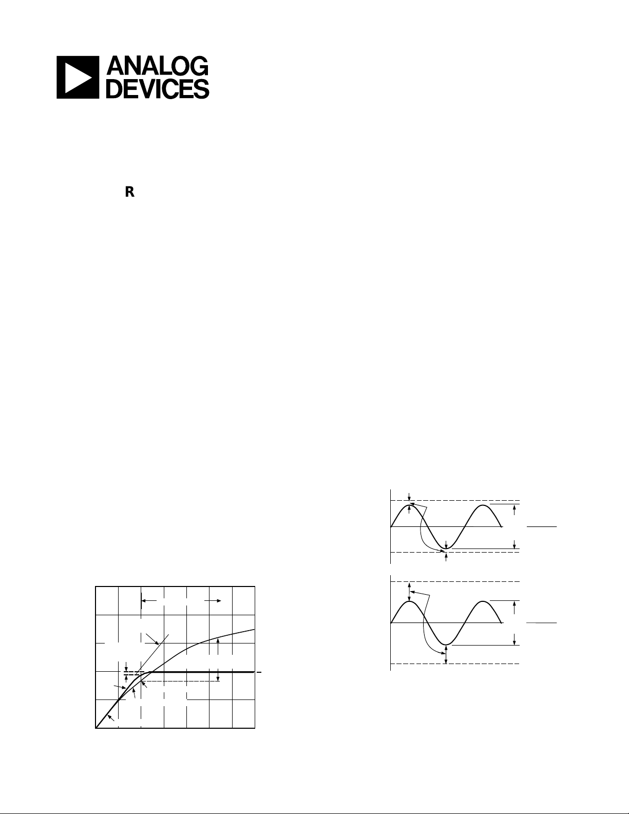
Figure 1 illustrates the relative performance of the two
devices. It can be seen that the ICA more closely tracks a
straight line in the linear region up to the point that it
bends over into the clamp region. On the other hand, the
OCA breaks away from a straight line sooner as it approaches the clamp voltage. Of course the extent to
which the response more closely tracks a straight line is
indicative of the amplifier’s linearity in that region.
1.6
CLAMP REGION
1.4
OUT
1.2
1.0
AD8036
OUTPUT VOLTAGE – V
0.8
0.6
0.6 2.00.8 1.0 1.2 1.4 1.6 1.8
Figure 1. Output Clamp Error vs. Input Clamp Error
LINEAR
EXTENSION
CLAMP
ERROR – 25mV
AD8036
(ICA)
OUTPUT CLAMP AMP
LINEAR REGION
CLAMP ERROR – >200mV
OUTPUT CLAMP
NEAR CLAMP REGION
INPUT VOLTAGE – +V
IN
CLAMP
LEVEL
•
NORWOOD, MASSACHUSETTS 02062-9106
APPLICATION NOTE
617/329-4700
•
To compensate for this added distortion, OCAs are required to have their clamping levels set wider than the
maximum excursion of interest if minimum distortion is
desired. Therefore, when substituting an ICA for an
OCA, the clamp region can be narrowed without adding
extra distortion. This will lower the voltages experienced by downstream circuitry during overdrive. In
most designs, making this adjustment requires only a
minor modification to the circuit that generates the
clamp voltages.
Figure 2 illustrates this concept. The amplitude of the
linear signal for each type of amplifier is the same. However, the upper and lower clamp levels of the OCA must
be set wider in order to preserve the signal linearity due
to the larger near-clamp distortion region. Thus for overdrive conditions, the downstream circuitry will see
larger signals when driven by an OCA than an ICA.
NEAR CLAMP
DISTORTION
INPUT
CLAMP
AMP
OUTPUT
CLAMP
AMP
REGION
NEAR CLAMP
DISTORTION
REGION
Figure 2. Comparison of Near-Clamp Distortion
Regions of ICA vs. OCA
In addition the overdrive response will be further improved as a result of the superior overdrive characteristics of the ICA. The output of an ICA will not go more
than 10 mV past the level set by the clamps for clamping
stages with low gain. On the other hand, an OCA will
HIGH CLAMP LEVEL
MAX
LINEAR
SIGNAL
REGION
LOW CLAMP LEVEL
HIGH CLAMP LEVEL
MAX
LINEAR
SIGNAL
LOW CLAMP LEVEL
Page 2
overshoot by a few hundred millivolts depending on the
magnitude of the overdrive signal. Once again Figure 1
illustrates this concept. The ICA performance can be
seen to be relatively flat in the clamp region independent of the magnitude of the overdrive, while the OCA
output keeps on increasing along with increasing overdrive amplitude.
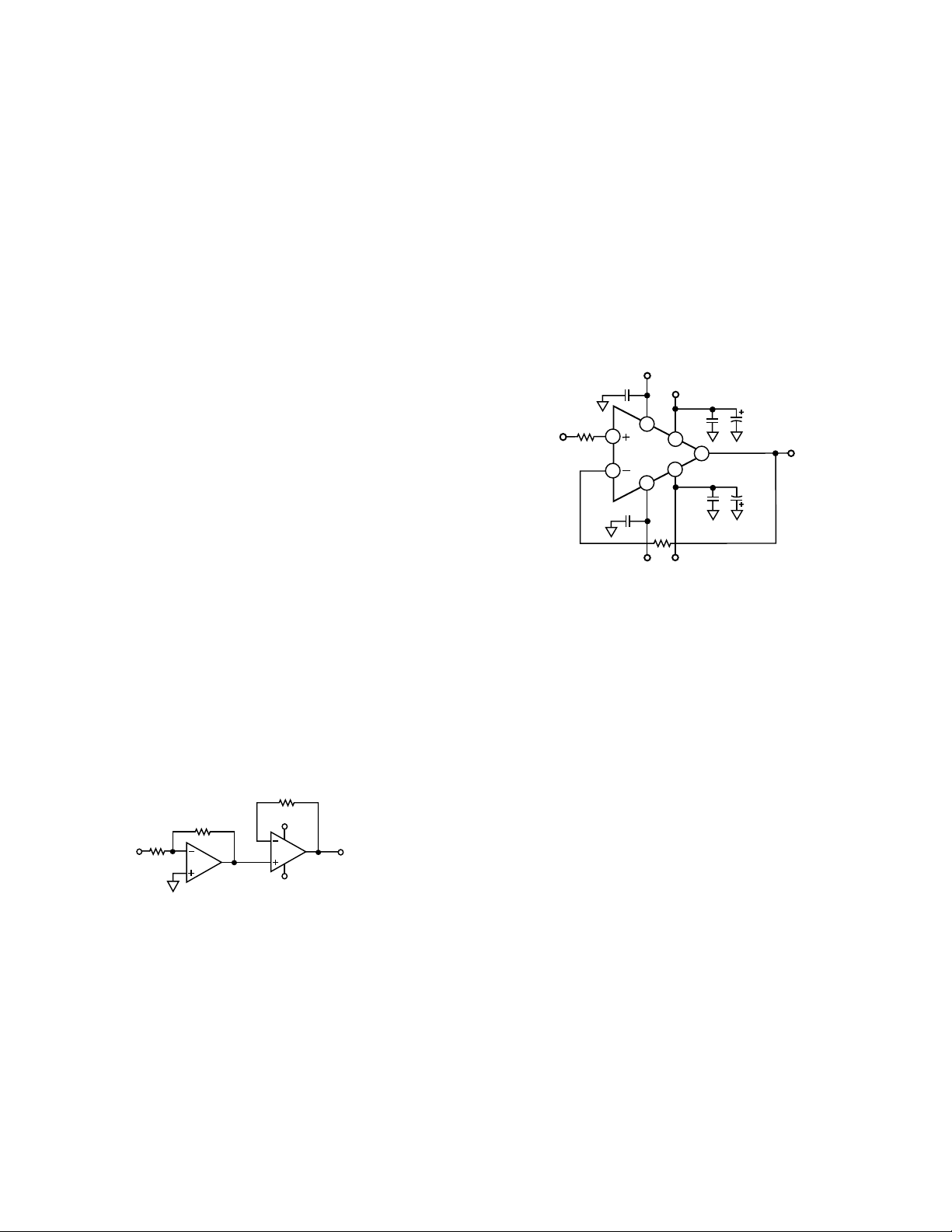
NONINVERTING OPERATION
Unity Gain
For the case of substituting for a noninverting OCA, the
most important consideration is the gain at which the
clamp amp is operating. This is because the output
clamping level for an ICA is a function of the closed loop
gain of the amplifier.
The first two input clamp amps, the AD8036 and
AD8037, introduced by Analog Devices operate with an
ICA structure. But because of differences in their operation, except for circuits that operate with a gain of +1,
substituting an ICA into a design that has been implemented with an OCA is not a “drop-in” replacement,
even though the pinouts of the parts are identical. However, because the pinouts are identical, the required circuit modifications will, in general, be not too extensive.
Each configuration though must be handled on a caseby-case basis. The following details the considerations
for making this substitution.
Inverting Operation
The first consideration is the polarity of operation of the
op amp. The input clamping op amp architecture of the
AD8036 and AD8037 does not operate in the inverting
mode. Therefore it is not possible to directly replace an
OCA with an ICA for inverting configurations. In order to
benefit from the ICA’s superior clamping characteristics
in inverting applications, a separate inverting stage is
required.
Figure 3 shows a circuit with an inverting stage followed
by an ICA, the AD8036 in a noninverting configuration
for providing the overall function of an inverting clamping amplifier. The circuit shown will have a gain of
–R
and will clamp at VH and VL. The operation of the
F/RI
clamping stage will be explained further in the next section. In all clamp circuits, V
must be greater than VL, but
H
the two can be anywhere within the output range of the
part.
140Ω
V
R
F
R
I
V
IN
2
6
3
H
2
8
V
6
H
3
V
L
AD8036
5
V
L
V
OUT
Figure 3. Inverting Clamping Circuit
For circuits that require a gain of more than (minus) 1,
the designer has a choice as to how to distribute the
gain between the inverting stage and the clamp stage.
For greatest accuracy, the ICA should operate at lower
gains because the clamp accuracy is a function of the
gain as will be detailed in the next section. Additional
required gain can be provided in the inverting stage.
The first case to consider is a noninverting unity gain.
For OCAs, the clamping levels are simply equal to the
voltages applied to V
(Pin 8) and VL (Pin 5). For an ICA,
H
these voltages are multiplied by the closed loop gain in
order to calculate the clamping levels. But since the gain
is +1, the ICA and OCA will both have the same clamping
levels. Thus, a direct substitution can be made. Figure 4
is an example of a unity gain clamping circuit.
V
CH
0.1µF
100Ω
V
IN
3
2
0.1µF
8
V
H
AD8036
V
L
5
300Ω
V
CL
+5V
0.1µF
7
4
0.1µF
R
F
–5V
10µF
6
10µF
V
OUT
Figure 4. Unity Gain Noninverting Clamp
Since we are talking about a noninverting unity gain, the
amplifier chosen must also exhibit stable operation at
unity gain. Of the two ICAs, the AD8036 is compensated
for operation at unity gain. Thus, the AD8036 is a “drop
in” replacement for an OCA in noninverting unity gain
applications. It will provide the same gain and clamp at
the same levels as the OCA.
Gains of Two or More
When the noninverting gain of the clamp amp is two or
greater, the AD8037 can be used for its wider bandwidth, as it is compensated for noise gains of two or
greater. However, the voltages applied to the clamp pins
will have to be changed to maintain the same clamping
levels, because the clamping levels are a function of the
closed loop gain of the amplifier. The following equations summarize the calculations for obtaining the
proper clamp voltages:
V
= G ×
= G ×
V
H
V
L
where: V
CH
V
CL
is the high output clamping level
CH
V
is the low output clamping level
CL
G is the gain of the amplifier configuration
V
is the voltage applied to VH (Pin 8)
H
V
is the voltage applied to VL (Pin 5)
L
–2–
Page 3

In general, to maintain the same clamping levels as for
an OCA, the voltage applied to either clamp pin should
be set at the value desired for the clamp level divided by
the closed-loop gain of the amplifier. For example, if the
amplifier operates at a gain of two and it is desired to
clamp on the high side at 1 V, then the voltage applied to
V
(Pin 8) should be 1 V/2 or 0.5 V. Similarly, if it is de-
H
sired to set the lower clamp at –1 V, then the voltage
applied to V
(Pin 5) should be –1 V/2 or –0.5 V. Fig-
L
ure 5 is a schematic for a clamping stage using an
AD8037 with a gain of 2.
V
H
0.1µF
V
100Ω
IN
R
G
274Ω
3
49.9Ω
2
0.1µF
8
V
H
AD8036
V
L
5
274Ω
V
L
+5V
0.1µF
7
4
0.1µF
R
F
–5V
10µF
6
10µF
V
OUT
Figure 5. Gain-of-Two Noninverting Clamp
The above implies that an input offset in the clamp circuit will be multiplied by the gain of the op amp stage.
To obtain the best clamping accuracy, the clamp amp
should be set for a low gain and any additional necessary gain be provided by another gain stage prior to the
clamping stage. The greater accuracy of an ICA over an
OCA can be practically realized for clamping stages with
gain of up to 10.
The discussion of distortion in the near-clamp region
still applies. The clamping window must be slightly
larger than the maximum signal excursion for which
lowest distortion is desired. A/Ds will have a region between maximum signal level to be converted and maxi-
mum overdrive signal level that does not compromise
its specifications. It is within this region that the clamping levels should be set.
Clamping with an Offset
Some op amp applications require a dc offset voltage at
their output. These are generally configured in the inverting mode where the offset can be produced by a dc
voltage that is simply summed through a summing resistor as an additional input to the amplifier. Since an
ICA does not support inverting mode clamping, it is not
possible to clamp with this configuration.
Noninverting circuits can be created that offer both gain
and offset. However, because there is an interaction
among the resistors used to vary the gain and offset,
the design is not as straightforward as for inverting
configurations.
Figure 6 shows a noninverting configuration of an
AD8037 that provides clamping and also has an
offset. The circuit shows a driver for an AD9002, an 8-bit,
125 MSPS A/D converter and illustrates some of the considerations for using an AD8037 with offset and clamping. The analog input range of the AD9002 is from
ground to –2 V. The input should not go far outside of
this range in order to avoid drawing excessive current.
The input is symmetrical about ground with an amplitude of 1 V p-p.
For the AD8037 to operate at a gain of two, a 301 Ω feedback resistor is chosen as recommended by the data
sheet. For a gain of two the parallel combination of resistors R1 and R3 must be equal to the feedback resistor
R2. Thus
R
1 × R3/(R1 + R3) = R2 = 301 Ω
The reference used to provide the offset is the AD780
whose output is 2.5 V. To find the value of R3, first assume that the input at the noninverting input is at 0 V.
This will force the inverting input to also be at 0 V, which
+5V
806Ω
8
V
H
AD8037
V
L
5
–5V
R2
301Ω
0.1µF
+5V
–5V
7
4
0.1µF
0.1µF
6
–2V to 0V
10µF
10µF
1N5712
49.9Ω
CLAMPING
RANGE
–2.1V to +0.1V
0.1µF
AD9002
V
= –2V TO 0V
IN
SUBSTRATE
DIODE
–5.2V
10µF
0.1µF
+5V
AD780
V
IN
–0.5V to +0.5V
2.5V
0.1µF
49.9Ω
R3
750Ω
499Ω
0.1µF
R1
100Ω
100Ω
3
2
100Ω
806Ω
Figure 6. Gain of Two, Noninverting with Offset AD8037 Driving an AD9002—8-Bit, 125 MSPS A/D Converter
–3–
Page 4

creates a condition where no current flows through R2.
The output now wants to be at –1 V (midpoint of range
that corresponds to input midpoint), so a current of
1 V/301 Ω or 3.32 mA will flow in R2. Since no current
flows in either R1 or into the inverting input of the op
amp, this same current must flow in R3. Thus
2.5
V
= (3.32 mA) R3 or R3 = 750 Ω.
The above equation then yields a value for R1 of 499 Ω.
It is desirable to clamp the signal so that the output goes
no more than 100 mV outside of the A/D’s maximum input signal range in either direction. Thus the high level
clamping should occur at +0.1 V and the low level
clamping should occur at –2.1 V as seen at the output.
Because the clamping is done at the input stage, a
clamping level as seen at the output is affected by not
only the gain of the circuit as previously described, but
also by the offset. Thus, in order to obtain the clamping
levels desired, V
must be biased at +550 mV, while V
H
must be biased at –550 mV. The voltage dividers created
by the 806 Ω and 100 Ω resistors between the supplies
and ground are used to create the clamp voltages.
In general the clamping levels as seen at the output can
be calculated by the following:
V
=
V
+ G ×
+ G ×
V
V
H
L
where V
CH
OFF
V
=
V
CL
OFF
is the offset voltage that appears at the
OFF
output.
Another way to look at setting the clamp levels is by not-
ing that the clamp signals (V
and VL) are alternate non-
H
inverting inputs that are selected when the conventional
noninverting input goes outside the “window” that they
establish. See Figure 7. It is desired to clamp 100 mV
higher and lower than the maximum excursion of the
input signal with a gain of two. Therefore, V
should be
H
50 mV above the maximum input signal excursion of
+0.5 V or +550 mV. Likewise, V
should be 50 mV below
L
the minimum input signal excursion of –0.5 V or
–550 mV. The 50 mV in each case will be multiplied by
two to yield 100 mV, while the same offset will be applied to both the input signal and the clamps.
R
F
140Ω
–V
IN
+V
IN
V
V
+1
+1
H
+1
L
A
S1
B
C
C
H
C
L
A1
S1
> V
V
IN
H
VL ≤ VIN ≤ V
< V
V
IN
L
H
A2
+1
A B C
0 1 0
1 0 0
0 0 1
V
OUT
E2089–9–11/95
Figure 7. AD8036/AD8037 Clamp Amp System
The 1N5712 Schottky diode is used for protection from
L
forward biasing the substrate diode in the AD9002 during power up transients.
OTHER CONSIDERATIONS
In general, the resistors used to generate the voltages
for V
and VL should be kept below 1k. This will minimize
H
errors due to bias current. It is also recommended to use
a 0.1 µF capacitor to ground close to the op amp for bypassing V
and VL. If one or both of the clamp inputs is
H
not used, the pin or pins can be left floating and the amplifier will function the same as one without clamping. If
the either or both clamp pins are dynamically driven and
it is desired to create a nonclamping situation, then V
H
can be biased at +V for no clamping for positive excursions, while V
can be biased at –V for no clamping at
L
negative excursions.
CONCLUSION
Input clamp amps (ICAs) offer superior clamping performance than output clamp amps (OCAs). For most applications an ICA can be used to replace an OCA, but
depending on various circuit details, modifications will
have to be made to successfully complete the change.
The successful use of ICAs requires that each circuit be
approached on a case-by-case basis. The techniques
offered describe the circuit changes required to handle
the most common situations.
–4–
PRINTED IN U.S.A.
 Loading...