

Page 1
AN-399
a
ONE TECHNOLOGY WAY • P.O. BOX 9106
Interfacing the AD1890/AD1891 to AES/EBU Receivers and Digital Filters
by Hank Zumbahlen, Senior Field Applications Engineer
ABSTRACT
The AES/EBU AES3-199X and the IEC-958 have become
the standard for interfacing digital audio components in
the digital domain. The AD1890/AD1891 Asynchronous
Sample Rate Converter (ASRC) is a device that provides a solution to sample rate interfacing and
compatibility issues. The practice of using oversampling
the digital signal before it goes to the digital-to-analog
converter has become standard as well. This paper
examines the issues with interfacing these components.
THE AES/EBU INPUT
Even though the resolution of commercial digital audio
sources, the Compact Disc (CD) and Digital Audio Tape
(DAT), is 16 bits, the AES/EBU interface has space for 20
bits of data, out of a total frame size of 32 bits. The
format for the subframe is shown in Figure 1. This
allows higher resolution in professional applications.
Therefore, since the data will not fill up the entire width
of the word, the data must be padded. This padding can
either be before or after the data word. If it is placed
before the data, the LSB (Least Significant Bit) is in the
32nd clock position. This is referred to as right-justified
data. If the padding is placed after the data, the MSB
(Most Significant Bit) is in the first clock position. This is
referred to as left-justified data.
•
APPLICATION NOTE
NORWOOD, MASSACHUSETTS 02062-9106
The problem arises when you try to mate a component
that right justifies the data with one that expects leftjustified data. This is the case when trying to mate the
AD1890/AD1891 with the Yamaha YM3623B receiver
chip. The Crystal CS8412 allows the user to select which
data format is to be used. These two chips are by far the
most popular solutions at this point in time.
The standard digital audio signal set consists of the data,
which is alternated between the left and right channels,
a signal to indicate whether it is the left or right channel
(L/R), a bit clock and a word clock which indicates valid
data. It is by moving the L/R clock that we can change the
justification of the data.
Assume that we have 16 bits of right-justified data,
which is the case with the Yamaha part. That would
mean that we would have 16 leading zeros. By delaying
the L/R clock, outputted by the receiver chip, by the word
clock, also an output from the receiver chip, we delay the
L/R clock by a quarter cycle. The L/R signal will now
change state at the beginning of valid output data, which
in effect changes the data to left justification. This
delaying of the L/R clock is done simply with a D type
flip-flop (see Figure 2). The timing signals are given in
Figure 3.
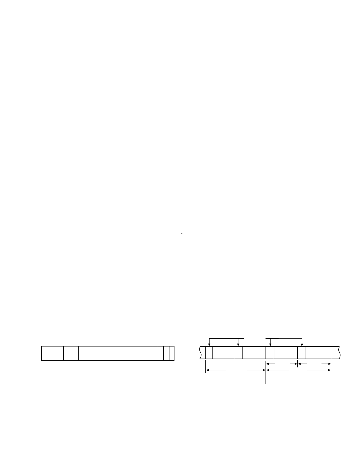
PREAMBLE
•
617/329-4700
L
AUX
PREAMBLE
BIT 0 3 4 7 8
PREAMBLE – INDENTIFIES RIGHT OR LEFT CHANNEL AND START OF BLOCK
AUX DATA – AUDIO DATA IF DATA WORD GREATER THAN 20 BITS
V – VALIDITY BIT 0 = VALID DATA
U – USER DATA BIT UNDEFINED
C – CHANNEL STATUS BIT
P – PARITY BIT GENERATES EVEN PARITY
S
DATA
B
– OPEN FOR OTHER APPLICATIONS IF DATA WORD IS
LESS THAN 20 BITS
AUDIO DATA
M
S
VUCP
B
27 28 29 30 31
Figure 1a. Audio Subframe Format
CH A
A
DATA
FRAME 191
PREAMBLE A – INDICATES CH A DATA
B – INDICATES CH B DATA
S – INDICATES CH A DATA AND START OF
CH B
B
DATA
END OF
STATUS BLOCK
STATUS BLOCK
CH A
S
DATA
SUB
FRAME
START OF
STATUS BLOCK
Figure 1b. Audio Block Format
B
FRAME 0
CH B
DATA
SUB
FRAME
Page 2
YM3623B
28
DIN
6
XIN
5
XOUT
2
ADJ
3
VCO
7
KMODE/
22
SEL
SCLK
SSYNC
25 26 13 18
ADDITIONAL CIRCUITRY NOT SHOWN FOR CLARITY
SDO
27
DOUT
CLK
L/R
EMP
HLDR
HLDL
ØA
ØB
ERR
SYNC/
17
12
15
16
19
20
8
9
23
S1
24
S2
21
WC
+V
4
2
PR
DQ
3
CLK
CL
1
74HC74
+V
5
6
Q
+V
D
3
DATA_I
4
BCLK_I
6
L/R_I
5
WCLK_I
10
BKPOL_I
11
TRGLR_I
12
MSBDLY_I
GPDLYS
12827 13 2
AD1891
DATA_O
BCLK_O
WCLK_O
BKPOL_O
TRGLR_O
MSBDLY_O
MUTE_O
FLAG_I
RESET
L/R_O
MUTE_I
SEETLSLW
MCLK
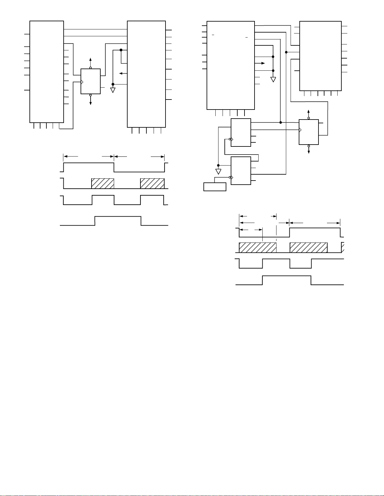
Figure 2. Justification Change
YM3623B
PIN
15
17
WORD
18
CLOCK
AD1890/91
PIN
5
32 CLOCKS
L/R
DATA
L/R
32 CLOCKS
Figure 3. AES Receiver - ASRC Timing
THE INTERPOLATION FILTER
Just the inverse process is required for interfacing to the
NPC SM5813 and similar digital filters. These filters are
used to raise the apparent sample rate of the digital
audio string by a factor of, typically, 4 or 8. By increasing
the apparent data rate the images are moved out in
frequency so that a much simpler (lower order) filter can
be designed. The advantages of a simpler filter are
many. First and most important is that a smaller filter is
easier to design and manufacture. They use less
components so they are less expensive. Also, a low
order filter will not have high “Q” sections which tend to
ring when hit with a transient.
The filter is expecting right hand justified data. The
AD1890/AD1891 outputs left-hand justified data.
Therefore we must use the same trick we used before
(see Figure 4). The L/R clock is delayed by the word clock
to effectively change the justification of the data from
left-justified to right-justified.
There is a slight difference though. The AD1890/AD1891
will put out 24 bits of data. The digital filter is expecting
only 16 bits. Luckily the data format is MSB first so that
the first 16 bits will be latched in when the L/R clock
transitions, which latches the contents of the digital
filters shift register. The remaining bits will not affect the
input to the filter, since the shift register is only sixteen
bits wide and the last bits of the previous channel will
have shifted all the way through the register before the
valid bits for the present channel are latched. Figure 5
shows the timing for the ASRC-filter interface.
3
23
26
24
25
19
18
17
DATA_I
4
BCLK_I
6
L/R_I
5
WCLK_I
10
BKPOL_I
11
TRGLR_I
12
MSBDLY_I
WCLK_O
BKPOL_O
TRGLR_O
MSBDLY_O
AD1890
16
15
GPDLYS
FLAG_I
RESET
12827 13 2
2
CLR
1
A
74HC393
12
CLR
13
3
CLKOUT
A
74HC393
12.288 MHz
23
DATA_O
26
BCLK_O
24
L/R_O
25
19
18
+V
17
16
MUTE_O
15
MUTE_I
SEETLSLW
MCLK
L/R
6
QD
WORD CLOCK
5
QC
4
QB
3
QA
8
QD
9
QC
10
BIT CLOCK
QB
11
QA
ADDITIONAL CIRCUITRY NOT SHOWN FOR CLARITY
6
XT1
7
XT0
NPC5813
1
DIN
2
BCLK
28
L/R
14
/RST
/CKDV
/CKSL
/SYN
43
10 15 17 16
+V
4
2
D
3
CLK
1
PR
CL
+V
5
Q
6
Q
74HC74
FSCO
WCKO
BCKO
/COB
CKO
DOL
DOR
DG
/OW18
9
27
24
23
25
26
20
/OW20
E2037–15–6/95
Figure 4. Digital Filter Interface
24 CLOCKS
AD1890/91
PIN
24
DATA
23
WORD
CLOCK
NPC5813
PIN
28
L/R
L/R
16
CLOCKS
32 CLOCKS
32 CLOCKS
Figure 5. ASRC-Digital Filter Timing
CONCLUSION
The interface between components which expect
different justification of data has been examined. A
proposal for modifying the justification has been
presented. It should be noted that second generation
ASRCs, the AD1893, have internal provisions for
selection either left justification or right justification.
BIBLIOGRAPHY
1) AUDIO ENGINEERING SOCIETY, “AES Recommended Practice for Digital Audio Engineering – Serial
Transmission Format for Linearly Represented
Digital Audio Data,” AES3-1985 (ANSI S4.40-1985).
2) INTERNATIONAL ELECTROTECHNICAL COMMISSION ,
PRINTED IN U.S.A.
“International Standard Digital Audio Interface,” IEC
958 1989.
3) Zumbahlen, Hank, “An Outboard Digital-to-Analog
Converter for Digital Audio Sources,” Analog Devices
AN-394, 1995.
4) Sanchez, Clifton & Taylor, Robert, “Overview of Digital Audio Interface Structures,” Crystal Semiconductor AN-22.
–2–
 Loading...