

AN-398
a
ONE TECHNOLOGY WAY • P.O. BOX 9106
Evaluation Boards for Single, Dual, and Quad Operational Amplifiers
INTRODUCTION
This application note describes evaluation boards for
single, dual, and quad operational amplifiers whose pinouts follow industry standard amplifier sockets. These
blank printed circuit boards are available to qualified
OEMs at no charge, and were designed to provide quick
and easy evaluation of precision and medium-speed
(gain-bandwidth products < 10 MHz) operational amplifiers in inverting and noninverting applications. Furthermore, provisions have been made on the boards to
evaluate operational amplifier capacitive loading effects
using inside-the-loop or outside-the-loop capacitive
load compensation techniques.
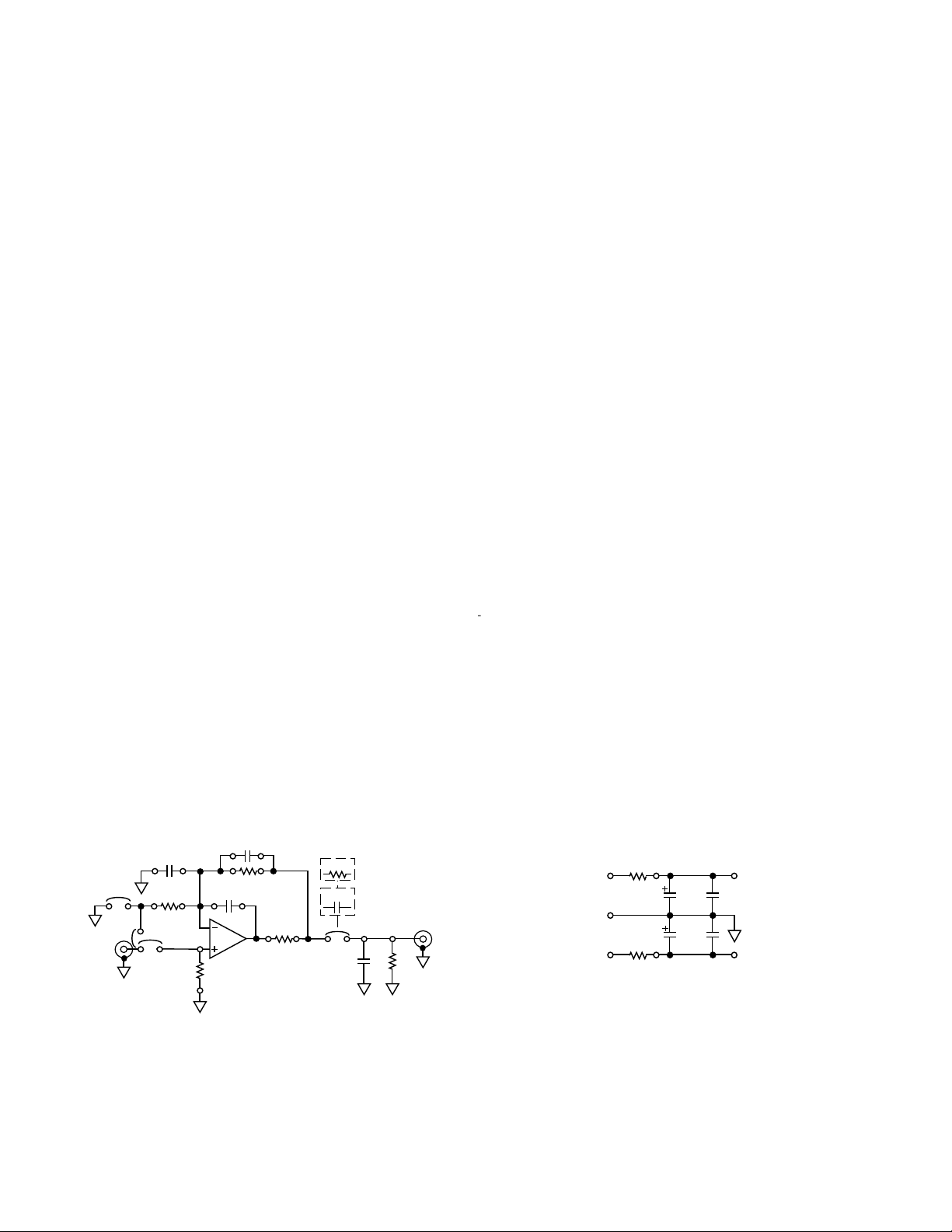
Figure 1 illustrates the basic circuit configuration for
each of the evaluation boards. Provisions have been
made to the board for optional components in addition
to the required feedback resistors and power supply bypass capacitors. For example, if the application requires
evaluating amplifier inside-the-loop capacitive load
compensation, then R
nal outside-the-loop compensation technique is used, a
jumper is substituted for R
C1
J1
V
IN
R1
J3
J2
R3
and CX can be used. If an exter-
X
, CX is removed completely,
X
C2
R4
R2
C
X
R
X
C3
J4
C
L
•
by Adolfo A. Garcia, Manager
ADSC Applications Engineering
V
R
L
APPLICATION NOTE
NORWOOD, MASSACHUSETTS 02062-9106
and R4 is inserted in series with the amplifier output.
Jumpers and open circuits are used throughout the
evaluation board as necessary to provide most any
circuit configuration. For example, if the application
requires an ac-coupled output voltage, then C3 can be
substituted for J4.
Power Supply Connections
Power supply connections for the evaluation boards are
shown in Figure 2. For optimal low frequency power
OUT
supply filtering, C
electrolytic capacitors. These capacitors should be of
the tantalum type with working voltages greater
than 25 V in ±15 V applications. C
ceramic capacitors and are located in close proximity to
the amplifier’s supply pins for optimal high frequency
filtering. They, too, should exhibit working voltages
greater than or equal to 25 V. For additional filtering,
provisions have been made for the use of resistors in
series with the amplifier power supply leads (R
R
). To avoid input/output voltage headroom issues,
S–
voltage drops due to these resistors should be limited to
less than 0.1 V. If these resistors are not needed, then
0.4” wire jumpers should be used.
V+
GND
V–
and CP2 should be 10 µF (or larger)
P1
R
S+ PIN 7 (SINGLE)
C
C
P1
10µF
C
10µF
R
S–
P3
0.1µF
C
P4
P2
0.1µF
•
and CP4 are 0.1 µ F
P3
PIN 8 (DUAL)
PIN 4 (QUAD)
PIN 4 (SINGLE, DUAL)
PIN 11 (QUAD)
617/329-4700
and
S+
Figure 1. Complete Circuit Schematic and Connections
for the Operational Amplifier Evaluation Board
Figure 2. Power Supply Connections and Bypassing Components for the Operational Amplifier Evaluation Board
Noninverting and Inverting Amplifier Configurations
Configuring the evaluation board for noninverting
amplifier applications is straightforward and is shown in
Figure 3. In this configuration, jumper J1 connects R1 to
GND, jumper J2 couples the input signal to the
noninverting terminal of the amplifier, C
together, and jumper J3 is substituted for R
is removed al-
X
. R3 can be
X
used as a termination/input bias current compensation
resistor, if required. The circuit‘s signal transfer equation, including the effects of finite amplifier open-loop
gain, is given by Equation 1:
R
2
R
1
Eq. 1
where
V
OUT
=1+
V
IN
A
= Amplifier open-loop gain, in Volts per
OL
R
2
R
1
1+
1
1
1+
A
OL
Volt (V/V);
and
R2, R1
= Amplifier feedback network resistors,
in ohms
C1
J1
V
IN
R1
J2
R3
C2
R2
J3
J4
R
L
V
OUT
Filter capacitors C2 and C1 can be used to tailor the response of the amplifier circuit. For either noninverting
or inverting applications, capacitor C2 works with R2 to
bandlimit the amplifier’s high frequency response and
places a pole in the response at:
2π×
1
R2×C
2
f
=
P
Eq. 3
On the other hand, capacitor C1 works with R1 to introduce a zero in the amplifier response. The location of
this low frequency corner is given by Equation 4:
2π×
1
R1×C
1
f
=
Z
Eq. 4
Note, capacitor C1 should be used only in noninverting
amplifier configurations, for, if it were used in inverting
amplifier applications, it would appear in parallel with
the input capacitance of the operational amplifier and
could cause instability.
In many applications, it is often necessary to evaluate
the total output voltage error of an amplifier configuration due to amplifier input offset voltage, commonmode rejection, input bias and offset currents, and
open-loop gain. Using either the noninverting or the inverting amplifier configuration, the total output voltage
error of an amplifier due to these parameters is given by
Equation 5:
V
OUT
=
1+
1
1
1+
()
A
OL
R
R
2
1
×
Figure 3. Circuit Configurations for Noninverting Amplifier Applications
For inverting amplifier applications, the circuit configuration is shown in Figure 4. The input signal is applied to
R1 through J1; thus, the circuit’s transfer equation is
given by Equation 2:
where A
V
IN
=−
R
R
2
1
1+
A
C2
R2
1
1
1+
()
OL
J2
V
OUT
V
IN
, R2, and R1 have been previously defined.
OL
R1
J1
R3
R
R
2
1
Eq. 2
J3
R
L
V
OUT
Figure 4. Circuit Connections for Inverting Amplifier
Applications
V
V
OS
()
[]
where
CM
+
CMRR
A
= Amplifier open-loop gain, in V/V;
OL
V
= Amplifier input offset voltage, in volts;
OS
V
= Applied input common-mode voltage,
CM
R
2
1+
()
R
1
I
OS
+
I
−
×
R
B
()
2
2
Eq. 5
in volts;
CMRR
= Amplifier common-mode rejection
ratio, in V/V;
I
= Amplifier input bias current, in amperes;
B
I
= Amplifier input offset current, in amperes;
OS
and
R2, R1
= Amplifier feedback network resistors,
in ohms.
In applications where large source/feedback resistors or
amplifiers with large input bias currents are used, then
R3 should be set to the parallel combination of R1 and
R2.
–2–

Amplifier Capacitive Load Compensation
As with any operational amplifier, care must be taken
when driving capacitive loads. Many operational amplifier data sheets now provide information with regard to
amplifier output voltage overshoot versus capacitive
load. In those cases where little or no information is
provided by the manufacturer on this issue, the circuit
configuration shown in Figure 5 can be used to evaluate
an amplifier’s capacitive load driving capability using an
inside-the-loop compensation technique. This technique
works equally well for inverting or noninverting applications where the closed-loop circuit gain is greater than
unity. Unity-gain circuit configurations for inside-theloop capacitive load compensation are a special case
and will be mentioned shortly.
R2
J1
J2
V
IN
R1
J3
C
X
R
X
R3
J4
C
L
V
OUT
Figure 5. Amplifier Circuit Connections for an Inside-theLoop Capacitive Load Compensation Technique
Load capacitance reacts with an amplifier’s open-loop
output resistance (R
) to produce an additional pole in
O
the feedback path. If the additional pole falls within the
loop-gain response of the amplifier, then the added
phase shift produced by this pole will introduce
response ringing and can even cause oscillation.
As shown in the figure, R
amplifier‘s output stage from the capacitive load, and C
is used to isolate the
X
X
is used to provide a secondary bypass feedback loop
which controls of the amplifier’s loop-gain response at
high frequencies. Although the selection for R
and C
X
X
is empirical in the final analysis, Equations 6 and 7 can
be used to select initial values for R
R
×R1
O
=
X
R
2
R
2 +R1
×
2
R
2
where
R
= 1+
C
X
R
1
A
CL
= Amplifier high-frequency, open-loop out-
O
×
C
and CX:
X
×
R
L
O
Eq. 6
Eq. 7
put resistance, in ohms;
A
= Amplifier closed-loop gain, in V/V;
CL
C
= Load capacitance, in farads;
L
and
R1, R2
= Amplifier feedback network resistances,
in ohms.
These equations are valid for either inverting or noninverting applications. Note, that R
(amplifier open-
O
loop output resistance) can be determined empirically
or from amplifier data sheets. If graphs for amplifier
output impedance versus frequency are provided, then
R
is equal to the value of the amplifier’s closed-loop
O
output impedance at the open-loop, unity-gain crossover frequency. Note, C
is a product of the circuit’s
X
closed-loop gain, the amplifier’s high frequency output
impedance, and the load capacitance.
Two important points with regard to this technique
require mention: First, R
large because the voltage drop across R
cannot be made arbitrarily
X
detracts from
X
the amplifier’s output voltage range. Second, this technique reduces the bandwidth of the circuit and is determined by Equation 8:
2π×
1
R2×C
X
Eq. 8
=
f
3
dB
Unity-gain noninverting amplifier applications are a
special case. Since R1, shown in Figure 5, is not used in
voltage buffer applications, Equation 7 cannot be used
to determine an initial value for C
approximation can be made for C
. In these cases, an
X
and is given by Equa-
X
tion 9:
R
×
C
X
L
R
2
Eq. 9
where
RX = R
2 ×
C
=
X
,
C
, and R2 have been previously defined.
O
L
In applications where an inside-the-loop compensation
technique cannot be used, as in the case for currentfeedback operational amplifiers, outside-the-feedback
loop compensation techniques substitute R4 for the
jumper wire at the output of the amplifier, as shown in
Figure 6. Note, capacitor C
a jumper wire is used in place of R
is removed completely and
X
. The value for R4 is
X
empirical, as it depends on the choice of amplifier,
capacitive load, and the closed-loop circuit gain. Some
amplifier data sheets (References [1] and [2]) provide
information regarding outside-the-loop capacitive load
compensation for those specific devices. However, in
general, drawbacks to this approach are: limited available slew rate (amplifier short-circuit current determines
output voltage slew rate), output voltage swing limitations (R4 forms a signal attenuator with R
bandwidth limitations (R4 and R
with C
).
L
form a low-pass filter
L
), and signal
L
–3–

R2
J1
V
IN
R1
J3
J2
R3
J4
R4
C
R
L
L
V
OUT
Figure 6. Amplifier Circuit Connections for an Outsidethe-Loop Capacitive Load Compensation Technique
Evaluation Board Application Caveats
These evaluation boards were designed for engineering
evaluations of single, dual, and quad operational
amplifiers. As such, these boards were intended for
engineering laboratory environments where ambient
temperatures range from +20 °C to +50°C. They are not
designed for heavy-duty production or incoming device
qualification where these boards could be exposed to
wide operating temperatures. In fact, since the layouts
of the circuits are not isothermal, their use in evaluating
operational amplifier input offset voltage drift performance over temperature should be carefully considered.
resonant-tuned circuits, components used in the evaluation board should have short leads, no longer than that
required for insertion directly into the board or into the
pin sockets. Lead forming tools are useful to help keep
resistor component lead lengths short: a lead 0.1” long
can exhibit a self-inductance of 2 nH.
Component labels on the Rev. 1 evaluation board silkscreens do not correspond with the component labels
shown in Figure 1. Their equivalencies to Figure 1 are:
R
= R1, RF = R2, RB = R3, CC = C1, CF = C2, RO = RX, R/C =
G
R4/C3. Capacitors C
, CP2, CP3, and CP4 on the Rev. 1
P1
evaluation boards are not labeled.
As previously mentioned, the evaluation board layouts
have not been optimized for high speed voltage- or current-feedback amplifiers that exhibit gain-bandwidth
products (GBWP) > 10 MHz. On the other hand, these
boards can be used in applications where signal rates of
change are less than 50 V/ µs.
Lastly, these boards should also not be used to evaluate
very low input bias current (I
< 50 pA) and electrometer-
B
grade operational amplifiers that require very clean
printed circuit boards, Teflon component standoffs, and
conformal coatings to minimize parasitic leakage
currents.
Circuit Board Layout and Construction Considerations
Figures 7, 8, and 9 illustrate the layouts of the single,
dual, and quad operational amplifier evaluation boards.
Although not shown to scale, the finished dimensions of
the boards are 4 inches by 3 1/8 inches for the single op
amp evaluation board, 4 3/16 inches by3 1/2 inches for
the dual op amp evaluation board, and4 3/4 inches by
4 5/8 inches for the quad op amp evaluation board. In
Figure 1, jumper wires J1, J2, and J3 are mounted into
the board on a 0.3” center-to-center spacing (“centers”),
and jumper wire J4 is mounted on 0.4” centers. Resistors used in the evaluation board should be of the metalfilm type and are mounted into the board on 0.4”
centers. Signal filter capacitors, C1 and C2, and supply
bypass capacitors, C
and CP4, are mounted into the
P3
evaluation board on 0.2” centers. Low frequency bypass capacitors, C
and CP2, are mounted into the
P1
boards on 0.1” center-to-center spacing.
Pin sockets are flush-mounted into the board, for ease of
component interchangeability. They are, however,
optional in those applications where higher speed
performance is necessary. To avoid unintentional
Figure 7a. Single Op Amp Evaluation Board Topside
Silkscreen (Not to Scale)
Figure 7b. Single Op Amp Evaluation Board Topside
Metalization (Not to Scale)
Figure 7c. Single Op Amp Evaluation Board Backside
Metalization (Not to Scale)
–4–

Figure 8a. Dual Op Amp Evaluation Board Topside
Silkscreen (Not to Scale)
Figure 9a. Quad Op Amp Evaluation Board Topside
Silkscreen (Not to Scale)
Figure 8b. Dual Op Amp Evaluation Board Topside
Metalization (Not to Scale)
Figure 8c. Dual Op Amp Evaluation Board Backside
Metalization (Not to Scale)
Figure 9b. Quad Op Amp Evaluation Board Topside
Metalization (Not to Scale)
Figure 9c. Quad Op Amp Evaluation Board Backside
Metalization (Not to Scale)
–5–

An example of a complete evaluation board is illustrated
in Figure 10. The circuit is constructed around the
OP279, a single-supply, rail-to-rail input/output operational amplifier with high output current drive. Each of
the amplifiers in the circuit was configured for a gain of
+10 using 909 Ω for R2 and 100 Ω for R1.
Figure 10. Dual Op Amp Evaluation Board Configured for
the OP279 in a Gain-of-10 Noninverting Application
Acknowledgments
The author wishes to acknowledge the efforts of Louis
Agot, PRA engineering technician, who designed the
board layouts, routed, built, and tested the prototypes.
Operational Amplifier Evaluation Board Materials List
For the single operational amplifier evaluation board:
Description Quantity
For the dual operational amplifier evaluation board:
Description Quantity
Evaluation Board 1
Pin Sockets 60
BNC Connectors, Female 4
Double Turret Terminals 3
8-Pin DIP Machine Socket (Optional) 1
For the quad operational amplifier evaluation board:
Description Quantity
Evaluation Board 1
Pin Sockets 114
BNC Connectors, Female 8
Double Turret Terminals 3
14-Pin DIP Machine Socket (Optional) 1
NOTES
1
All pin socket quantities include those required for the power supply
bypass components. Pin sockets are available from MIL-MAX (Part No.
0255-0-15-01-30-02-04-0). MIL-MAX can be contacted at (516) 922-6000.
2
BNC connectors can be either PC mount (Pomona P/N: 4578) or Right
Angle mount (Pomona P/N: 4788).
3
Double turret terminals can be purchased from Keystone (Part No. 1503)
or equivalent.
4
In those cases where machine sockets are used for the IC in the board,
pin socket quantities for the single, dual, and quad operational evaluation boards are 28, 52, and 100, respectively.
REFERENCES
1. ”AD9617 Low Distortion, Precision Wideband Operational Amplifier Data Sheet.” Order number: C1353–
10–10/89.
E2233–12–5/95
Evaluation Board 1
Pin Sockets
BNC Connectors, Female
Double Turret Terminals
8-Pin DIP Machine Socket (Optional)
1
2
3
4
36
2
3
1
2. “AD811 High Performance Video Operational Amplifier Data Sheet.” Order number: C1592–24–11/91.
These data sheets can be requested directly from the
Analog Devices Literature Center at (800) 262-5643,
Option 2, or at (617) 461-3392.
PRINTED IN U.S.A.
–6–
 Loading...