

Page 1
AN-392
a
ONE TECHNOLOGY WAY • P.O. BOX 9106
Circuit Design and Applications of the ADM663A/ADM666A
Micropower Linear Voltage Regulators
GENERAL INFORMATION
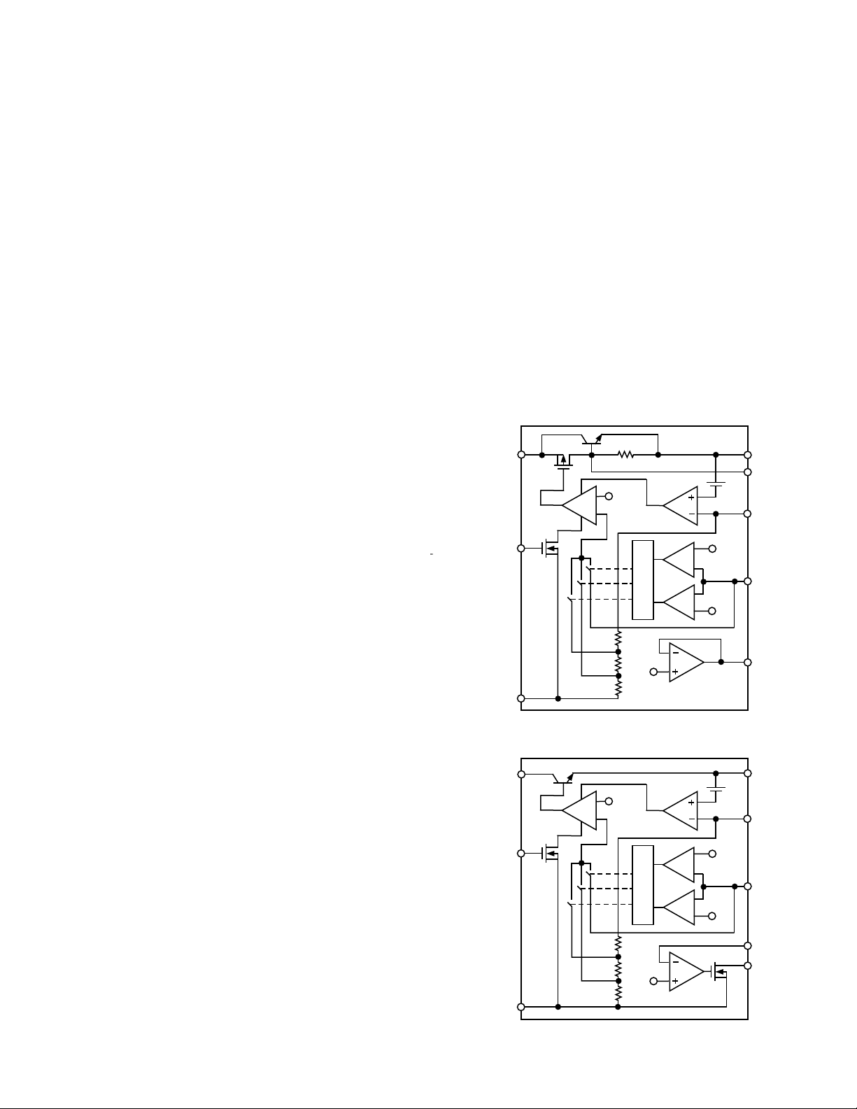
The ADM663A/ADM666A contains a micropower bandgap reference voltage source; an error amplifier, A1;
three comparators, C1, C2, C3, and a series pass output
transistor. A P-channel FET and an NPN transistor are
used on the ADM663A while the ADM666A uses an NPN
output transistor.
CIRCUIT DESCRIPTION
The internal bandgap reference is trimmed to 1.3 V
± 30 mV. This is used as a reference input to the error
amplifier A1. The feedback signal from the regulator output is supplied to the other input by an on-chip voltage
divider or by two external resistors. When V
ground, the internal divider tap between R1 and R2, provides the error amplifier’s feedback signal giving a +5 V
output. When V
tween R2 and R3 provides the error amplifier’s feedback
signal giving a +3.3 V output. When V
50 mV above ground and less than 50 mV below V
error amplifier’s input is switched directly to the V
pin, and external resistors are used to set the output
voltage. The external resistors are selected so that the
desired output voltage gives 1.3 V at V
Comparator C1 monitors the output current via the
SENSE input. This input, referenced to V
the voltage drop across a load sense resistor. If the voltage drop exceeds 0.5 V, then the error amplifier A1 is
disabled and the output current is limited.
The ADM663A has an additional amplifier, A2, which
provides a temperature proportional output, V
is summed into the inverting input of the error amplifier,
a negative temperature coefficient results at the output.
This is useful when powering liquid crystal displays over
wide temperature ranges.
The ADM666A has an additional comparator, C4, that
compares the voltage on the low battery input, LBI, pin
to the internal +1.3 V reference. The output from the
comparator drives an open drain FET connected to the
low battery output pin, LBO. The low battery threshold
is at VIN, the internal divider tap be-
SET
is at more than
SET
.
SET
OUT(2)
•
by Khy Vijeh, Matt Smith
is at
SET
, the
IN
, monitors
. If this
TC
APPLICATION NOTE
NORWOOD, MASSACHUSETTS 02062-9106
may be set using a suitable voltage divider connected to
LBI. When the voltage on LBI falls below 1.3 V, the open
drain output LBO is pulled low.
22k
1.3V
A1
D
E
C
O
D
E
R
R1
R2
0.9V
R3
1.3V
A1
D
E
C
O
D
E
R
R1
R2
1.3V
R3
SET
V
IN
SHDN
GND
Figure 1. ADM663A Functional Block Diagram
V
IN
SHDN
GND
Figure 2. ADM666A Functional Block Diagram
C1
VIN–50mV
C2
C3
50mV
A2
ADM663A
C1
VIN–50mV
C2
C3
50mV
C4
ADM666A
•
617/329-4700
V
OUT2
V
OUT1
0.5V
SENSE
V
SET
V
TC
V
OUT
0.5V
SENSE
V
SET
LBI
LBO
Page 2

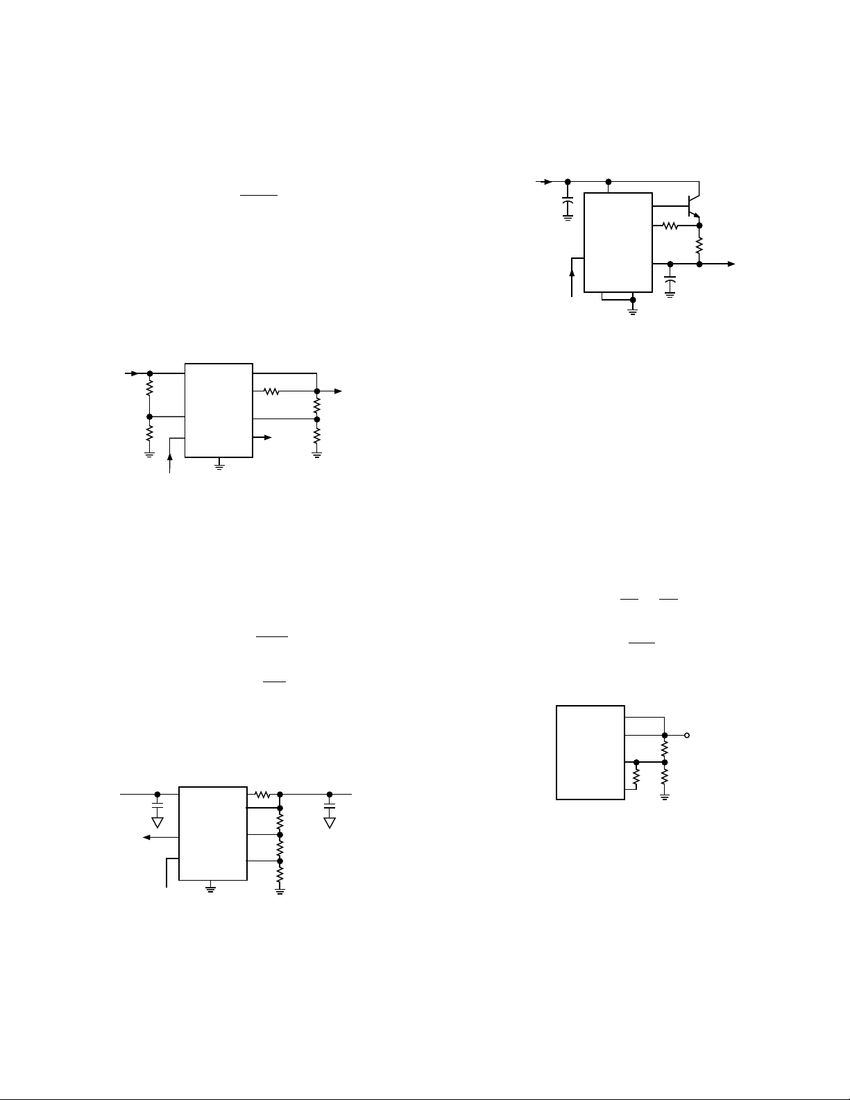
Both the ADM663A and the ADM666A contain a shutdown (SHDN) input that can be used to disable the error
amplifier and hence the voltage output. The power consumption in shutdown reduces to less than 9 µA.
Circuit Configurations
For a fixed +5 V output the V
input is grounded and no
SET
external resistors are necessary. This basic configuration is shown in Figure 3. For a fixed +3.3 V output, the
V
input is connected to VIN as shown in Figure 4. Cur-
SET
rent limiting is not being utilized so the SENSE input is
connected to V
+6V TO +16V
INPUT
OUT(2)
0.1µF
.
V
IN
ADM663A
ADM666A
V
SET
SENSE
V
OUT2
GND SHDN
0.1µF
+5V
OUTPUT
Figure 3. A Fixed +5 V Output
+4.5V TO +16V
INPUT
0.1µF
V
IN
ADM663A
ADM666A
V
SET
SENSE
V
OUT2
GND SHDN
0.1µF
+3.3V
OUTPUT
+2V TO +16V
INPUT
V
IN
ADM663A
ADM666A
SHDN
GND
SENSE
V
OUT2
V
SET
R
CL
+1.3V TO +15V
OUTPUT
R2
R1
Figure 5. Adjustable Output
Table I. Output Voltage Selection
V
SET
V
OUT
GND +5 V
V
IN
+3 V
R1/R2 ADJ
Current Limiting
Current limiting may be achieved by using an external
current sense resistor in series with V
OUT(2)
. When the
voltage across the sense resistor exceeds the internal
0.5 V threshold, current limiting is activated. The sense
resistor is therefore chosen such that the voltage across
it will be 0.5 V when the desired current limit is reached.
0.5
R
=
CL
I
CL
where RCL is the current sense resistor, ICL is the maximum current limit.
Figure 4. A Fixed +3.3 V Output
Output Voltage Setting
If V
is not connected to GND or to VIN, the output volt-
SET
age is set according to the following equation:
(
R1+R
2)
R
1
where V
= 1.30 V.
SET
V
=
V
OUT
SET
×
The resistor values may be selected by first choosing a
value for R1 and then selecting R2 according to the following equation:
V
R
2 =R1×
1. 3 0
The input leakage current on V
OUT
–1
is 10 nA maximum.
SET
This allows large resistor values to be chosen for R1 and
R2 with little degradation in accuracy. For example, a
1 MΩ resistor may be selected for R1, and then R2 may
be calculated accordingly. The tolerance on V
is guar-
SET
anteed at less than ±30 mV so in most applications, fixed
resistors will be suitable.
The value chosen for R
should also ensure that the cur-
CL
rent is limited to less than the 100 mA absolute maximum rating and also that the power dissipation will also
be within the package maximum ratings.
If current limiting is employed, there will be an additional voltage drop across the external sense resistor
that must be considered when determining the regulators dropout voltage.
If current limiting is not used, the SENSE input should
be connected to V
. In this case, input current should
OUT(2)
be limited so that in case of short circuited output,
device power dissipation does not exceed the rated
maximum.
Shutdown Input (SHDN)
The SHDN input allows the regulator to be turned off
with a logic level signal. This will disable the output and
reduce the current drain to a low quiescent (9 µA maximum) current. This is very useful for low power applications. The SHDN input should be driven with a CMOS
logic level signal since the input threshold is 0.3 V. In
TTL systems, an open collector driver with a pull-up resistor may be used.
If the shutdown function is not being used, then it
should be connected to GND.
–2–
Page 3
Low Supply or Low Battery Detection
The ADM666A contains on-chip circuitry for low power
supply or battery detection. If the voltage on the LBI pin
falls below the internal 1.3 V reference, then the open
drain output LBO will go low. The low threshold voltage
may be set to any voltage above 1.3 V by appropriate
resistor divider selection.
R
3 =R4
V
BATT
1. 3
–1
V
where R3 and R4 are the resistive divider resistors and
V
is the desired low voltage threshold.
BATT
Since the LBI input leakage current is less than 10 nA,
large values may be selected for R3 and R4 in order to
minimize loading. For example, a 6 V low threshold may
be set using 10 M Ω for R3 and 2.7 M Ω for R4.
+2V TO +16V
INPUT
V
SENSE
IN
R3
ADM666A
LBI
R4
SHDN
GND
V
V
OUT
SET
LBO
R
CL
LOW
BATTERY
OUTPUT
+1.3V TO +15V
OUTPUT
R2
R1
Figure 6. ADM666A Adjustable Output with Low
Battery Detection
Low Output Detection
The circuit in Figure 7 will generate a low LBO when output voltage drops below a preset value determined by
the following equations:
V
for V
R
2 +R3 =R1
R
3= (R1+R2)
= 5.0 V nominal, VOL = 3% of V
OUT
1. 3
V
OUT
OL
1. 3
–1
–1
= 4.85 V and R1
OUT
= 1 MΩ solving the equations simultaneously we will get
R2 = 31 k Ω and R3 = 2.82 M Ω.
V
= 5V
OUT
0.1µF
0.1µF
V
IN
LBO
SHDN
GND
V
OUT
SENSE
LBI
V
SET
R3
2.82MΩ
R2
31kΩ
R1
1MΩ
High Current Operation
The ADM663A contains an additional output, V
OUT1
, suitable for directly driving the base of an external NPN
transistor. Figure 8 shows a configuration which can be
used to provide +5 V with boosted current drive. A 1 Ω
current sensing resistor limits the current at 0.5 A.
V
IN
+
10µF
SHUTDOWN
V
IN
ADM663A
SHDN
GND
V
SET
V
OUT1
V
OUT2
SENSE
100Ω
+
10µF
2N4237
1.0Ω
+5V, 0.5A
OUTPUT
Figure 8. ADM663A Boosted Output Current (0.5 A)
Temperature Proportional Output
The ADM663A contains a VTC output with a positive temperature coefficient of +2.5 mV/ °C typ. This may be connected to the summing junction of the error amplifier
(V
) through a resistor resulting in a negative tempera-
SET
ture coefficient at the output of the regulator. This is
especially useful in multiplexed LCD displays to compensate for the inherent negative temperature coefficient of the LCD threshold. At +25 °C, the voltage at the
VTC output is typically 0.9 V. The equations for setting
both the output voltage and the tempco are given below. If this function is not being used, then V
should be
TC
left unconnected.
R
2
R
2
(
V
–
V
+
1
–
R
2
R
3
R
3
(
TCV
R2
R1R3
TC
SET
V
OUT
)
TC
)
where V
V
=
OUT
V
1+
SET
R
TCV
= +1.3 V, VTC = +0.9 V, TCVTC = +2.5 mV/ °C
SET
ADM663A
OUT
SENSE
V
OUT2
V
SET
V
=
TC
Figure 9. ADM663A Temperature Proportional Output
Figure 7. Voltage Regulator Circuit with Low Output
Detector
–3–
Page 4

APPLICATION HINTS
Input-Output (Dropout Voltage)
A regulator’s minimum input-output differential or
dropout voltage determines the lowest input voltage for
a particular output voltage. The ADM663A/ADM666A
dropout voltage is 1 V at 100 mA output current. For
example when used as a fixed +5 V regulator, the minimum input voltage is +6 V. At lower output currents
(I
< 10 mA) on the ADM663A, V
OUT
may be used as
OUT1
the output driver in order to achieve lower dropout voltages. In this case the dropout voltage depends on the
voltage drop across the internal FET transistor. This may
be calculated by multiplying the FET’s saturation resistance by the output current, for example with V
R
= 20 Ω. Therefore, the dropout voltage for 5 mA is
SAT
= 9 V,
IN
100 mV. As the current limit circuitry is referenced to
V
, V
OUT2
should be connected to V
OUT2
rent operation V
should be used alone and V
OUT2
. For high cur-
OUT1
OUT1
left
unconnected.
P
= Power Dissipation (W)
D
θJA = Junction to Ambient Thermal Resistance ( °C/W)
If the device is being operated at the maximum permitted ambient temperature of +85 ° C, the maximum power
dissipation permitted is:
PD (max
) = (
TJ (max
P
(
max
D
) = (125 – 85)/(θJA)
= 40/θ
) –
T
)/(θJA)
A
JA
θJA = 120°C/W for the 8-pin DIP (N-8) package
θ
= 170°C/W for the 8-pin SOIC (R-8) package
JA
Therefore, for a maximum ambient temperature of 85 °C
P
(
max
) = 333
D
P
(
max
) = 235
D
mW for N
mW for R
-8
-8
+6V TO +16V
INPUT
V
V
IN
ADM663A
GND SHDN
SET
SENSE
V
OUT2
V
OUT1
+5V
OUTPUT
Figure 10. Low Current, Low Dropout Configuration
Thermal Considerations
The ADM663A/ADM666A can supply up to 100 mA load
current and can operate with input voltages up to 16.5 V,
but the package power dissipation and hence the die
temperature must be kept within the maximum limits.
The package power dissipation is calculated from the
product of the voltage differential across the regulator
times the current being supplied to the load. The power
dissipation must be kept within the maximum limits
given in the Absolute Maximum Ratings section.
PD
= (
VIN–V
OUT
) (
I
)
L
The die temperature is dependent on both the ambient
temperature and on the power being dissipated by the
device. The ADM663A/ADM666A contains an internal
thermal limiting circuit which will shut down the regulator if the internal die temperature exceeds 125 °C. Therefore, care must be taken to ensure that, under normal
operating conditions, the die temperature is kept below
the thermal limit.
T
=
J
TA + PD
(θJA)
This may be expressed in terms of power dissipation as
follows:
PD = (TJ – T
)/(θJA)
A
where:
T
= Die Junction Temperature ( °C)
J
T
= Ambient Temperature ( °C)
A
At lower ambient temperatures the maximum permitted
power dissipation increases accordingly up to the
maximum limits specified in the absolute maximum
specifications.
The thermal impedance ( θ
) figures given are mea-
JA
sured in still air conditions and are reduced considerably where fan assisted cooling is employed. Other
techniques for reducing the thermal impedance include
large contact pads on the printed circuit board and wide
traces. The copper will act as a heat exchanger thereby
reducing the effective thermal impedance.
High Power Dissipation Recommendations
Where excessive power dissipation due to high
input-output differential voltages and or high current
conditions exists, the simplest method of reducing the
power requirements on the regulator is to use a series
dropping resistor. In this way the excess power can be
dissipated in the external resistor. As an example, consider an input voltage of +12 V and an output voltage
requirement of +5 V @ 100 mA with an ambient temperature of +85 °C. The package power dissipation under
these conditions is 700 mW which exceeds the maximum ratings. By using a dropper resistor to drop 4 V,
the power dissipation requirement for the regulator is
reduced to 300 mW which is within the maximum specifications for the N-8 package at +85 °C. The resistor value
is calculated as R = 4/0.1 = 40 Ω. A resistor power rating
of 400 mW or greater may be used.
Bypass Capacitors
The high frequency performance of the ADM663A/
ADM666A may be improved by decoupling the output
using a filter capacitor. A capacitor of 0.1 µF is suitable.
An input capacitor helps reduce noise, improves dynamic performance and reduces the input dV/dt at the
regulator input. A suitable input capacitor is 0.1 µF or
greater.
–4–
Page 5

Typical Performance Characteristics
80
60
40
PSRR – dB
20
0
0.01 0.1 100001000100101
FREQUENCY – Hz
VINDC = +9V
V
p-p = +2V
IN
V
DC = +5V
OUT
TA = +25°C
Figure 11. Power Supply Rejection Ratio vs. Frequency
2.0
1.8
1.6
1.4
1.2
) – Volts
1.0
OUT
0.8
– V
IN
(V
0.6
0.4
0.2
0
2
0
VIN = +2V
I
OUT1
– mA
TA = +25°C
VIN = +9V
VIN = +15V
1816141210864
20
2.0
1.8
1.6
1.4
1.2
– Volts
1.0
OUT
0.8
– V
IN
V
0.6
0.4
0.2
0.0
Figure 14. ADM663 V
TA = +25°C
663A/666A
V
VIN = +2V
V
IN
0 12020 40 60 80 100
IN
= +15V
I
– mA
OUT
, ADM666 Input-Output
OUT2
Differential vs. Output Current
C2 = 10µF
V
= 9V
IN
10µF
V
IN
C2 = 1µF
C2
= +9V
SCOPE
80Ω
0-4V
Figure 12. ADM663A V
Input-Output
OUT1
Differential vs. Output Current
12
TA = +25°C
10
8
6
– µA
IN
I
4
2
0
2 4 6 8 10 12 14 16
V
IN
– Volts
V
V
OUT
OUT
= +5V
= +3.3V
Figure 13. Quiescent Current vs. Input Voltage
50mV
200µs
Figure 15. Load Transient Response
2.0A LDO Voltage Regulator with Short Circuit Protection
In battery powered systems, battery life is significantly
affected by the voltage regulator’s dropout voltage.
These systems often require low dropout linear regulators capable of high output current and extremely low
quiescent current.
The circuit in Figure 16 can source current in excess of
2 A with less than 400 mV dropout voltage and consumes less than 10 µA in shutdown mode. The c ircuit
exhibits excellent line and load regulation and better
than 5% initial output voltage accuracy.
Unlike other LDO voltage regulators which require large
capacitors in excess of 10 µF for stability, a very small
0.1 µF bypass capacitor is sufficient for this circuit.
–5–
Page 6

VIN = 5.5
1µF
2N6111
R3
+
1kΩ
–
Q1
8
V
IN
V
SET
R1
28kΩ
1%
6
ADM666A
5
SHDN
GND SENSE
41
2
V
OUT
R4
5Ω
R2
9.5kΩ
1%
5V @ 2A
0.1µF
Figure 16. 2.0A LDO Regulator
The circuit’s maximum current is determined by the
selection of the pass transistor’s current gain, ß, and its
maximum power dissipation. For low dropout voltage, a
viable choice is a PNP pass transistor with appropriate
power dissipation and ß. The s implified functional diagram in Figure 17 helps clarify the circuit’s operation.
V
IN
1µF
1.3V
R3
1kΩ
A1
2N6111
86
Q2
Q1
28kΩ
R1
R2
9.5kΩ
0.1µF
For high current applications where low dropout voltage
is not required, a power Darlington transistor can be
substituted to take advantage of its relatively high ß.
The trade-off of this approach is higher power dissipation due to Darlington’s high saturation voltage.
Output voltage is programmable between 1.3 V to 15.4 V
by selecting appropriate resistor values for the voltage
divider network using the following equation:
=1. 3
V
V
OUT
R
2
R
1 +R2
The circuit’s performance is shown in Figures 18 and 19.
5.050
5.000
4.950
4.900
OUT
V
OUT
V
4.850
4.800
4.750
5.0 7.05.2 5.4 5.6 5.8 6.0 6.2 6.4 6.6 6.8
5.0036
4.990
V
IN
0.0136
RL = 2.05Ω
ADM666
4
21
R4
5Ω
Figure 17. Simplified Functional Diagram
The 2N6111 is in a servo loop with ADM666A’s voltage
reference, error amplifier and driver circuit.
To maintain regulation, output voltage is continuously
monitored by comparing the voltage on the set pin
(Pin 6) to a 1.3 V internal voltage reference. The difference is amplified by the error amplifier, A1, and used to
control the pass transistor’s base current, thus controlling its collector current. As output voltage changes due
to a change in input voltage or load current, the pass
transistor’s base current is adjusted to maintain a constant output voltage.
Since maximum base current is limited to ADM666A’s,
short circuit current set by R4 to 100 mA, pass transistors with higher ß will source higher currents to the
load. As a result, output short circuit current behavior of
the circuit depends on the pass transistor’s ß.
Another significant advantage of using a pass transistor
with high ß is to achieve higher efficiency since most of
the input current is diverted to the load and only a small
fraction of it is used to control the servo loop.
Figure 18. Output Voltage vs. Input Voltage
0
5
10
15
20
– VARIATION – mV
OUT
V
25
30
0
0.2 0.4 0.6
I
LOAD
– A
0.8
1.0
1.5
2.0 3.0
Figure 19. Output Voltage Variation vs. Load Current
The short circuit current is limited by limiting the pass
transistor’s base current, I
to a value determined by:
b
0.5
I
=
b
R
4
The actual value of the short circuit current is determined by the ß of the pass transistor which in this case
is in 30 to 150 range at a collector current of 3.0 A dc.
For more accurate short circuit current control, the
circuit in Figure 20 is a simple way to add short circuit
protection.
–6–
Page 7

1µF
2x
2N3906
20Ω
RSC = 0.05Ω
50kΩ
750kΩ
850Ω
1N4728
3.3V, ZENER
2kΩ
ADM666
5
SHDN
GND SENSE
2N6111
V
IN
4
R1
8
28kΩ
6
V
SET
R2
2
V
OUT
1
9.5kΩ
R4
5Ω
Figure 20. External Short Circuit Protection
The short circuit current is determined by using the
following equation:
0.1
R
=
SC
I
SC
An appropriate heat sink must be utilized to avoid damage to the pass transistor as well as controller IC. Figure
21 is a plot of the current through the controller and voltage across it vs. input voltage at a constant load current.
As the curve indicates, maximum power dissipation for
controller occurs when input voltage is between 5.4 V to
5.6 V, worst case being 215 mW at V
= 5.53 V, which is
IN
well within the product specification.
0.1µF
An N-channel power FET switch with very low RON is
used to achieve a very low dropout across the switch
when it is ON.
Optional resistor R3 is used to compensate for constant
losses by self-discharge or trickle charging of the battery. Consult the battery specification to determine
trickle charge current and maximum permissible over
charge current.
Resistor values used in this circuit are optimized for low
power operation, when monitoring BAT-ON output;
avoid excessive loads on this output.
Shut-down pin should be tied to ground if it is not used.
BAT ON
0.1µF
3.3V
100mA
R1
7.31MΩ
R2
2.5MΩ
SHUTDOWN
D1
VP12A
R3
8
V
IN
6
V
7
3
SET
LBO
ADM666A
LBI
GND
4 5
1µF
6V
100kΩ
50kΩ
150kΩ
V
OUT
SENSE
SHDN
2
1
mA
130
110
I
B
I
B
V
90
70
50
30
10
IN
I
8
ADM666
2
5Ω
5.0 7.05.2 5.4 5.6 5.8 6.0
RL = 2.05Ω
V
8–2
V
215 mW
V
IN
5.0
4.8
4.6
4.4
4.2
4.0
3.8
Figure 21. Controller IC Power Dissipation
However, the pass transistor requires adequate heat
sink specially if it were to operate with large input output
voltage differential.
LDO Regulator with Battery Crossover Switch
The circuit in Figure 22 automatically connects the
standby battery to the circuit when primary voltage
source is disconnected or drops below a preset voltage
level.
Battery ON voltage level is determined using the following equation:
R1=R
(
V
BAT
2
1. 3
)
–1
V
Figure 22. LDO Regulator with Battery Crossover
Switch Circuit
Low Battery Disconnect Circuit
To prevent damage to the battery and loss of data due to
battery over-discharge, the circuit illustrated in Figure
23 monitors the battery voltage and disconnects the battery from the circuit when it drops below a preset value.
VOLTAGE ACROSS PINS 8 AND 2
6V SEALED LEAD-ACID
BATTERY SOURCE
6V
Figure 23. Low Battery Disconnect and Memory
Backup Circuit
Diode D2 is added for isolation; D1 is to compensate for
voltage drop across D2. For better output voltage accuracy performance, diodes D1 and D2 must be in thermal
contact. Surface mount Schottky diodes mounted in
close proximity of each other offer the best temperature
tracking performance.
8
V
+
R1
6.54MΩ
600kΩ
R2
2.5MΩ
FOR BEST TEMPERATURE TRACKING PERFORMANCE,
*
DIODES MUST BE IN THERMAL CONTACT.
1µF
R4
2MΩ
2N2222
9.1MΩ
R5
R3
6
V
3
LBI
5
7
LBO
IN
SET
SHDN
ADM666A
V
OUT
SENSE
2
1
D1
0.1µF
MAIN
D2
*
V+
MEMORY
*
D3
V+
R6
10Ω
LBO
–7–
Page 8
In battery disconnect mode, the circuit’s quiescent current is less than 20 µA. If LBO function is not needed or it
is monitored via a high impedance input, the circuit’s
current consumption can be reduced significantly by replacing R4 with a short and R3 with a 9 M Ω resistor. This
circuit has less than 10 µA quiescent current.
5 Volt Supply with Battery Backup and Battery ON Lag
The circuit in Figure 24 switches to NiCd backup battery
when the main input voltage drops below value set by
R1, R2 and R3 and returns to the main input when its
voltage reaches the preset value set by R3.
V
OUT
SENSE
LBO
2
1
100kΩ
7
51kΩ
MAIN 5V
MEMORY 5V
0.1µF
VP12A
1µF
8
V
+
R2
IN
R1
ADM666A
3
LBI
Charge termination voltage, VT, and charge resume voltage, V
nated when battery voltage reaches V
, are set by R3, R4 and R5. Charging is termi-
CH
.
T
Charge termination voltage, which in this case is 7.2 V,
is calculated using the following equation:
V
R
4 = (R5 +R6)
1. 3
T
–1
where R6 = 20 k Ω, and R4 = 9.2 M Ω.
ADM666A continues to monitor the battery voltage
level; charging will resume when it drops below the V
CH
The VCH level is set by adjusting R3.
With resistor values selected in Figure 26, charging
starts when the battery voltage is around V
= 5 volts
CH
and will terminate when the battery voltage reaches
slightly above 7.2 V.
.
E2032–12–5/95
150kΩ
5V NICD
BACKUP
+
–
LOW BATTERY
FLAG
SHOULD BE
CONNECTED
TO GND
IF NOT USED
5
SHDN
V
GND
SET
4
6
R3
HYST ADJ
Figure 24. 5 V Battery Powered Supply with Backup
and Battery ON Flag
The Battery ON flag goes low whenever the circuit is
switched to NiCd battery.
Low Cost Battery Charger Circuits
A simple, low cost and yet flexible battery charger is presented in Figure 25. Maximum output voltage is programmed by selection of R1 and R2 ratio’s using
V
for V
(
R1=R
= 7.8 V, R1 = 2.82 M Ω, and R2 = 560 k Ω. Maxi-
OUT
OUT
2
1.3
)
–
1
V
mum charge current is determined by the current limiting resistor which in this case is 100 mA set by R8.
R8 5Ω
2
V
= 9V
V
IN
+
1µF
8
V
R7
3k
5
SHDN
IN
SENSE
ADM666A
V
LBO
GND
4
OUT
SET
LBI
1
3
6
7
0.1µF
R3
270kΩ
R1 2.82MΩ
9.2MΩ
R2 560kΩ
R5
2MΩ
R6
20kΩ
CELLS
R4
Charger status is indicated by the LED. A lighted LED
indicates charger ON; a flashing LED indicates battery
disconnect.
To minimize calculation errors and maximize the circuit
efficiency, LED current should be limited to about 2 mA.
To minimize current drain by battery voltage monitoring
circuit’s, large resistor values are selected for R4 and R5
(see text for recommended values).
Charge current is limited to 100 mA by a short circuit
current limiting resistor. However higher charge current
is possible using the circuit in Figure 26.
V
IN
A1
SHDN
5
GND
22k
1.3V
R1
R2
0.9V
R3
C1
D
E
C
O
D
E
R
C2
C3
A2
ADM663A
VIN–50mV
50mV
0.5V
V
OUT2
V
OUT1
SENSE
V
SET
V
TC
Figure 26. High Charge Current Battery Charger
Power PNP pass transistor with appropriate current rating is controlled by the ADM666A.
Available charge current is determined by the
PRINTED IN U.S.A.
transistor’s power rating, its current gain, ß, and controlled by the short circuit current limit resistor.
Figure 25. Low Cost Battery Charger
–8–
 Loading...