Page 1

AN-380
a
ONE TECHNOLOGY WAY • P.O. BOX 9106
Compensating for the 0 g Offset Drift
of the ADXL50 Accelerometer
by Charles Kitchin and Paul Brokaw
INTRODUCTION
The ADXL50 accelerometer has a nominal sensitivity of
19 mV per g of applied acceleration. This is centered
around a +1.8 volt offset. The offset will typically drift
35 mV over a 0 to +70 °C temperature range. This drift is
very small compared with the amplitude of high g level
signals but becomes more significant as the measured
acceleration level decreases. For applications not needing a dc (i.e., gravity sensing) response, ac coupling between the preamplifier and the on-chip buffer amplifier
will eliminate almost all of the 0 g drift. But, in cases
where a dc response is needed, an external temperature
compensation circuit will greatly improve the low g performance of the accelerometer.
This application note shows how to compensate for the
linear component of the 0 g drift, using either a software
or a hardware approach.
•
APPLICATION NOTE
NORWOOD, MASSACHUSETTS 02062-9106
A Software Approach Using a µP Interface
For those applications where the ADXL50 output drives
a µP, it can be used to subtract out the 0 g drift over temperature. This can be indirectly approximated by using
the formula:
VOginmV
= ((1.3 × 10⁻⁵)
where T is the temperature in degrees centigrade, or by
directly digitizing the output of a temperature sensor,
using an ADC.
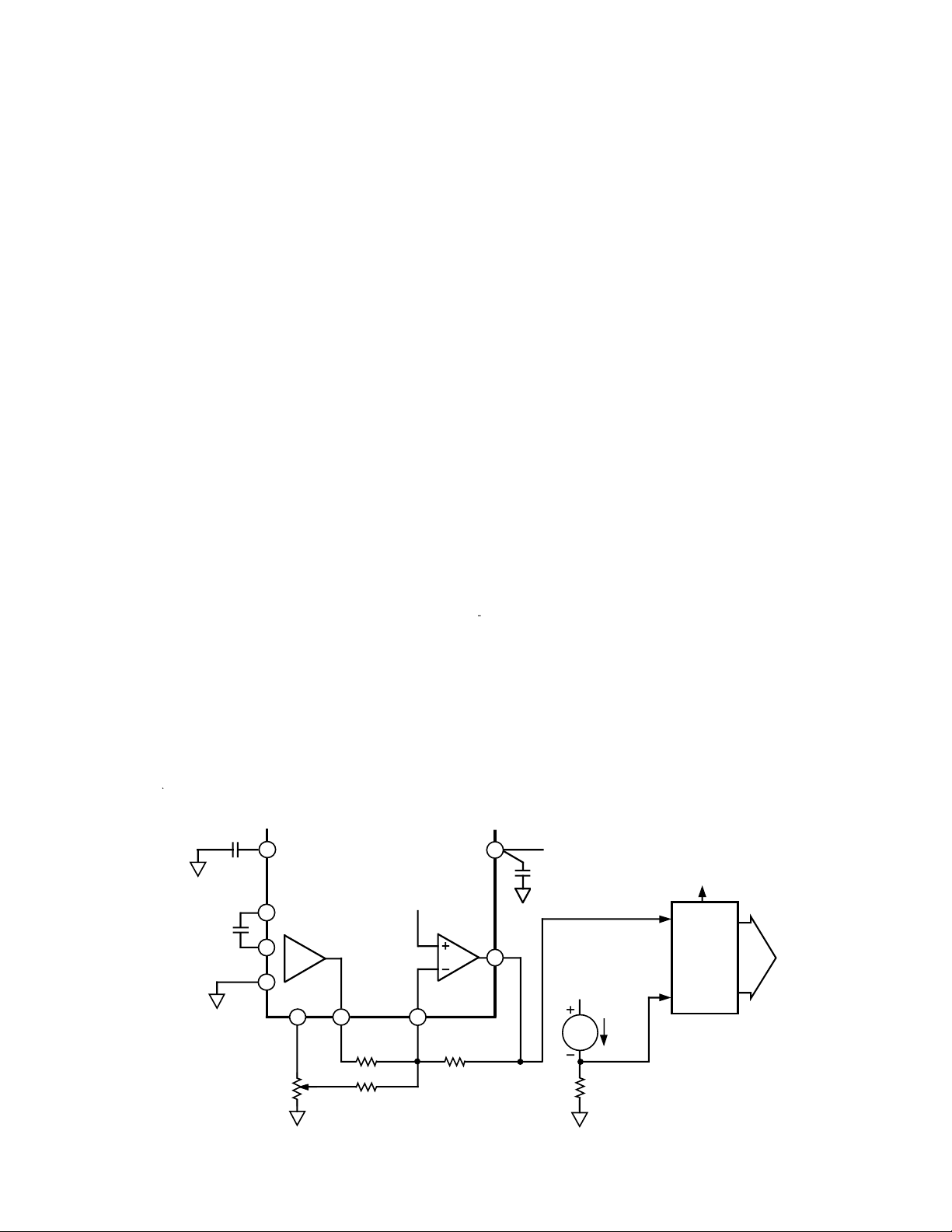
In the circuit of Figure 1, an AD590 temperature sensor
and a 1 k Ω resistor are added to the board containing the
accelerometer. The AD590 provides a 1 µA/°K current
output which, together with the 1 k Ω resistor, provides a
1 mV/°K output to the µP. For best temperature tracking,
the AD590 should be attached to the case of the ADXL50.
The outputs of the ADXL50 and the AD590 both run to
the µP. The circuit is then placed in an oven and operated over temperature; the µP then stores the drift curve
in its memory and subtracts it out for all succeeding
measurements.
3
T
) + ((2.3 × 10⁻³)
•
2
T
) – (0.08T) – 0.29
617/329-4700
0.022µF
0.022µF
0g LEVEL
ADJUST
C2
4 1
C1
2
PRE-AMP
3
C1
5
COM
6
+3.4V
REF
50kΩ
V
PR
ADXL50
8
49.9kΩ
100kΩ
1.8V
10
V
IN–
Figure 1. Acceleration & Temperature Outputs to µP
for Software Correction of 0 g Drift
BUFFER
AMP
499kΩ
+5V
C3
0.1µF
ACCELERATION
OUTPUT TO µP
V
OUT
9
+5V
1µA/°K
AD590
1mV/°K TEMPERATURE
OUTPUT
1kΩ
+5V
AD7890
12-BIT
MULTIPLE
INPUT
ADC
TO µP
Page 2

TEMP
REFERENCE
500Ω
+5V
AD590
R4
0.022µF
0.022µF
BRIDGE
BALANCE
RA
1kΩ
COM
1µA/°K
RB
C2
C1
C1
TC
COMP
SET
10kΩ
4
2
3
5
+3.4V
REF
310kΩ
30kΩ
BUFFER
AMP
R3
499kΩ
20kΩ
TEST
POINT
“A”
R9
1
9
ADXL50
1.8V
PRE-AMP
V
PR
R7
310kΩ
3
2
R8
30kΩ
8
49.9kΩ
+5V
AD820
4
R1
0.1µF
7
6
TEMPCO
AMPLIFIER
10
V
IN–
6
R5
R6
+5V
0.1µF
C3
TEMPERATURE
COMPENSATED
ACCELERATION
OUTPUT
V
OUT
R2
49.9kΩ
0g OUTPUT
LEVEL
R10
RC
25kΩ
20kΩ
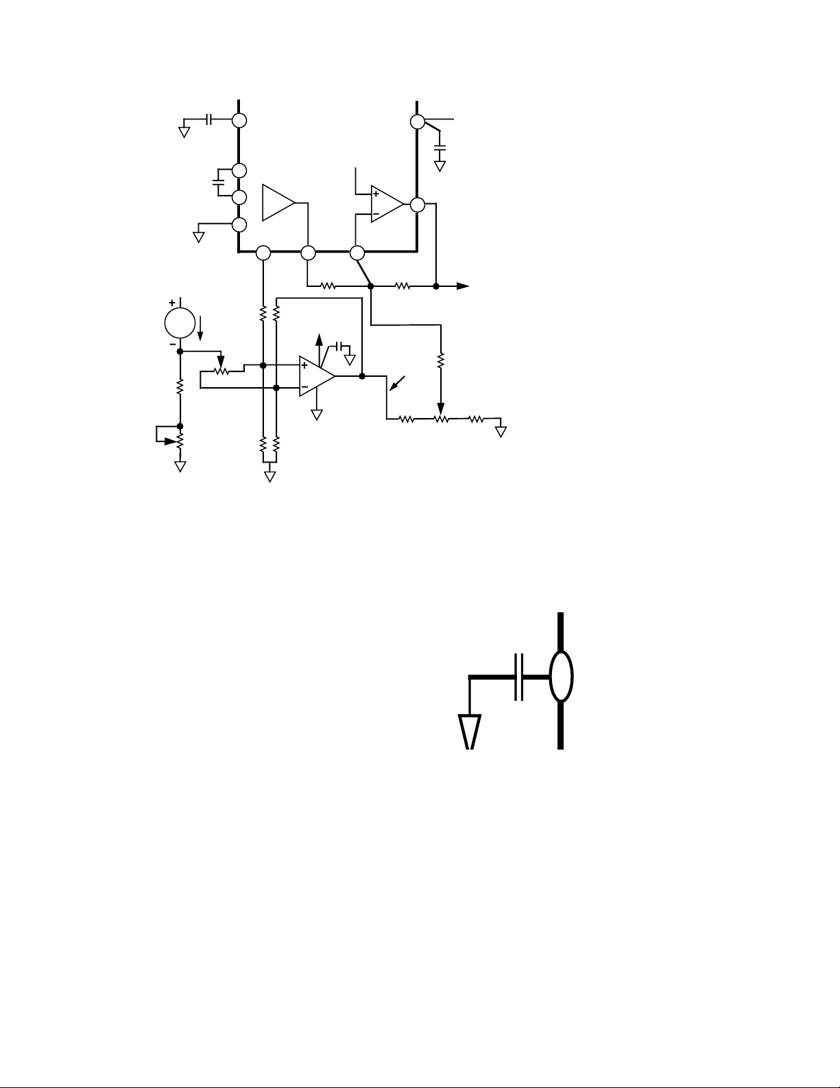
Figure 2. ADXL50 0 g Drift Compensation Circuit
CALIBRATION PROCEDURE:
AT T
OR LOWER TEMP CAL. POINT:
MIN
1. SET RB ALL THE WAY TO ONE SIDE.
2. ADJUST RA FOR +3.4V AT
TEST POINT “A.”
3. SET RC FOR +2.5V V
(AT PIN 9 OF ADXL50).
TO TEST THE CIRCUIT:
4. TEMORARILY CONNECT A 1.5kΩ
RESISTOR BETWEEN THE WIPER
OF RB AND COMMON.
5. ADJUST RB FOR +2.5V AT V
6. REMOVE THE 1.5kΩ RESISTOR.
V
SHOULD NOT CHANGE.
OUT
AT T
OR UPPER TEMP CAL. POINT:
MAX
7. GO TO T
8. READJUST RB FOR +2.5V @ V
9. CALIBRATION COMPLETE.
MAX
OUT
.
OUT
OR HIGH TEMP CAL . POINT .
OUT.
E1913–12–5/94
A Hardware Approach
The circuit of Figure 2 provides a linear temperature compensation for the ADXL50. Figure 3 shows the 0 g drift
over temperature for a typical ADXL50 with and without
this circuit. As shown by Figure 3, the linear portion of the
drift curve has been subtracted out. In effect, the curve
has been rotated counter clockwise until it is horizontal,
leaving just the bow of the curve: that portion which is not
linear.
As shown in Figure 3, over a +25 °C to +70°C range, a 10 ×
reduction in drift is achieved. The circuit of Figure 2 is essentially a temperature sensor coupled to a forcedbalance bridge. The AD590 provides a 1 µ A/°K current
output whose voltage scale factor is set by resistor RA.
The bridge circuit subtracts out the nominal 298 mV output of the AD590 at +25 °C and leaves only the change in
temperature, which is what is needed.
Resistors R5 and R6 form a resistor divider (one half of the
bridge) which divides down the +3.4 V reference output of
the ADXL50 to 0.3 V which appears at the noninverting
input of the AD820 op amp. Resistors R7 and R8 form the
other half of the bridge, and because they have the same
ratio as R5 and R6 the op amp will have a +3.4 V output at
room temperature. Therefore, the op amp is across the
output of the bridge and any imbalance will cause its output to change enough to maintain the summing junction
at 0.3 V, which keeps the bridge in balance.
C2
4
ADXL50
0.022µF
Figure 3. ADXL50 0 g Drift With & Without the Compensation Circuit of Figure 2
The output from the AD590 connects to the wiper of trim
potentiometer R B. Since R B is across the input terminals
of the op amp, the circuit can provide a variable output
with temperature in either the positive or negative direction. The op amp output is divided down by resistors R9
and R10 which limit the range of trim potentiometer RC
and increase its resolution. Resistors R1 and R3 set the
ADXL50 accelerometer's gain at ten (190 mV/g) which is
appropriate at low g levels, while R2 and R3 set the gain of
the compensation circuit.
PRINTED IN U.S.A.
–2–
 Loading...