

Page 1
AN-374
1.5
g
150m
g
15m
g
1.5m
g
150µ
g
3dB BANDWIDTH – Hz
NOISE LEVEL – Peak to Peak
NOISE LEVEL – rms
10
g
1m
g
10m
g
100m
g
1
g
10 100 1k
ADXL05
ADXL50
a
ONE TECHNOLOGY WAY • P.O. BOX 9106
Using Accelerometers in Low g Applications
INTRODUCTION
Accelerometers can be used in a wide variety of low
applications such as tilt and orientation, vibration analysis, motion detection, etc. This application note explains
how to best apply the ADXL50 (50
accelerometers when measuring signals at the low end
of their respective full-scale ranges. Although each
accelerometer is specified according to its full scale
(clipping)
i.e., its minimum discernible input level, is extremely important when measuring low
The limiting resolution is predominantly set by the measurement noise “floor” which includes the ambient
background noise and the noise of the accelerometer itself. The level of the noise floor varies directly with the
bandwidth of the measurement. As the measurement
bandwidth is reduced, the noise floor drops, improving
the signal-to-noise ratio of the measurement and its
limiting resolution.
g
level, the limiting resolution of the device,
g
) and ADXL05 (5 g)
g
accelerations.
•
NORWOOD, MASSACHUSETTS 02062-9106
by Charles Kitchin
g
APPLICATION NOTE
617/329-4700
•
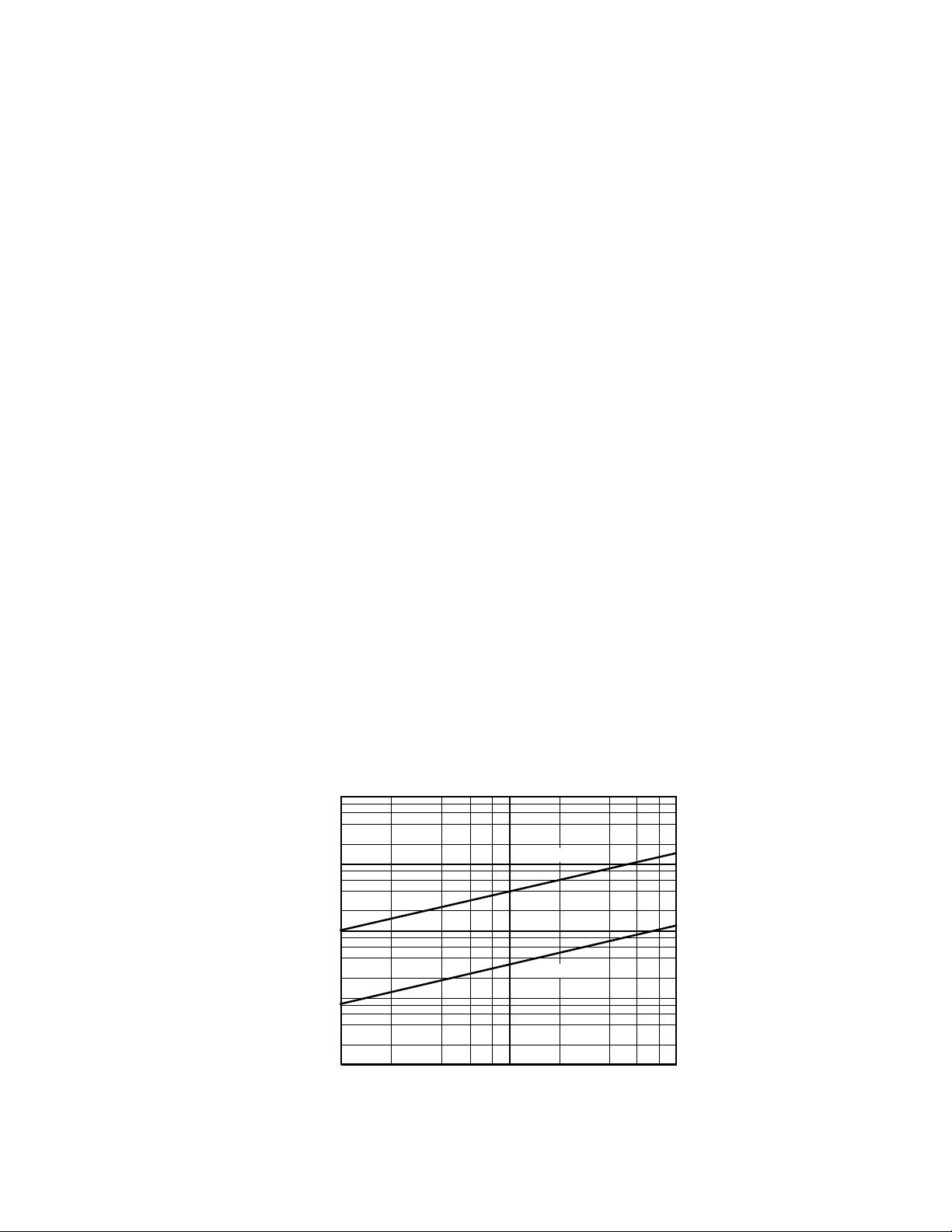
DEVICE BANDWIDTH VS. MEASUREMENT RESOLUTION
The output noise of the ADXL50 and ADXL05 scales
with the square root of the measurement bandwidth.
The maximum amplitude of the noise, its peak-to-peak
value, approximately defines the worst-case resolution
of a measurement. The peak-to-peak noise is approximately equal to 6.6 times its rms value (for an average
uncertainty of 0.1%).
The bandwidth of the accelerometer can be easily reduced by adding low-pass or bandpass filtering. Figure
1 shows the noise vs. bandwidth characteristics of the
ADXL50 and ADXL05 devices.
As shown by the figure, device noise drops dramatically
as the operating bandwidth is reduced. For
example, when operated in a 1 kHz bandwidth, the
ADXL05 typically has a peak-to-peak noise level of
130 m
g
. With ±5 g applied accelerations, this 130 m
resolution limit is normally quite satisfactory; but for
g
Figure 1. Noise Level vs. 3 dB Bandwidth
Page 2
smaller acceleration levels the noise is now a much
greater percentage of the signal. As shown by Figure 1,
when the device bandwidth is rolled off to 100 Hz, the
peak-to-peak noise level is reduced to approximately
40 m
g
, and at 10 Hz it is down to 10 mg.
0
g
offset trimming, and output scaling. Two tables are included with the figure which provide practical component
values for various full-scale
g
levels and approximate circuit bandwidths. For bandwidths other than those listed,
use the formula:
Alternatively, the signal-to-noise ratio may be improved
considerably by using a microprocessor to perform
multiple measurements and then compute the average
signal level. When using this technique, the signal level
will be increased directly with the number of measurements while the noise will only increase by their square
root. For example, with 100 measurements, the signal-tonoise ratio will be increased by a factor of 10 (20 dB).
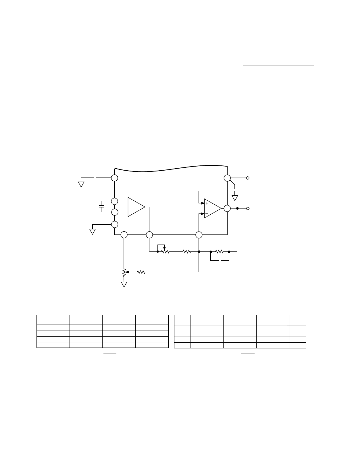
Low-Pass Filtering
The bandwidth of either accelerometer can be reduced by
providing post filtering. Figure 2 shows how the buffer
amplifier can be connected to provide 1-pole post filtering,
C2
4
0.022µF
0.022µF
C1
COM
C1
2
3
5
+3.4V
REF
ADXL50 OR ADXL05
PRE-AMP
6
8
V
PR
Capacitor C4 (Farads) =
2 π×R3(Ω)×3dB BW (Hz)
1
or simply scale the value of capacitor C4 accordingly, i.e.,
for an application with a 50 Hz bandwidth, the value of C4
will need to be twice as large as its 100 Hz value. If further
noise reduction is needed while maintaining the maximum possible bandwidth, then a 2- or 3-pole post filter is
recommended. These provide a much steeper roll-off of
noise above the pole frequency. Figure 3 shows a circuit
that uses the buffer amplifier to provide 2-pole post filtering. Component values for the 2-pole filter were selected
to operate the buffer at unity gain.
0.1µF
+5V
V
OUT
R1a
R1b
1.8V
10
BUFFER
–
V
IN
1
AMP
9
R3
OPTIONAL SCALE
0
g
LEVEL
TRIM
FACTOR TRIM*
R2
50kΩ
*TO OMIT THE OPTIONAL SCALE FACTOR
TRIM , REPLACE R1a AND R1b WITH A
C4
FIXED VALUE 1% METAL FILM RESISTOR.
SEE VALUES SPECIFIED IN TABLES BELOW.
ADXL50 COMPONENT VALUES FOR VARIOUS
FULL-SCALE RANGES AND BANDWIDTHS
FULL
SCALE
±10
±20
±10
±20
mV
3dB
R1a
per
g
BW (Hz)
200
g
g
g
g
100
200
100
100
100
10
10
3dB BW =
R1b
kΩ
kΩ
21.5
5
23.7
5
21.5
5
23.7
5
1
2π R3 C4
R3
kΩ
249
137
249
137
R2
kΩ
100
100
100
100
C4
µF
0.0068
0.01
0.068
0.01
ADXL05 COMPONENT VALUES FOR VARIOUS
FULL-SCALE RANGES AND BANDWIDTHS
FULL
SCALE
±1
g
±2
g
±4
g
±5
g
mV
per
2000
1000
500
400
3dB
g
BW (Hz)
10
100
200
300
3dB BW =
R1a
kΩ
10
10
10
10
R1b
kΩ
24.9
35.7
35.7
45.3
1
2π R3 C4
301
200
100
100
R3
R2
kΩ
100
100
100
100
C4
µF
0.056
0.0082
0.0082
0.0056
kΩ
Figure 2. Using the Buffer Amplifier to Provide 1-Pole Post Filtering Plus Scale Factor and 0 g Level Trimming
–2–
Page 3
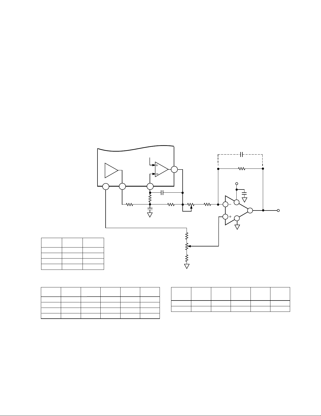
Capacitors C3 and C4 were chosen to provide 3 dB bandwidths of 10 Hz, 30 Hz, 100 Hz, and 300 Hz.
In this configuration, the nominal buffer amplifier output will be +1.8 V ± the scale factor of the accelerometer,
either 19 mV/
g
for the ADXL50 or 200 mV/g for the
ADXL05. An AD820 external op amp allows
noninteractive adjustment of 0
g
offset and scale factor.
The external op amp offsets and scales the output to
provide a +2.5 V ± 2 V output over a wide range of fullscale
g
levels.
Additional Noise Reduction Techniques
In addition to reducing circuit noise, any electromagnetic interference (EMI) needs to be considered.
Shielded wire should be used for connecting the accelerometer to any equipment or circuitry that is more than
a few inches away. A common problem is that of 60 Hz
PRE-AMP
ADXL50
1.8V
OR
ADXL05
V
IN
R5
42.2kΩ
10
–
2-POLE FILTER
COMPONENT VALUES
3dB
BW (Hz)
300
100
30
10
C3µF
0.027
0.082
0.27
0.82
C4µF
0.0033
0.01
0.033
0.1
6
V
REF
8
V
PR
R1
82.5kΩ
BUFFER
AMP
9
C4
R3
C3
82.5kΩ
2-POLE FILTER
40.2kΩ
20kΩ
71.5kΩ
pickup from ac line voltage. This can be minimized by
physically moving the device away from power leads, or
if that is not practical, using proper shielding and
grounding techniques. In most cases, it is advisable to
ground the cable’s shield at only one end and connect a
separate common lead between the circuits; this will
help to prevent ground loops. Also, if the accelerometer
is inside or near a metal enclosure, this should be
grounded as well.
Another area to consider is mechanical resonance of the
overall measurement system. The use of a highly flexible shielded wire will greatly help to prevent secondary
resonance effects of wire vibrating at its natural frequency. A shielded cable with a silicone jacket and silicone insulation such as that produced by Cooner Wire
Company of Chatsworth, California, is recommended.
OPTIONAL CAPACITOR
FOR 3-POLE FILTERING
2
AD820
3
R5
+5V
7
4
0.01µF
6
OFFSET AND
SCALING
AMPLIFIER
OUTPUT
V
OUT
+3.4V
R6
R7
R4a
SCALE
FACTOR
TRIM
0
g
LEVEL
TRIM
R4b
FULL
SCALE
±1
g
±2
g
±4
g
±5
g
ADXL05 OFFSET AND SCALING
AMPLIFIER COMPONENT VALUES
mV per
2000
1000
500
400
g
GAIN
10.00
4.98
2.50
2.00
R4a
kΩ
10
10
10
10
Figure 3. Two-Pole Filtering Circuit with Gain and 0 g Offset Adjustment
R4b
kΩ
24.9
35.7
35.7
45.3
301
200
100
100
ADXL50 OFFSET AND SCALING
AMPLIFIER COMPONENT VALUES
R5
kΩ
SCALE
FACTOR IN
mV/
g
200
100
MAX
INPUT
±10
±20
GAIN
g
10.53
g
5.26
R4a
kΩ
5
5
R4b
kΩ
21.5
23.7
R5
kΩ
249
137
–3–
Page 4

OFFSET DRIFT CONSIDERATIONS
When using an accelerometer with a dc (gravity sensing)
response, the 0
ture drift. When the accelerometer must measure low
g
offset level will exhibit some tempera-
g
levels over wide temperature ranges, the 0 g drift can become large in proportion to the signal amplitude. If a dc
response is truly needed, there are a number of design
options available. One very straightforward approach is to
use a low cost crystal oven to maintain the accelerometer
at a constant temperature. These ovens are particularly
useful in high accuracy tilt applications. After the circuit
has been built and is operating correctly, the crystal oven
can be mounted over the accelerometer and powered off
the same +5 V power supply. Figure 4 shows the basic circuit.
The ovens may be purchased from Isotemp Research, Inc.,
P.O. Box 3389, Charlottesville, VA 22903, phone 804-295-
3101. For more details on crystal oven compensation, refer to application note AN-385.
Other methods for 0
g
drift compensation include using a
low cost temperature sensor such as the AD590 to supply
a microprocessor with the device temperature. If the drift
curve of the accelerometer is stored in the µP, then a software program can be used to subtract out the drift. This
method works well, removing both the linear and nonlinear components of the drift. But due to device-to-device
variation, it requires that the drift curve of each individual
accelerometer be known (or measured). Alternatively,
various drift compensation circuits can be used to subtract
out the
linear portion of the accelerometer’s drift by using
a temperature sensor and op amp to supply a small compensation current. This hardware approach does not use a
µP but does require calibrating the compensation circuitry
for each device. For more details on software and hardware drift compensation, refer to application note AN-380.
ADXL50
OR
ADXL05
PRE-AMP
V
PR
6
+3.4V
REF
FS MEASUREMENT
V
PR
RANGE*
±10
g
±2
g
8
R1
SENSITIVITY
1.8V
10
OUTPUT
100mV/
500mV/
V
IN
g
g
BUFFER
AMP
–
1
9
R3
C
F
BUFFER
GAIN
5.26
2.50
C3
0.1µF
V
OUT
0g TOLERANCE.
PR
+5V
V
OUT
R1 R3
26.1k
40.2k
137k
100k
ISOTEMP
1µF
1.5µF
0.022 µF
0.022µF
ADXL50
ADXL05
C2
4
C1
2
3
C1
5
COM
0g OUTPUT – +2.5V
3dB Bw – 1Hz
DEVICE
*FS RANGE NUMBERS ARE CONSERVATIVE TO ALLOW FOR V
Figure 4. Low g DC Coupled (Tilt) Circuit Using Crystal Oven Compensation
M050570
+5V
+VDC
1
3
0VDC
C
F
2
NC
–4–
Page 5

AC Coupling
If a dc (gravity) response is not required—for example in
motion sensing or vibration measurement applications—ac coupling can be used between the preamplifier output and the buffer input as shown in Figure 5.
Because ac coupling removes the dc component of the
output, the preamp output signal may be amplified considerably without increasing the 0
g
level drift. If capacitor C5 is added to the ac coupling circuit, forming a
1-pole low-pass filter, then a bandpass function is provided that will attenuate any signals other than those
within the pass band. A typical ac coupled frequency response is shown in Figure 6.
The low frequency roll-off, F
, due to the ac coupling net-
L
work is:
F
L
1
=
R1C
2 π
4
In this case, the high frequency roll-off, FH, is determined
by the 1-pole post filter R3, C5.
If ac coupling is used, the self-test feature must be monitored at V
, rather than at the buffer output (since the
PR
self test output is a dc voltage).
20
10
LOW FREQUENCY ROLL-OFF ( FL )
0
–10
–20
NORMALIZED OUTPUT LEVEL – dB
–30
0.1 1 10 100 1k
HIGH FREQUENCY ROLL-OFF ( FH )
FREQUENCY – Hz
Figure 6. Typical Output vs. Frequency Curve when AC
Coupling V
to the Buffer
PR
Note that capacitor C4 should be a nonpolarized, low
leakage type. If a polarized capacitor is used, tantalum
types are preferred, rather than electrolytic. With polarized capacitors, V
should be measured on each device
PR
and the positive terminal of the capacitor connected toward either V
or VIN—whichever is more positive.
PR
COMPONENT
VALUES ARE
APPROXIMATE.
FOR MAXIMUM
ACCURACY,
SCALE FACTOR
TRIMMING SHOULD BE
EMPLOYED.
IN
IN
g
g
DESIRED
LOW
FREQUENCY
LIMIT, F
L
30
10
3
1
0.1
DESIRED
LOW
FREQUENCY
LIMIT, F
L
30
30
3
1
0.1
SCALE
FACTOR
mV/
200
100
200
100
200
SCALE
FACTOR
mV/
1000
200
1000
200
200
R1
VALUE
IN kΩ
24
24
24
24
24
R1
VALUE
IN kΩ
49.9
249
49.9
249
249
PRE-AMP
ADXL50
CLOSEST
C4
VALUE
0.22µF
0.68µF
2.2µF
6.8µF
68µF
ADXL05
CLOSEST
C4
VALUE
0.10µF
0.022µF
1.0µF
0.68µF
6.8µF
ADXL50 OR ADXL05
V
PR
8
V
PR
DESIRED
FREQUENCY
LIMIT, F
DESIRED
FREQUENCY
LIMIT, F
HIGH
300
300
100
100
10
HIGH
300
300
100
100
10
C4
R1
IN kΩ
H
249
127
249
127
249
IN kΩ
H
R3
R3
249
249
249
249
249
1.8V
10
–
V
IN
R2
CLOSEST
C5
VALUE
0.002µF
0.0039µF
0.0068µF
0.01µF
0.068µF
CLOSEST
C5
VALUE
0.002µF
0.002µF
0.0068µF
0.0068µF
0.068µF
BUFFER
AMP
R3
C5
V
9
VALUE
OF R2
FOR +2.5V
0
g
LEVEL
640kΩ
326kΩ
640kΩ
326kΩ
640kΩ
VALUE
OF R2
FOR +2.5V
0
g
LEVEL
640kΩ
640kΩ
640kΩ
640kΩ
640kΩ
OUT
Figure 5. AC Coupling the VPR Output to the Buffer Input
–5–
Page 6

GAIN SELECTION ISSUES
0
g
(a)
0
g
(b)
–1
g
(c)
+1
g
(d)
INDICATED POLARITY IS THAT
OCCURING AT V
PR
The uncommitted amplifier incorporated into the ADXL50
and ADXL05 devices allows the user to readily set the
scale factor to the desired voltage output per
g
of applied
acceleration. However, some caution is advised in not setting the scale factor, too high as the output buffer could
run out of “headroom,” i.e., the buffer’s output can go as
low as 0.25 volts and as high as 4.75 volts. This means the
buffer’s maximum output swing is +2.5 V ± 2.25 V. If the
gain is too high, the buffer can clip on periodic transient
accelerations; or it can clip due to the fact that the 0
g
off-
set drift is also amplified along with the signal.
Therefore, use only enough gain in the buffer as is neces-
sary to override any transmission losses between the accelerometer and any following circuitry (i.e., to keep the
system’s signal to noise ratio high).
Using the Earth’s Gravity to Calibrate the Accelerometer
Both the 0g offset and scale factor of the ADXL50 and
ADXL05 devices may be roughly calibrated by using the
1
g
(average) acceleration of the Earth’s gravity. Figure 7
shows how gravity and package orientation affect the output polarity. Note that the output polarity is that which appears at V
; the output at V
PR
will have the opposite sign
OUT
(due to the buffer amplifier’s inverting configuration).
With its axis of sensitivity in the vertical plane, the accelerometer should register a 1
g
acceleration, either positive
or negative, depending on orientation. With the axis of
sensitivity in the horizontal plane, no acceleration (0
g
)
should be indicated.
Calibrate the accelerometer by placing it on its side with
its axis of sensitivity oriented as shown in “a.” The 0
g
offset potentiometer, RT, (as shown in Figure 2) is then
roughly adjusted for midscale: +2.5 V at the buffer output.
Figure 7. Using the Earth’s Gravity to Calibrate the
ADXL50 and ADXL05 Accelerometers
If the optional scale factor trimmer, R1a, is to be used, it
should be adjusted next. The package axis should be oriented as in “c” (pointing down) and the output reading
noted. The package axis should then be rotated 180° to
position “d” and R1a adjusted so that the output voltage
indicates a change of 2
the circuit scale factor at the buffer output is 200 mV per
g
s in acceleration. For example, if
g
then the scale factor trim should be adjusted so that an
output change of 400 mV is indicated.
Adjusting the circuit’s scale factor will have some effect
on its 0
g
level, so this should be readjusted, as before, but
this time checked in both positions “a” and “b.” If there is
a difference in the 0
g
reading, a compromise should be
selected so that the reading in each direction is equal distant from +2.5 V. Scale factor and 0
g
offset adjustments
should be repeated until both are correct.
APPLICATIONS ASSISTANCE
For applications assistance contact Charles Kitchin,
Accelerometer Applications, Analog Devices Semiconductor, 831 Woburn St., Wilmington, MA 01887. Phone:
617-937-1665.
E2007–9–3/95
,
PRINTED IN U.S.A.
–6–
 Loading...