

Page 1
AN-273
a
APPLICATION NOTE
One Technology Way • P.O. Box 9106 • Norwood, MA 02062-9106 • 781/329-4700 • World Wide Web Site: http://www.analog.com
Use of the AD590 Temperature Transducer
in a Remote Sensing Application
by Paul Klonowski
INTRODUCTION
The AD590 is a two-terminal integrated circuit temperature transducer that produces an output proportional to
absolute temperature. For supply voltages between +4 V
and +30 V the device acts as a high impedance, constant
current source supplying 1 µA/K. Laser trimming of the
chip’s thin-film resistors is used to calibrate the device
to an output of 298.2 µA at 298.2K (+25°C).
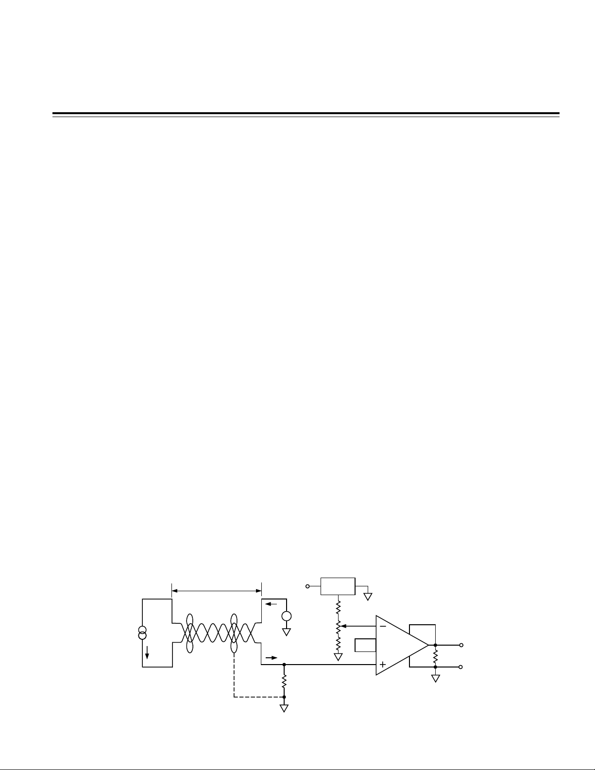
A typical application for the AD590 is a remote temperature-to-current transducer. Figure 1 shows a thermom-
eter circuit that measures temperature from –55°C to
+100°C and whose output voltage is 100 mV/°C. Since
the AD590 measures absolute temperature (its nominal
output is 1 µA/K), the output must be offset by 273.2 µA
in order to read out in degrees Celsius. The output cur-
rent of the AD590 flows through a 1 kΩ resistance, devel-
oping a voltage of 1 mV/K. The output of the AD580 2.5 V
reference is divided down by resistors to provide a
273.2 mV offset, which is subtracted from the voltage
across the 1 kΩ resistor by an AD524 instrumentation
amplifier. The amplifier provides a gain of 100, so that
the output range corresponding to –55°C to +100°C is
–5.5 V to +10 V (100 mV/°C). An operational amplifier can
substitute for the instrumentation amplifier, although
care must be taken when designing with the
op amp since the gain at the two input terminals will be
different.
THE PROBLEM
A question often asked of Analog Devices Applications
Engineers by customers using the AD590 in a remote
temperature-to-current application is, “How long can I
make the cable and how can I eliminate any noise that
the cable picks up?” Experiments were performed in an
effort to provide some guidelines for answering this
question using the circuit of Figure 1 with a 1000'
shielded, though initially ungrounded, twisted pair cable
(Belden 9461, style 2092). In order to duplicate actual
conditions the experiments were performed in an industrial environment.
TYPES OF NOISE
There are three basic types of noise inherent in a
data-acquisition system. The first type is
noise
: noise received with the original signal and indis-
tinguishable from it. The second type is
transmitted
intrinsic noise:
noise generated within the devices used in a circuit, e.g.,
resistors, op amps, etc. Included in this category are
Johnson, shot and popcorn noise. The third type is
induced noise
: noise picked up from the outside world
and coupled into the circuit. This application note discusses methods of reducing induced noise, which is the
only form of noise that can be influenced by choices of
wiring and shielding.
AD590
I
T
I
T
I
T
+15V
+
7V
–
0.1% LOW
TCR RESISTOR
1mV/K
<
Figure 1. Thermometer Circuit
1kV
AD580
909kV
200V
1kV
G = 100
RG
AD524
2
INSTRUMENTATION AMP
GAIN = 100, 100mV/8C
2kV
E
O
Page 2
AN-273
NOISE FACTORS
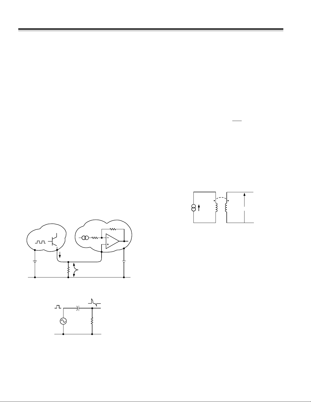
Three elements are involved in any noise problem. The
first is the source of the noise. Possible noise sources
include AM radio signals, logic signals, magnetic fields
and power line transients. The second element is the
coupling medium. That is, how is the noise source entering the circuit? Possible coupling mediums include a
common circuit impedance (Figure 2), stray capacitance
(Figure 3) and mutual inductance (Figure 4). A brief description of each follows.
Common impedance noise is developed by an impedance common to several circuits. This might occur, as
shown in Figure 2, when a pulse output source and an
op amp’s reference terminal are both connected to a
“ground” point having tangible impedance to the
power supply terminal. The noisy return current of Circuit 1 develops a voltage, V
, across the common im-
NOISE
pedance Z which will appear as a noise signal to Circuit
2. Possible solutions to this problem include proper circuits for distributing power and the use of isolation
transformers and optical isolators.
Capacitively-coupled noise is produced by stray capacitance which couples the voltage changing noise source
into high impedance circuits, as shown in Figure 3. The
nature of the impedance Z determines the shape of the
response. Methods of reducing capacitively-coupled
noise include reducing the noise source, properly implementing shields and reducing the stray capacitance.
Magnetically coupled noise is produced by mutual inductance and can occur, for example, in an incorrectly
shielded cable as shown in Figure 7. Figure 4 is a simple,
model of this incorrectly shielded cable, where L
sents the inductance of the shield, L
represents the in-
C
repre-
S
ductance of one of the center conductors, and L
represents the mutual inductance between the two. The
noise current l(t) flows through L
and establishes a
S
magnetic flux; this time-varying flux also surrounds L
and produces a voltage V
rate of change of the current I(t) flowing through L
proportional to the time
NOISE(t)
. This
S
voltage can be expressed as
dI(t)
V
NOISE(t)
=
LM
dt
The third element involved in any noise problem is the
receiver, or the circuit susceptible to the noise. It is important to understand the role of each of the three elements (the noise source, the coupling medium, and the
receiver) in order to solve the noise problem*. In this
experiment it was determined that the noise sources
were 60 Hz pickup and AM radio signals, the coupling
medium was stray capacitance and the receiver was the
AD524.
L
M
L
I
(t)
L
S
V
C
NOISE(t)
M
C
CIRCUIT 2
= I
V
NOISE
NOISE
POWER SUPPLY COMMON
V
S1
CIRCUIT 1
+
I
Z
COMMON
IMPEDANCE
NOISE
Figure 2. Common Impedance Noise
C
S
V
NOISE
SOURCE
Z
Figure 3. Stray Capacitance Noise
Z
V
NOISE
Figure 4. Mutual Inductance Noise
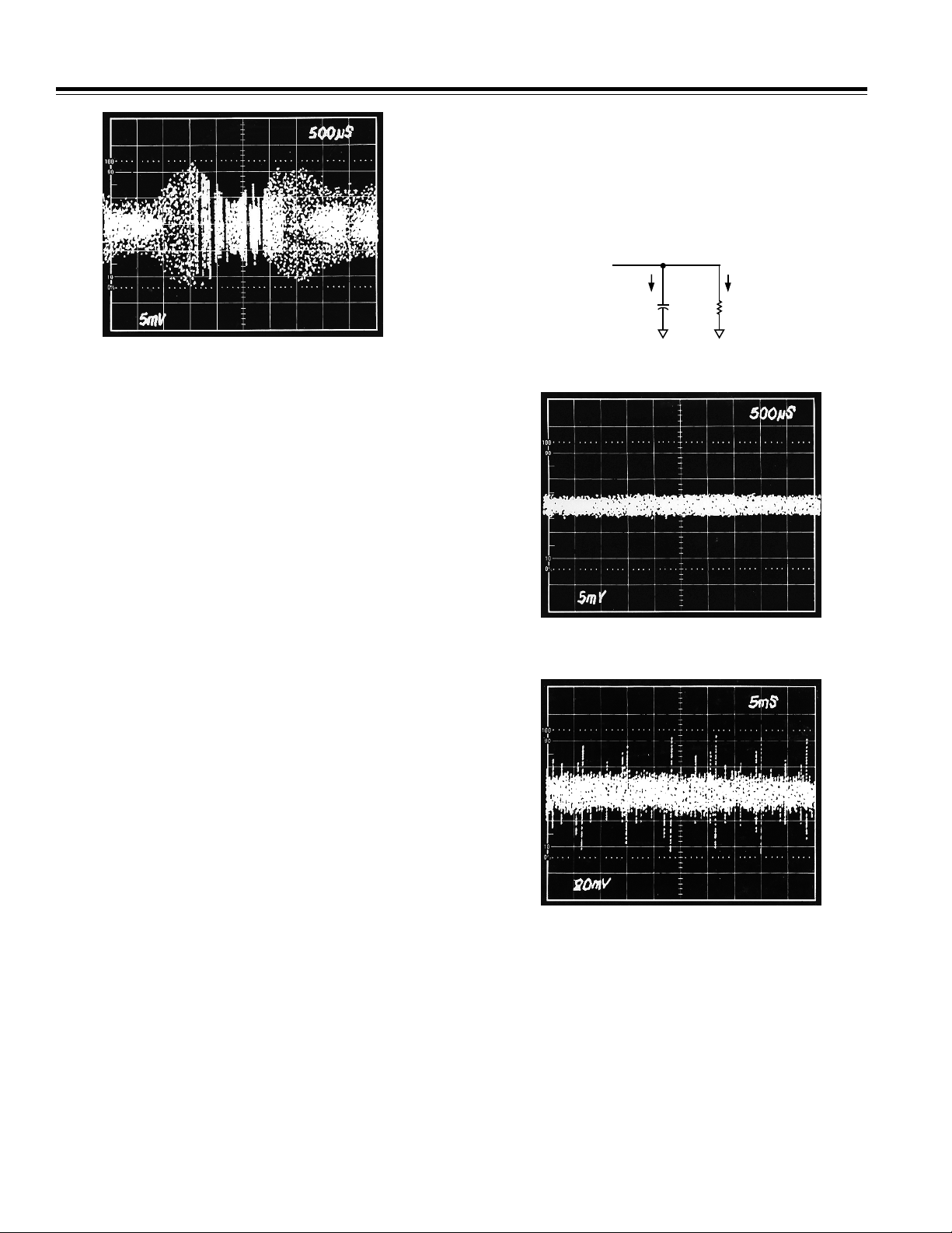
INITIAL NOISE EFFECT
The photograph in Figure 5 shows the output of the circuit in Figure 1 with the shield ungrounded and with the
+
V
S2
remote AD590 at 30°C. Ideally, the output should be a
3 V (100 mV/°C) dc signal. However, a 60 Hz signal result-
ing from an electric field has been capacitively coupled
into the circuit via the stray capacitance of the cable and
then amplified by a gain of 100. Note, however, that the
60 Hz signal is offset by a dc signal; when the output
voltage of the AD524 was measured with a dc voltmeter
the value read was 3.0 V. This is because the voltmeter
read the value of the dc signal due to the AD590 along
with the average value of the 60 Hz sine wave noise signal. The average value of a sine wave is zero. In essence,
notwithstanding the interfering signal the average value
was correct. The accuracy of all the measurements were
verified through the use of an RTD measurement system; the AD590 under test was physically attached to
the RTD.
*An excellent article dealing with this subject is “Understanding Inter-
ference-Type Noise” by Alan Rich, found in Section 20 of the Analog
Devices Databook.
–2–
Page 3

AN-273
Figure 5. EO (Figure 1) with Shield Ungrounded
SHIELDING
One effective way to eliminate electrostatic noise is to
use shielding. A charge resulting from an external potential cannot exist on the interior of a closed conducting surface. A shield is, in effect, a closed conducting
surface that surrounds the twisted pair of wires within
the cable.
In order for a shield to be effective it should be connected to the reference potential of any circuitry contained within the shield. If the signal is connected to
earth ground, then the shield should be connected to
earth ground (see Figure 6). No voltage should exist between the reference potential and the shield conductor.
V
SIG
REFERENCE POTENTIAL
LOAD
Figure 6. Correctly Shielded Cable
Figure 8. EO with Shielded Grounded
Although the 60 Hz signal noise has been eliminated,
voltage spikes are still visible in Figure 8. Figure 9, which
is another view of the AD524 output with the scope ac
coupled and the scale magnitude increased, shows the
high frequency noise still being picked up by the cable.
A look at Figure 10, which is a view of the signal being
fed into the noninverting terminal of the AD524, shows
that the noise being picked up is actually an AM radio
signal.
RF NOISE
RF noise is a combination of an electric field and a magnetic field, or an electromagnetic field. This electromagnetic field extends into and beyond the space between
conductors. That is, the electromagnetic field and hence
the RF energy is “steered” by the conductors.
V
SIG
"GROUND 1"
V
COMMON
I
"GROUND 2"
LOAD
Figure 7. Incorrectly Shielded Cable
Only one end of the shield should be tied to “ground.”
Tying both ends of the shield to “ground” will produce a
shield current equal to the difference in the potential of
the two “grounds” divided by the series resistance of
the shield (see Figure 7). As previously discussed, the
mutual inductance between the shield and conductors
will couple this noise current into the conductors in the
form of a series voltage, V
NOISE
.
–3–
Figure 9. RF Noise at E
O
Page 4
AN-273
I
NOISE
1kV
I
DC
0.33mF
In this instance the radio carrier frequency was 550 kHz.
It is important not to ignore RF noise, even if the bandwidth of the external circuitry is smaller than the bandwidth of the RF noise. A large RF component will
overload the inputs of the external circuitry and be detected, causing an apparent dc shift in the component’s
output signal.
Figure 10. RF Noise at AD524 +Input
RF energy both enters and is reflected in a system wherever there is an impedance mismatch or discontinuity in
the system. This includes discontinuities at the end of
the signal run; at the AD590 end and the AD524 end of
the cable. In order to eliminate these discontinuities it
would be necessary to RF shield the entire circuit system, perhaps using conduit and metal boxes. In most
cases however, this is rather impractical.
What is usually sufficient for most systems is to provide
RF filtering using passive components at the critical
point of interest. It is important to note that this filter
may not eliminate the RF energy but it may just reflect
the energy and redistribute the problem. A circuit topology which ensures that none of the external circuitry is
affected by the RF noise is discussed later.
BYPASS CAPACITORS
A bypass capacitor can be used to divert some of the
high frequency noise current to ground. Figure 11 is a
simple schematic that shows the effect of the bypass
capacitor. Recalling that the reactance of a capacitor
X
= 1/2 π fC and assuming that we have the minimum
C
radio carrier frequency of 550 kHz, using a 0.33 µF ca-
pacitor the impedance seen by the noise current is:
Figure 11. Bypass Capacitors Reduce RF Noise Effect
Figure 12. AD524 +Input with Bypass Capacitor
X
=1/2 π (550 × 103)(0.33 × 10⁻⁶) = 0.88 Ω
C
Of course the direct current supplied by the AD590
will be unaffected by the bypass cap and will continue to
flow into the 1 kΩ resistor. Only the high frequency
noise current will be affected. Figure 12, which is a view
of the signal at the AD524 noninverting terminal, shows
the result of tying a 0.33 µF capacitor across the 1 kΩ
"load” resistor with the shield still grounded. Figure 13
is a look at the output signal of the AD524 with the
0.33 µF capacitor. Compare Figures 10 and 12, and Fig-
ures 9 and 13. The bypass capacitor reduces the noise
magnitude by a factor greater than 5.
Figure 13. EO with Bypass Capacitor
–4–
Page 5
SERIES RESISTORS
Although an improvement, Figure 13 shows that noise is
still entering the circuit. Another method of reducing the
amount of noise seen at the noninverting terminal of the
op amp is to limit the noise currents through the cable
by adding 1 kΩ resistors in series with the AD590.
This in effect forms a noise-voltage divider between the
load impedance (the 1 kΩ resistor and the 0.33 µF ca-
pacitor) and the series resistors. Figure 14 shows the
output of the AD524 with this final circuit configuration.
The 10 mV p-p amplitude of the output noise is actually
100
× the amplitude of the noise seen at the input of the
AD524, which is 100 µV p-p. Note also that the high fre-
quency spikes in Figure 13 have been eliminated in Figure 14. Figure 15 is the schematic of the final circuit
which has reduced the noise by a factor of 2000 over the
circuit in Figure 1.
AN-273
Figure 14. EO with Bypass Capacitor and Series Resistors
I
T
AD590
<
1kV
I
T
I
T
1kV
0.33mF
+15V
AD580
909kV
+
7V
–
200V
1kV
1kV
G = 100
RG
2kV
E
O
AD524
2
Figure 15.
–5–
Page 6

AN-273
CONCLUSION
In order to eliminate the effects of RF noise, the circuit of
Figure 16 is recommended.
In Figure 16, the resistors and capacitors are placed at
both ends of the cable. This ensures that the RF noise
remains within the cable and does not affect the external
circuitry. Further note that these resistors can be arbitrarily large as long as the voltage potential is large
enough to supply the current (V = IR). The use of a by-
R
C
R
AD590
<
R
R
0.33mF
pass capacitor across the AD590 with the series resistors
will filter RF signals. Theoretically the RF signal could
be rectified by the AD590 and offset the accuracy of the
device.
Using the techniques outlined above, noise and interference can be effectively eliminated through the use of
shielded twisted pair cable and resistors and capacitors.
Thus it is possible to drive the AD590 over 1000 feet of
cable without a loss of accuracy.
E920a–0–7/98
+15V
C
AD580
909kV
+
7V
–
200V
1kV
1kV
G = 100
RG
2kV
E
O
AD524
2
Figure 16.
PRINTED IN U.S.A.
–6–
 Loading...