

ANALOG DEVICES ADXL103 Service Manual
Precision ±1.7 g, ±5 g, ±18 g Single-/
Data Sheet
FEATURES
High performance, single-/dual-axis accelerometer on
a single IC chip
5 mm × 5 mm × 2 mm LCC package
1 mg resolution at 60 Hz
Low power: 700 μA at V
High zero g bias stability
High sensitivity accuracy
−40°C to +125°C temperature range
X and Y axes aligned to within 0.1° (typical)
Bandwidth adjustment with a single capacitor
Single-supply operation
3500 g shock survival
RoHS compliant
Compatible with Sn/Pb- and Pb-free solder processes
Qualified for automotive applications
APPLICATIONS
Vehicle dynamic controls
Electronic chassis controls
Platform stabilization/leveling
Navigation
Alarms and motion detectors
High accuracy, 2-axis tilt sensing
Vibration monitoring and compensation
Abuse event detection
= 5 V (typical)
S
Dual-Axis iMEMS
®
Accelerometer
ADXL103/ADXL203
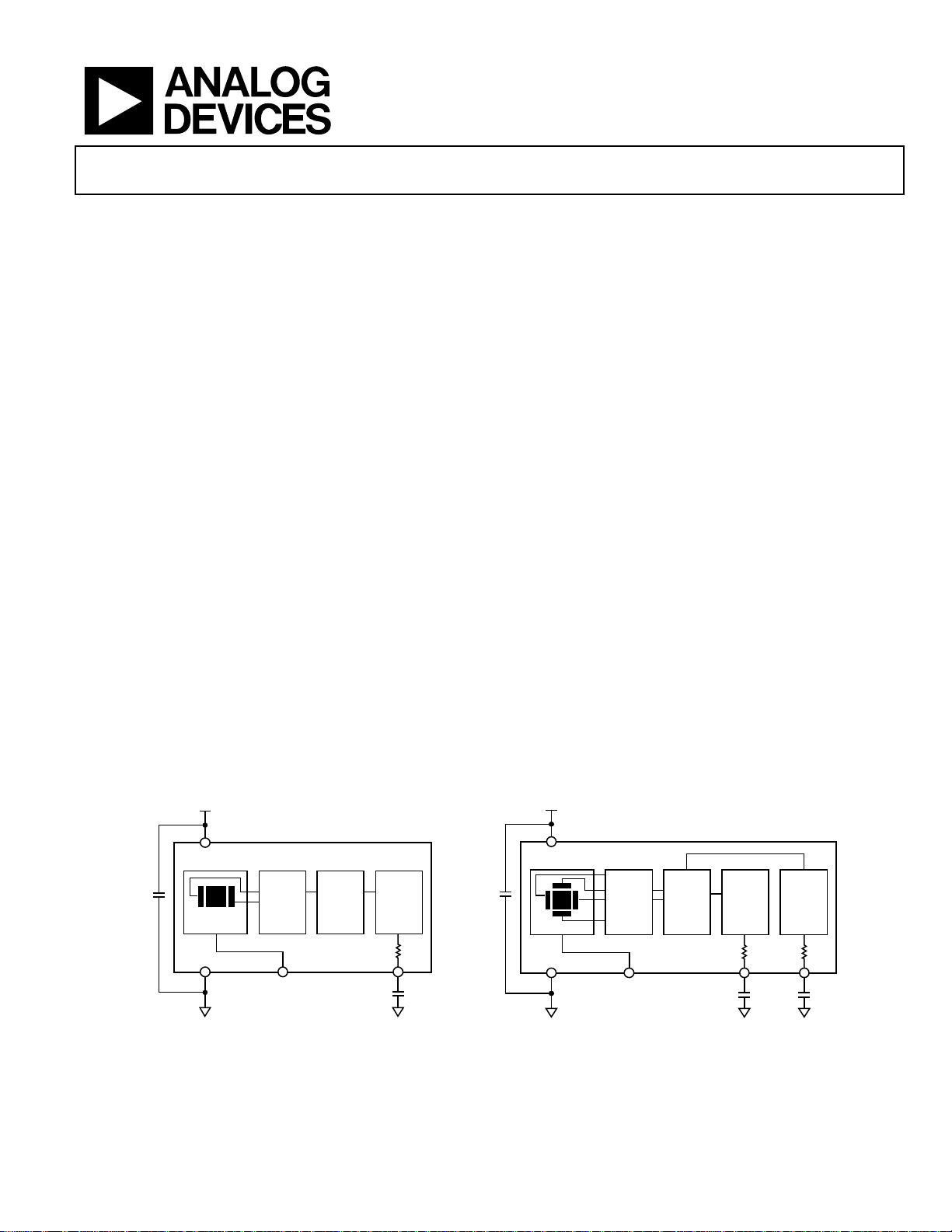
GENERAL DESCRIPTION
The ADXL103/ADXL203 are high precision, low power, complete
single- and dual-axis accelerometers with signal conditioned
voltage outputs, all on a single, monolithic IC. The ADXL103/
ADXL203 measure acceleration with a full-scale range of ±1.7 g,
±5 g, or ±18 g. The ADXL103/ADXL203 can measure both
dynamic acceleration (for example, vibration) and static
acceleration (for example, gravity).
The typical noise floor is 110 μg/√Hz, allowing signals below 1 mg
(0.06° of inclination) to be resolved in tilt sensing applications
using narrow bandwidths (<60 Hz).
The user selects the bandwidth of the accelerometer using
Capacitor C
Bandwidths of 0.5 Hz to 2.5 kHz can be selected to suit the
application.
The ADXL103 and ADXL203 are available in a 5 mm × 5 mm ×
2 mm, 8-terminal ceramic LCC package.
and Capacitor CY at the X
X
OUT
and Y
OUT
pins.
FUNCTIONAL BLOCK DIAGRAMS
+5V
V
S
ADXL103
C
DC
SENSOR
COM ST X
Rev. D
Information furnished by Analog Devices is believed to be accurate and reliable. However, no
responsibility is assumed by Anal og Devices for its use, nor for any infringements of patents or ot her
rights of third parties that may result from its use. Specifications subject to change without notice. No
license is granted by implication or otherwise under any patent or patent rights of Analog Devices.
Trademarks and registered trademarks are the property of their respective owners.
AC
AMP
DEMOD
R
FILT
32kΩ
OUTPUT
AMP
C
OUT
X
+5V
V
S
ADXL203
C
DC
SENSOR
COM ST Y
Figure 1.
One Technology Way, P.O. Box 9106, Norwood, MA 02062-9106, U.S.A.
Tel: 781.329.4700 www.analog.com
Fax: 781.461.3113 ©2004–2011 Analog Devices, Inc. All rights reserved.
AC
AMP
DEMOD
R
FILT
32kΩ
OUTPUT
AMP
C
OUT
Y
OUTPUT
R
FILT
32kΩ
AMP
X
OUT
C
X
03757-001

ADXL103/ADXL203 Data Sheet
TABLE OF CONTENTS
Features.............................................................................................. 1
Applications....................................................................................... 1
General Description......................................................................... 1
Functional Block Diagrams............................................................. 1
Specifications..................................................................................... 3
Absolute Maximum Ratings............................................................ 4
ESD Caution.................................................................................. 4
Pin Configurations and Function Descriptions........................... 5
Typical Performance Characteristics............................................. 6
ADXL103 and ADXL203............................................................. 6
AD22293........................................................................................ 9
AD22035 and AD22037 ............................................................ 10
All Models ...................................................................................12
Theory of Operation ......................................................................13
Performance................................................................................ 13
Applications Information.............................................................. 14
Power Supply Decoupling......................................................... 14
Setting the Bandwidth Using CX and CY................................. 14
Self Test........................................................................................ 14
Design Trade-Offs for Selecting Filter Characteristics: The
Noise/Bandwidth Trade-Off..................................................... 14
Using the ADXL103/ADXL203 with Operating Voltages
Other than 5 V............................................................................ 15
Using the ADXL203 as a Dual-Axis Tilt Sensor ........................ 15
Outline Dimensions....................................................................... 16
Ordering Guide .......................................................................... 16
Automotive Products ................................................................. 16
REVISION HISTORY
9/11—Rev. C to Rev. D
Added AD22293, AD22035, and AD22037............... Throughout
Changes to Application Section and General Description
Section................................................................................................ 1
Changes to Table 1............................................................................ 3
Deleted Figure 13 and Figure 14: Renumbered Sequentially ..... 7
Deleted Figure 17 and Figure 22..................................................... 8
Added Figure 19 to Figure 24; Renumbered Sequentially .......... 9
Added Figure 25 to Figure 34........................................................10
Added All Models Section, Figure 35 to Figure 38.................... 12
Changes to Figure 39...................................................................... 13
Changes to Ordering Guide.......................................................... 16
Changes to Automotive Products Section................................... 16
5/10—Rev. B to Rev. C
Changes to Figure 24 Caption....................................................... 12
Added Automotive Products Section .......................................... 12
4/10—Rev. A to Rev. B
Changes to Features Section............................................................1
Updated Outline Dimensions....................................................... 12
Changes to Ordering Guide.......................................................... 12
2/06—Rev. 0 to Rev. A
Changes to Features..........................................................................1
Changes to Table 1.............................................................................3
Changes to Figure 2...........................................................................4
Changes to Figure 3 and Figure 4....................................................5
Changes to the Performance Section..............................................9
4/04—Revision 0: Initial Version
Rev. D | Page 2 of 16

Data Sheet ADXL103/ADXL203
SPECIFICATIONS
TA = −40°C to +125°C, VS = 5 V, CX = CY = 0.1 μF, acceleration = 0 g, unless otherwise noted. All minimum and maximum specifications
are guaranteed. All typical specifications are not guaranteed.
Table 1.
ADXL103/ADXL203 AD22293 AD22035/AD22037
Parameter Test Conditions Min Typ Max Min Typ Max Min Typ Max Unit
SENSOR Each axis
Measurement Range1 ±1.7 ±5 ±6 ±18
Nonlinearity % of full scale ±0.2 ±1.25 ±0.2 ±1.25 ±0.2 ±1.25 %
Package Alignment Error ±1 ±1 ±1 Degrees
Alignment Error (ADXL203) X to Y sensor ±0.1 ±0.1 ±0.1 Degrees
Cross-Axis Sensitivity ±1.5 ±3 ±1.5 ±3 ±1.5 ±3 %
SENSITIVITY (RATIOMETRIC)2 Each axis
Sensitivity at X
Sensitivity Change Due to
Temperature
, Y
V
OUT
OUT
3
= 5 V 960 1000 1040 293 312 331 94 100 106 mV/g
S
VS = 5 V ±0.3 ±0.3 ±0.3
ZERO g BIAS LEVEL (RATIOMETRIC) Each axis
0 g Voltage at X
Initial 0 g Output Deviation
, Y
V
OUT
OUT
= 5 V 2.4 2.5 2.6 2.4 2.5 2.6 2.4 2.5 2.6 V
S
V
= 5 V, 25°C ±25 ±50 ±125 mg
S
From Ideal
0 g Offset vs. Temperature ±0.1 ±0.8 ±0.3 ±1.8 ±1 mg/°C
NOISE
Output Noise <4 kHz, VS = 5 V 1 3 1 3 2 mV rms
Noise Density 110 200 130
FREQUENCY RESPONSE4
CX, CY Range5 0.002 10 0.002 10 0.002 10 μF
R
Tolerance 24 32 40 24 32 40 24 32 40 kΩ
FILT
Sensor Resonant Frequency 5.5 5.5 5.5 kHz
SELF TEST6
Logic Input Low 1 1 1 V
Logic Input High 4 4 4 V
ST Input Resistance to GND 30 50 30 50 30 50 kΩ
Output Change at X
, Y
ST 0 to ST 1 450 750 1100 125 250 375 60 80 100 mV
OUT
OUT
OUTPUT AMPLIFIER
Output Swing Low No load 0.05 0.2 0.05 0.2 0.05 0.2 V
Output Swing High No load 4.5 4.8 4.5 4.8 4.5 4.8 V
POWER SUPPLY (VDD)
Operating Voltage Range 3 6 3 6 3 6 V
Quiescent Supply Current 0.7 1.1 0.7 1.1 0.7 1.1 mA
Turn-On Time7 20 20 20 ms
1
Guaranteed by measurement of initial offset and sensitivity.
2
Sensitivity is essentially ratiometric to VS. For VS = 4.75 V to 5.25 V, sensitivity is 186 mV/V/g to 215 mV/V/g.
3
Defined as the output change from ambient-to-maximum temperature or ambient-to-minimum temperature.
4
Actual frequency response controlled by user-supplied external capacitor (CX, CY).
5
Bandwidth = 1/(2 × π × 32 kΩ × C). For CX, CY = 0.002 μF, bandwidth = 2500 Hz. For CX, CY = 10 μF, bandwidth = 0.5 Hz. Minimum/maximum values are not tested.
6
Self-test response changes cubically with VS.
7
Larger values of CX, CY increase turn-on time. Turn-on time is approximately 160 × CX or CY + 4 ms, where CX, CY are in μF.
g
%
μg/√Hz
rms
Rev. D | Page 3 of 16
ADXL103/ADXL203 Data Sheet
ABSOLUTE MAXIMUM RATINGS
Table 2.
Parameter Rating
Acceleration (Any Axis, Unpowered) 3500 g
Acceleration (Any Axis, Powered) 3500 g
Drop Test (Concrete Surface) 1.2 m
VS −0.3 V to +7.0 V
All Other Pins
Output Short-Circuit Duration
(COM − 0.3 V) to
(V
+ 0.3 V)
S
Indefinite
(Any Pin to Common)
Temperature Range (Powered) −55°C to +125°C
Temperature Range (Storage) −65°C to +150°C
Stresses above those listed under Absolute Maximum Ratings
may cause permanent damage to the device. This is a stress rating
only; functional operation of the device at these or any other
conditions above those indicated in the operational section of
this specification is not implied. Exposure to absolute maximum
rating conditions for extended periods may affect device reliability.
T
P
T
L
T
SMAX
RAMP-UP
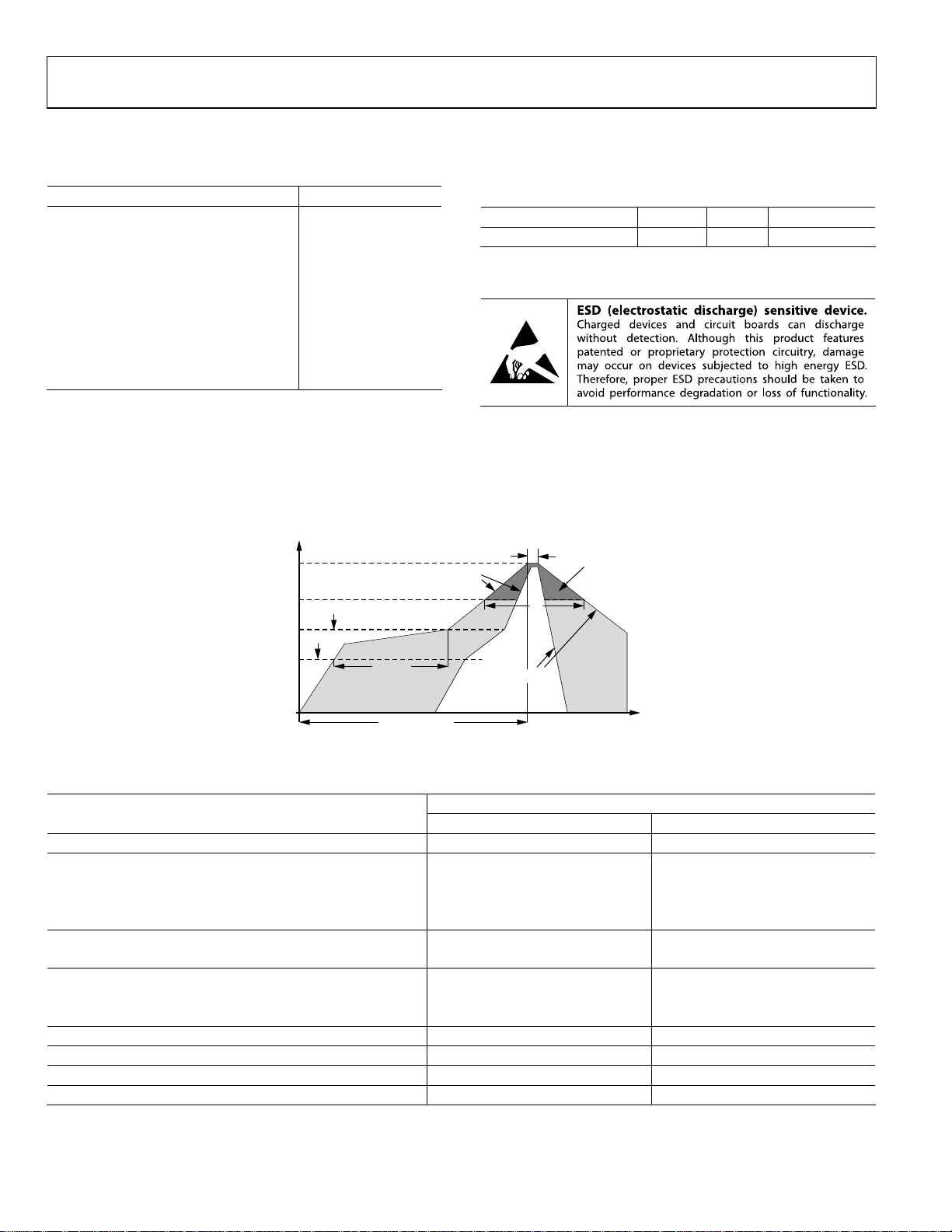
Table 3. Package Characteristics
Package Type θJA θ
Device Weight
JC
8-Terminal Ceramic LCC 120°C/W 20°C/W <1.0 gram
ESD CAUTION
CRITICAL ZONE
TO T
t
P
T
L
P
t
L
T
SMIN
TEMPERAT URE
t
S
PREHEAT
t
25°C TO PE AK
Figure 2. Recommended Soldering Profile
RAMP-DOWN
TIME
03757-102
Table 4. Solder Profile Parameters
Test Condition
Profile Feature Sn63/Pb37 Pb-Free
Average Ramp Rate (TL to TP) 3°C/second maximum 3°C/second maximum
Preheat
Minimum Temperature (T
Maximum Temperature (T
Time (T
T
to TL
SMAX
SMIN
to T
) (tS) 60 seconds to 120 seconds 60 seconds to 150 seconds
SMAX
) 100°C 150°C
SMIN
) 150°C 200°C
SMAX
Ramp-Up Rate 3°C/second 3°C/second
Time Maintained above Liquidous (TL)
Liquidous Temperature (TL) 183°C 217°C
Time (tL) 60 seconds to 150 seconds 60 seconds to 150 seconds
Peak Temperature (TP) 240°C + 0°C/−5°C 260°C + 0°C/−5°C
Time Within 5°C of Actual Peak Temperature (tP) 10 seconds to 30 seconds 20 seconds to 40 seconds
Ramp-Down Rate 6°C/second maximum 6°C/second maximum
Time 25°C to Peak Temperature 6 minutes maximum 8 minutes maximum
Rev. D | Page 4 of 16
Data Sheet ADXL103/ADXL203
.
.
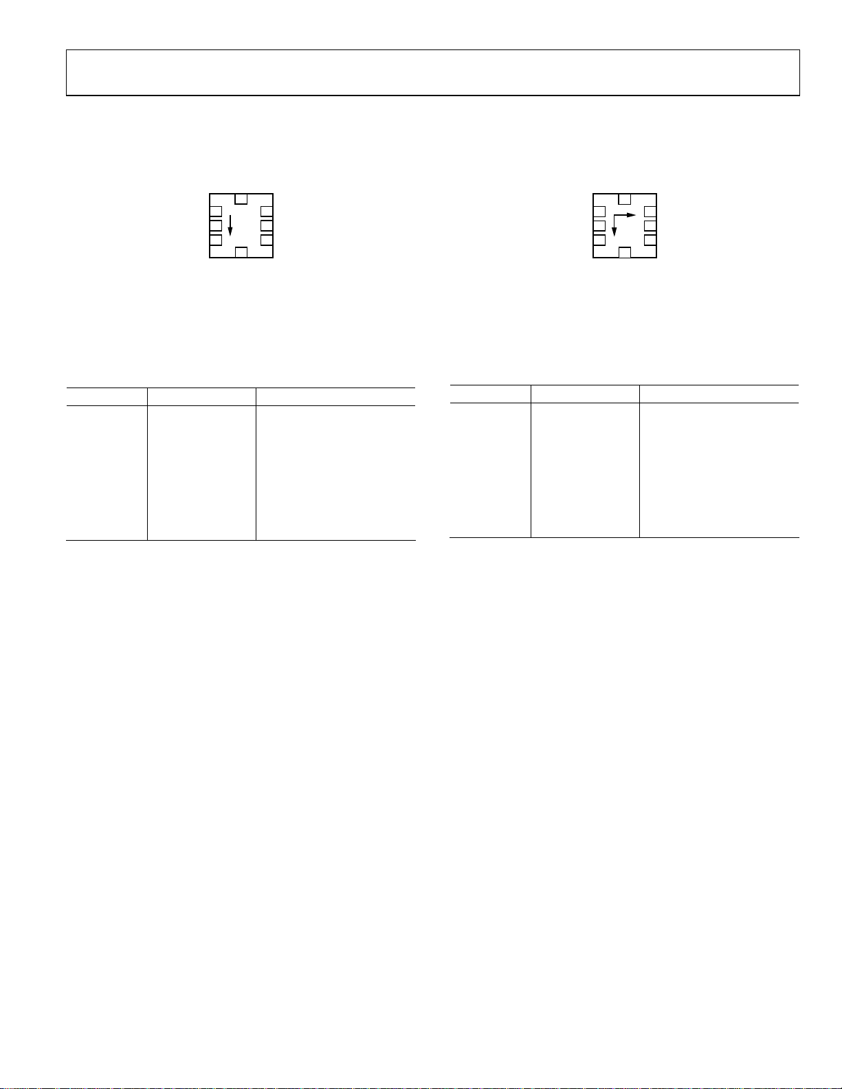
PIN CONFIGURATIONS AND FUNCTION DESCRIPTIONS
ADXL103
TOP VIEW
(Not to Scale)
V
S
8
1
ST
NC
2
COM
3
NOTES
1. NC = NO CONNECT . DO NOT CONNECT TO THIS PI N
Figure 3. ADXL103 Pin Configuration
7
X
+X
4
NC
OUT
6
NC
5
NC
03757-002
NOTES
1. NC = NO CONNECT . DO NOT CONNECT TO THIS PIN
Figure 4. ADXL203 Pin Configuration
ST
NC
COM
ADXL203
TOP VIEW
(Not to Scale)
V
S
8
1
+Y
2
+X
3
4
NC
7
X
OUT
6
Y
OUT
5
NC
03757-003
Table 5. ADXL103 Pin Function Descriptions
Pin No. Mnemonic Description
1 ST Self Test
2 NC Do Not Connect
3 COM Common
4 NC Do Not Connect
5 NC Do Not Connect
6 NC Do Not Connect
7 X
X Channel Output
OUT
8 VS 3 V to 6 V
Table 6. ADXL203 Pin Function Descriptions
Pin No. Mnemonic Description
1 ST Self Test
2 NC Do Not Connect
3 COM Common
4 NC Do Not Connect
5 NC Do Not Connect
6 Y
7 X
Y Channel Output
OUT
X Channel Output
OUT
8 VS 3 V to 6 V
Rev. D | Page 5 of 16
 Loading...