Analog Devices ADXL05JH, ADXL05AH Datasheet
61 g to 65 g Single Chip Accelerometer
a
FEATURES
g
5 milliNoise Level 123 Less than the ADXL50
User Selectable Full Scale from 61 g to 65
Output Scale Selectable from 200 mV/g to 1 V/
Complete Acceleration Measurement System on a
Self Test on Digital Command
+5 V Single Supply Operation
1000
APPLICATIONS
Low Cost Sensor for Vibration Measurement
Tilt Sensing with Faster Response than Electrolytic or
More Sensitive Alarms and Motion Detectors
Affordable Inertial Sensing of Velocity and Position
GENERAL DESCRIPTION
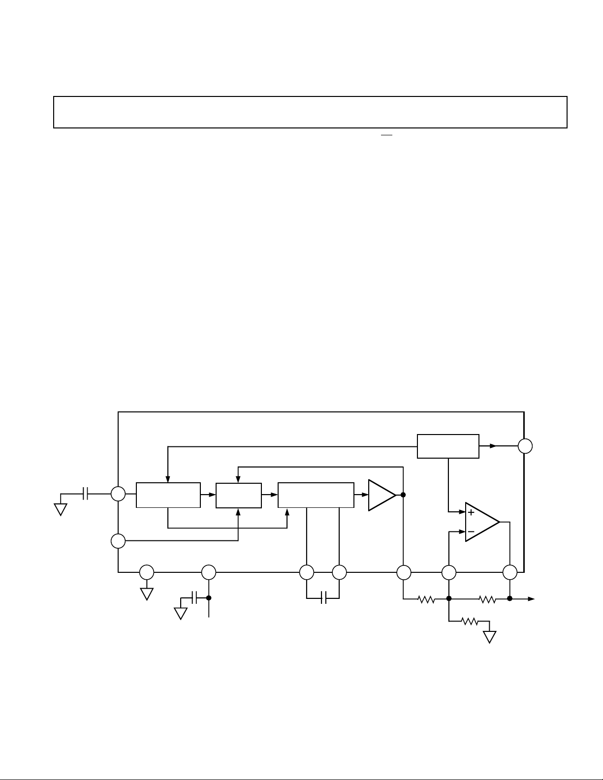
The ADXL05 is a complete acceleration measurement system
on a single monolithic IC. The ADXL05 will measure accelerations with full-scale ranges of ±5 g to ±1 g or less. Typical noise
Resolution
Single Chip IC
g
Shock Survival
Mercury Sensors
g
g
with Signal Conditioning
ADXL05*
floor is 500 µg/√Hz, (12× less than the ADXL50), allowing signals below 5 milli-g to be resolved. The ADXL05 is a force balanced capacitive accelerometer with the capability to measure
both ac accelerations (typical of vibration) or dc accelerations
(such as inertial force or gravity). Three external capacitors and
a +5 volt regulated power supply are all that is required to
measure accelerations up to ±5 g. Three resistors are used to
configure the output buffer amplifier to set scale factors from
200 mV/g to 1 V/g. External capacitors may be added to the
resistor network to provide 1 or 2 poles of filtering. No additional active components are required to interface directly to
most analog to digital converters (ADCs).
The device features a TTL compatible self-test function that
can electrostatically deflect the sensor beam at any time to verify
that the sensor and its electronics are functioning correctly.
The ADXL05 is available in a hermetic 10-pin TO-100 metal
can, specified over the 0°C to +70°C commercial, and –40°C to
+85°C industrial temperature ranges. Contact factory for availability of automotive grade devices.
OSCILLATOR
DECOUPLING
CAPACITOR
C2
SELF-TEST
(ST)
*Patents pending.
4
7
COM
ADXL05
OSCILLATOR
C3
+5V
15
FUNCTIONAL BLOCK DIAGRAM
SENSOR
DEMODULATOR
C1
DEMODULATOR
CAPACITOR
32
C1
PREAMP
V
PR
8
REFERENCE
10
R1
+1.8V
V
IN–
BUFFER
AMP
R3
R2
+3.4V
V
REF
6
OUTPUT
9
V
OUT
REV. B
Information furnished by Analog Devices is believed to be accurate and
reliable. However, no responsibility is assumed by Analog Devices for its
use, nor for any infringements of patents or other rights of third parties
which may result from its use. No license is granted by implication or
otherwise under any patent or patent rights of Analog Devices.
© Analog Devices, Inc., 1996
One Technology Way, P.O. Box 9106, Norwood. MA 02062-9106, U.S.A.
Tel: 617/329-4700 Fax: 617/326-8703

ADXL05–SPECIFICA TIONS
(TA = T
MIN
to T
, TA = +258C for J Grade Only, VS = +5 V, @ Acceleration = 0 g,
MAX
unless otherwise noted)
Parameter Conditions Min Typ Max Units
ADXL05J/A
SENSOR INPUT
Measurement Range Guaranteed Full Scale –5 +5 g
Nonlinearity Best Fit Straight Line, 5 g FS 0.2 % of FS
Alignment Error
Transverse Sensitivity
1
2
± 1 Degrees
± 2%
SENSITIVITY
Initial Sensitivity at V
Initial Sensitivity at V
Temperature Drift
PR
OUT
3
ZERO g BIAS LEVEL at V
Initial Offset 1.50 1.80 2.10 V
vs. Temperature
3
+25°C 175 200 225 mV/g
+25°C, R3/R1 = 5 0.875 1.000 1.125 V/g
± 0.5 % of Reading
PR
± 25/40 mV
vs. Supply VS = 4.75 V to 5.25 V 10 32 mV/V
NOISE PERFORMANCE at V
PR
Voltage Noise Density BW = 4 Hz to 1 kHz 500 1000 µg/√Hz
Noise in 100 Hz Bandwidth 5mg rms
Noise in 10 Hz Bandwidth 1.6 mg rms
FREQUENCY RESPONSE
3 dB Bandwidth
3 dB Bandwidth
4
4
C1 = 0.022 µF (See Figure 9) 1000 1600 Hz
C1 = 0.010 µF 4 kHz
Sensor Resonant Frequency 12 kHz
SELF TEST INPUT
Output Change at V
5
PR
ST Pin from Logic “0” to “1” –0.85 –1.00 –1.15 V
Logic “1” Voltage 2.0 V
Logic “0” Voltage 0.8 V
Input Resistance To Common 50 kΩ
+3.4 V REFERENCE
Output Voltage 3.350 3.400 3.450 V
Output Temperature Drift
3
±5mV
Power Supply Rejection DC, VS = +4.75 V to +5.25 V 1 10 mV/V
Output Current Sourcing 500 µA
PREAMPLIFIER OUTPUT
Voltage Swing 0.25 VS – 1.4 V
Current Output Source or Sink 30 80 µA
Capacitive Load Drive 100 pF
BUFFER AMPLIFIER
Input Offset Voltage
6
Delta from Nominal 1.800 V ±10 ±25 mV
Input Bias Current 520nA
Open-Loop Gain DC 80 dB
Unity Gain Bandwidth 200 kHz
Output Voltage Swing I
= ±100 µA 0.25 VS – 0.25 V
OUT
Capacitive Load Drive 1000 pF
Power Supply Rejection DC, VS = +4.75 V to +5.25 V 1 10 mV/V
POWER SUPPLY
Operating Voltage Range 4.75 5.25 V
Quiescent Supply Current 8.0 10.0 mA
TEMPERATURE RANGE
Operating Range J 0 +70 °C
Specified Performance A –40 +85 °C
Automotive Grade* –40 +125 °C
NOTES
1
Alignment error is specified as the angle between the true and indicated axis of sensitivity, (see Figure 2).
2
Transverse sensitivity is measured with an applied acceleration that is 90° from the indicated axis of sensitivity. Transverse sensitivity is specified as the percent of
transverse acceleration that appears at the V
3
Specification refers to the maximum change in parameter from its initial at +25°C to its worst case value at T
4
Frequency at which response is 3 dB down from dc response assuming an exact C1 value is used. Maximum recommended BW is 6 kHz using a 0.010 µF capacitor, refer to
Figure 9.
5
Applying logic high to the self-test input has the effect of applying an acceleration of –5 g to the ADXL05.
6
Input offset voltage is defined as the output voltage differential from 1.800 V when the amplifier is connected as a follower. The voltage at this pin has a temperature drift
proportional to that of the 3.4 V reference.
*Contact factory for availability of automotive grade devices.
All min and max specifications are guaranteed. Typical specifications are not tested or guaranteed.
Specifications subject to change without notice.
output. This is the algebraic sum of the alignment and the inherent sensor sensitivity errors, (see Figure 2).
PR
MIN
to T
MAX
.
–2–
REV. B
System Performance Specifications–ADXL05
0.022µF
0.022µF
COM
C2
4
ADXL05
C1
C1
2
3
5
+3.4V
REF
6
PRE-AMP
8
V
PR
C4
1.8V
10
V
R1
IN–
R2
BUFFER
AMP
R3
1
+5V
C3
0.1µF
9
V
OUT
NOMINAL VALUES:
R1 = 49.9kΩ
R3 = 249kΩ
R2 = 640kΩ
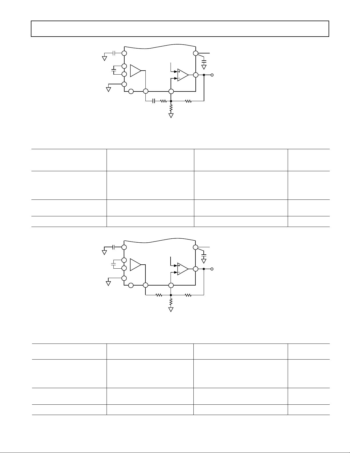
AC COUPLED CONNECTION (61.5 g Full Scale)
(@ V
Terminal (Pin 9), unless otherwise noted. 0 g Bias Level = +2.5 V, C1 = 0.022 mF, R2 = 2.57 R3
OUT
ADXL05J/A
Parameter Conditions Min Typ Max Units
Buffer Gain G = R3/R1* 5
FULL-SCALE RANGE –1.5 +1.5 g
SENSITIVITY @
Temperature Drift T
ZERO g BIAS LEVEL @ +25°C 2.5 V
Temperature Drift +25°C to T
FREQUENCY RESPONSE C4 = 3.3 µF, R1 = 49.9 kΩ 1 1000 Hz
*Note: Resistor tolerance will affect system accuracy. Use of ±1% (or better) metal film resistors is recommended.
+25°C 875 1000 1,125 mV/g
MIN
to T
MAX
MIN
or T
MAX
±0.5 % of Reading
2/5 mV
0.022µF
0.022µF
COM
C2
4
ADXL05
C1
C1
2
3
5
+3.4V
REF
6
PRE-AMP
8
V
PR
1.8V
10
V
R1
IN–
R2
BUFFER
AMP
R3
1
+5V
C3
0.1µF
9
V
OUT
NOMINAL VALUES:
R1 = 49.9kΩ
R3 = 100kΩ (G=2)
R2 = 255kΩ (G=2)
DC COUPLED CONNECTION (62 g Full Scale)
(@ V
Terminal (Pin 9), unless otherwise noted. 0 g Bias Level = +2.5 V, C1 = 0.022 mF, R2 = 2.57 R3)
OUT
ADXL05J/A
Parameter Conditions Min Typ Max Units
Buffer Gain G = R3/R1* 2
FULL-SCALE RANGE –2 +2 g
SENSITIVITY @
Temperature Drift T
ZERO g BIAS LEVEL @ +25°C 1.75 2.5 3.2 V
Temperature Drift +25°C to T
FREQUENCY RESPONSE dc 1000 Hz
*Note: Resistor tolerance will affect system accuracy. Use of ±1% (or better) metal film resistors is recommended.
+25°C 350 400 450 mV/g
MIN
to T
MAX
MIN
or T
MAX
±0.5 % of Reading
±50/80 mV
REV. B
–3–
ADXL05
WARNING!
ESD SENSITIVE DEVICE
ABSOLUTE MAXIMUM RATINGS*
Acceleration (Any Axis, Unpowered for 0.5 ms) . . . . . . 1000 g
Acceleration (Any Axis, Powered for 0.5 ms) . . . . . . . . . . 500 g
+V
. . . . . . . . . . . . . . . . . . . . . . . . . . . . . . . . –0.3 V to +7.0 V
S
Package Characteristics
Package u
JA
10-Pin TO-100 130°C/W 30°C/W 5 Grams
Output Short Circuit Duration
(V
, V
, V
PR
OUT
Operating Temperature . . . . . . . . . . . . . . . . .–55°C to +125°C
Storage Temperature . . . . . . . . . . . . . . . . . . .–65°C to +150°C
*Stresses above those listed under “Absolute Maximum Ratings” may cause
permanent damage to the device. This is a stress rating only; the functional
operation of the device at these or any other conditions above those indicated in the
Terminals to Common) . . . . . . .Indefinite
REF
ORDERING GUIDE
Model Temperature Range
ADXL05JH 0°C to +70°C
ADXL05AH –40°C to +85°C
operational sections of this specification is not implied. Exposure to absolute
maximum rating conditions for extended periods may affect device reliability.
CAUTION
ESD (electrostatic discharge) sensitive device. Electrostatic charges as high as 4000 V readily
accumulate on the human body and test equipment and can discharge without detection.
Although the ADXL05 features proprietary ESD protection circuitry, permanent damage may
occur on devices subjected to high energy electrostatic discharges. Therefore, proper ESD
precautions are recommended to avoid performance degradation or loss of functionality.
Drops onto hard surfaces can cause shocks of greater than 1000 g
and exceed the absolute maximum rating of the device. Care
should be exercised in handling to avoid damage.
u
JC
Device Weight
PIN DESCRIPTION
+5 V The power supply input pin.
C2 Connection for an external bypass capacitor (nominally 0.022 µF)
C1 Connections for the demodulator capacitor, nominally 0.022 µF.
COM The power supply common (or “ground”) connection.
V
ST The digital self-test input. It is both CMOS and TTL compatible.
V
V
V
used to prevent oscillator switching noise from interfering with
other ADXL05 circuitry. Please see the section on component
selection.
See the section on component selection for application information.
Output of the internal 3.4 V voltage reference.
REF
The ADXL05 preamplifier output providing an output voltage of
PR
200 mV per g of acceleration.
Output of the buffer amplifier.
OUT
The inverting input of the uncommitted buffer amplifier.
IN–
CONNECTION DIAGRAM
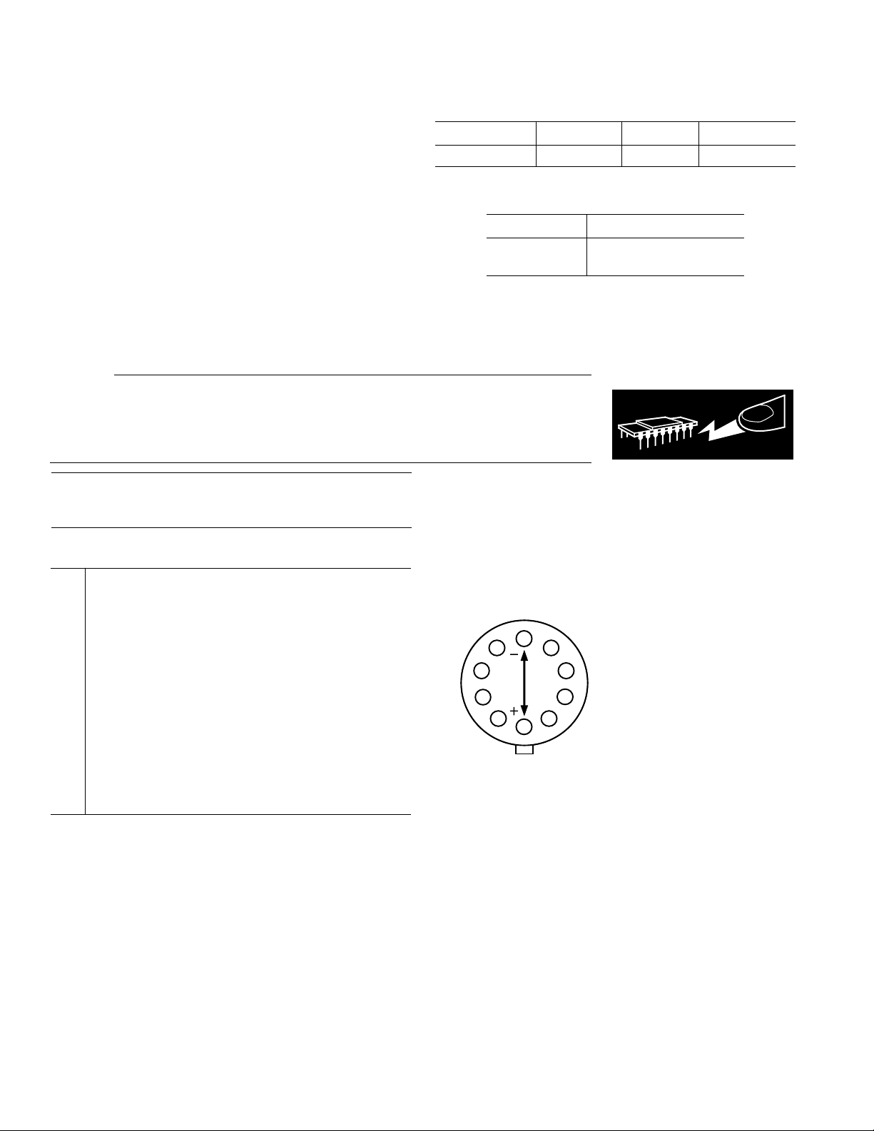
10-Header (TO-100)
TOP VIEW
OUT
COM
6
6
7
7
AXIS OF
AXIS OF
8
8
9
9
5
5
SENSITIVITY
SENSITIVITY
10
10
V
IN–
C2
4
4
C1
3
3
2
2
1
1
+5V
NOTES:
C1
AXIS OF SENSITIVITY IS ALONG A LINE
BETWEEN PIN 5 AND THE TAB.
THE CASE OF THE METAL CAN
PACKAGE IS CONNECTED TO PIN 5
(COMMON).
ARROW INDICATES DIRECTION OF
POSITIVE ACCELERATION ALONG AXIS
OF SENSITIVITY.
V
REF
ST
V
PR
V
–4–
REV. B
ADXL05
+1g
INDICATED POLARITY IS THAT
OCCURRING AT V
PR
.
TAB
PIN 5
+
–
GLOSSARY OF TERMS
Acceleration: Change in velocity per unit time.
Acceleration Vector: Vector describing the net acceleration
acting upon the ADXL05 (A
XYZ
).
g: A unit of acceleration equal to the average force of gravity
occurring at the earth’s surface. A g is approximately equal to
32.17 feet/s
2
, or 9.807 meters/s2.
Nonlinearity: The maximum deviation of the ADXL05 output
voltage from a best fit straight line fitted to a plot of acceleration
vs. output voltage, calculated as a % of the full-scale output
voltage (@ 5 g).
Resonant Frequency: The natural frequency of vibration of
the ADXL05 sensor’s central plate (or “beam”). At its resonant
frequency of 12 kHz, the ADXL05’s moving center plate has a
peak in its frequency response with a Q of 3 or 4.
Sensitivity: The output voltage change per g unit of accelera-
tion applied, specified at the V
pin in mV/g.
PR
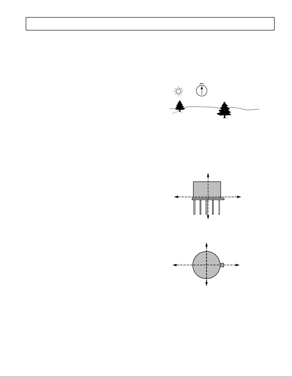
Sensitive Axis (X): The most sensitive axis of the accelerometer sensor. Defined by a line drawn between the package tab
and Pin 5 in the plane of the pin circle. See Figures 2a and 2b.
Sensor Alignment Error: Misalignment between the
ADXL05’s on-chip sensor and the package axis, defined by
Pin 5 and the package tab.
Total Alignment Error: Net misalignment of the ADXL05’s
on-chip sensor and the measurement axis of the application.
This error includes errors due to sensor die alignment to the
package, and any misalignment due to installation of the sensor
package in a circuit board or module.
Transverse Acceleration: Any acceleration applied 90° to the
axis of sensitivity.
Transverse Sensitivity Error: The percent of a transverse acceleration that appears at the V
output. For example, if the
PR
transverse sensitivity is 1%, then a +10 g transverse acceleration
will cause a 0.1 g signal to appear at V
(1% of 10 g). Trans-
PR
verse sensitivity can result from a sensitivity of the sensor to
transverse forces or from misalignment of the internal sensor to
its package.
Transverse Y Axis: The axis perpendicular (90°) to the pack-
age axis of sensitivity in the plane of the package pin circle. See
Figure 2.
Transverse Z Axis: The axis perpendicular (90°) to both the
package axis of sensitivity and the plane of the package pin
circle. See Figure 2.
Polarity of the Acceleration Output
The polarity of the ADXL05 output is shown in the Figure 1.
When oriented to the earth’s gravity (and held in place), the
ADXL05 will experience an acceleration of +1 g. This corresponds to a change of approximately +200 mV at the V
PR
output pin. Note that the polarity will be reversed to a negative
going signal at the buffer amplifier output V
, due to its
OUT
inverting configuration.
Figure 1. Output Polarity at V
PR
Acceleration Vectors in Three Dimensions
The ADXL05 is a sensor designed to measure accelerations that
result from an applied force. The ADXL05 responds to the
component of acceleration on its sensitive X axis. Figures 2a
and 2b show the relationship between the sensitive “X” axis and
the transverse “Z” and “Y” axes as they relate to the TO-100
Z
SIDE VIEW
X
PIN 5
TRANSVERSE Z AXIS
TAB
Z
X
SENSITIVE (X) AXIS
Figure 2a. Sensitive X and Transverse Z Axis
Y
TOP VIEW
X
PIN 5
TRANSVERSE Y AXIS
SENSITIVE (X) AXIS
TAB
X
REV. B
Y
Figure 2b. Sensitive X and Transverse Y Axis
–5–
ADXL05
10
90
100
0%
0.5ms
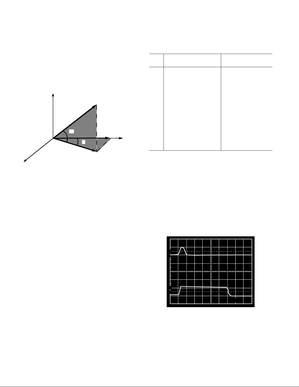
package. Figure 2c describes a three dimensional acceleration
vector (A
component of interest. To determine A
of acceleration in the XY plane (A
) which might act on the sensor, where AX is the
XYZ
, first, the component
X
) is found using the cosine
XY
law:
A
= A
XY
A
Therefore: Nominal V
–Z AXIS
Y AXIS
(cosθXY) then
XYZ
= AXY (cosθX)
X
= 200 mV/g (A
PR
θxy
θx
Axy
) (cosθXY) cosθ
XYZ
Axyz
Ax
X
X AXIS
Figure 2c. A Vector Analysis of an Acceleration Acting
Upon the ADXL05 in Three Dimensions
Note that an ideal sensor will react to forces along or at angles
to its sensitive axis but will reject signals from its various transverse axes, i.e., those exactly 90° from the sensitive “X” axis.
But even an ideal sensor will produce output signals if the transverse signals are not exactly 90° to the sensitive axis. An acceleration that is acting on the sensor from a direction different
from the sensitive axis will show up at the ADXL05 output at a
reduced amplitude.
Table I shows the percentage signals resulting from various θ
X
angles. Note that small errors in alignment have a negligible
effect on the output signal. A 1° error will only cause a 0.02%
error in the signal. Note, however, that a signal coming 1° off of
the transverse axis (i.e., 89° off the sensitive axis) will still contribute 1.7% of its signal to the output. Thus large transverse
signals could cause output signals as large as the signals of
interest. Table I may also be used to approximate the effect of
the ADXL05’s internal errors due to misalignment of the die to
the package. For example: a 1 degree sensor alignment error will
allow 1.7% of a transverse signal to appear at the output.
Table I. Ideal Output Signals for Off Axis Applied
Accelerations Disregarding Device Alignment and
Transverse Sensitivity Errors
% of Signal Appearing Output in gs for a 5 g
θ
X
at Output Applied Acceleration
0 100% 5.000 (On Axis)
1° 99.98% 4.999
2° 99.94% 4.997
3° 99.86% 4.993
5° 99.62% 4.981
10° 98.48% 4.924
30° 86.60% 4.330
45° 70.71% 3.536
60° 50.00% 2.500
80° 17.36% 0.868
85° 8.72% 0.436
87° 5.25% 0.263
88° 3.49% 0.175
89° 1.7% 0.085
90° 0% 0.000 (Transverse Axis)
Mounting Fixture Resonances
A common source of error in acceleration sensing is resonance
of the mounting fixture. For example, the circuit board that the
ADXL05 mounts to may have resonant frequencies in the same
range as the signals of interest. This could cause the signals
measured to be larger than they really are. A common solution
to this problem is to dampen these resonances by mounting the
ADXL05 near a mounting post or by adding extra screws to
hold the board more securely in place.
When testing the accelerometer in your end application, it is
recommended that you test the application at a variety of frequencies in order to ensure that no major resonance problems
exist (refer to Analog Devices Application Note AN-379).
Figure 3. 500 g Shock Overload Recovery. Top Trace, PCB
Reference Accelerometer Output: 500 g/Vertical Division.
Bottom Trace, ADXL05 Output at V
–6–
PR
REV. B
 Loading...