

3 GHz HDMI Receiver
ADV7619
Rev. B
Trademarks and registered trademarks are the prop erty of their respective owner s.
Fax: 781.461.3113 ©2011–2012 Analog Devices, Inc. All rights reserved.
TMDS
DDC
TMDS
DDC
COMPONENT
PROCESSOR
HS/VS
FIELD/DE
CLK
DATA
I2S
S/PDIF
DSD
HBR
MCLK
HS
VS/FIELD
DE
AUDIO
OUTPUT
MCLK
SCLK
CLK
36-/48-BIT
OUTPUT BUS
SCLK
LRCLK
36
48
OUTPUT M UX
OUTPUT M UX
HDMI1
HDMI2
ADV7619
09580-001
FAST
SWITCH
HDCP
KEYS
DEEP
COLOR
HDMI Rx
Data Sheet
FEATURES
High-Definition Multimedia Interface (HDMI®) 1.4a features
supported
All mandatory and additional 3D video formats supported
Extended colorimetry, including sYCC601, Adobe® RGB,
Adobe YCC601, xvYCC extended gamut color
CEC 1.4-compatible
HDMI 3 GHz receiver
297 MHz maximum TMDS clock frequency
Supports 4k × 2k resolution
Xpressview fast switching of HDMI ports
Up to 48-bit Deep Color with 36-/30-/24-bit support
High-bandwidth Digital Content Protection (HDCP) 1.4
support with internal HDCP keys
HDCP repeater support: up to 127 KSVs supported
Integrated CEC controller
Programmable HDMI equalizer
5 V detect and Hot Plug assert for each HDMI port
Audio support
Audio support including high bit rate (HBR) and
Direct Stream Digital (DSD)
S/PDIF (IEC 60958-compatible) digital audio support
Supports up to four I
2
S outputs
Dual Port, Xpressview,
Advanced audio mute feature
Dedicated, flexible audio output port
Super Audio CD® (SACD) with DSD output interface
HBR audio
Dolby® TrueH D
DTS-HD Master Audio™
General
Interrupt controller with 2 interrupt outputs
Standard identification (STDI) circuit
Highly flexible, 48-bit pixel output interface
36-bit output for resolutions up to 1080p Deep Color
2 × 24-bit pass-through outputs for HDMI formats
greater than 2.25 GHz
Internal EDID RAM
Any-to-any, 3 × 3 color space conversion (CSC) matrix
128-lead TQFP_EP, 14 mm × 14 mm package
APPLICATIONS
Projectors
Video conferencing
HDTV
AVR, HTiB
Soundbar
Video switch
Information furnished by Analog Devices is believed to be accurate and reliable. However, no
responsibility is assumed by Analog Devices for its use, nor for any infringements of patents or other
rights of third parties that may resul t from its use. Specifications subject to cha nge without notice. No
license is granted by implication or otherwise under any patent or patent rights of Analog Devices.
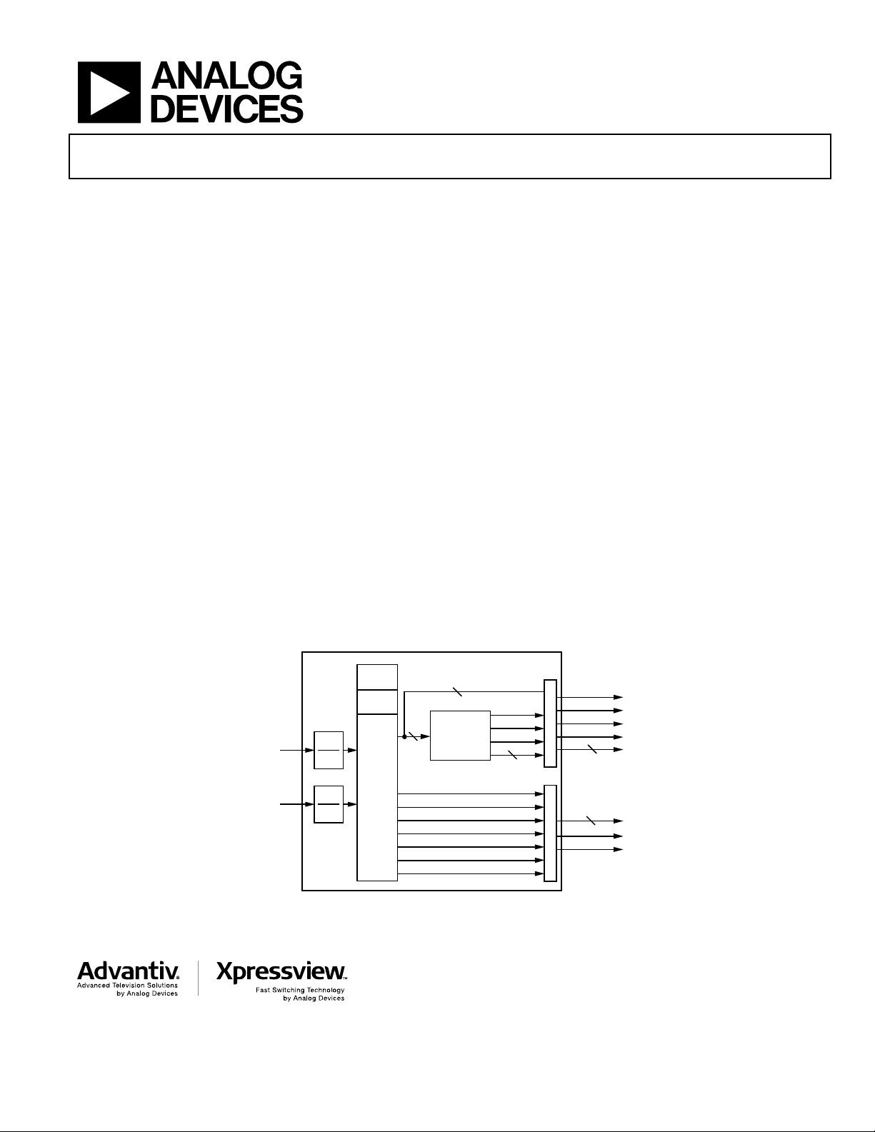
FUNCTIONAL BLOCK DIAGRAM
Figure 1.
One Technology Way, P.O. Box 9106, Norwood, MA 02062-9106, U.S.A.
Tel: 781.329.4700 www.analog.com

ADV7619 Data Sheet
TABLE OF CONTENTS
Features .............................................................................................. 1
Applications ....................................................................................... 1
Functional Block Diagram .............................................................. 1
Revision History ............................................................................... 2
General Description ......................................................................... 3
Detailed Functional Block Diagram .......................................... 3
Specifications ..................................................................................... 4
Electrical Characteristics ............................................................. 4
Data and I2C Timing Characteristics ......................................... 6
Absolute Maximum Ratings ............................................................ 8
Package Thermal Performance ................................................... 8
ESD Caution .................................................................................. 8
Pin Configuration and Function Descriptions ............................. 9
REVISION HISTORY
5/12—Rev. A to Rev. B
Changes to Features Section............................................................ 1
Changes to General Description Section and Figure 2
ange to Table 1 ............................................................................. 4
Ch
Changes to Table 3 ............................................................................ 6
Changes to Figure 5; Deleted Figure 6, Renumbered
Sequentially ....................................................................................... 7
Changes to Figure 7 .......................................................................... 9
Changes t o Tabl e 5 .......................................................................... 11
Changes to HDMI Receiver Section and Other Features
Section .............................................................................................. 14
Deleted Time-Division Multiplexed (TDM) Mode Section
and Figure 9 ..................................................................................... 15
............... 3
Power Supply Recommendations ................................................. 13
Power-Up Sequence ................................................................... 13
Power-Down Sequence .............................................................. 13
Current Rating Requirements for Power Supply Design ...... 13
Functional Overview ...................................................................... 14
HDMI Receiver ........................................................................... 14
Component Processor (CP) ...................................................... 14
Other Features ............................................................................ 14
Pixel Input/Output Formatting .................................................... 15
Pixel Data Output Mode Features ............................................ 15
Outline Dimensions ....................................................................... 22
Ordering Guide .......................................................................... 22
9/11—Rev. 0 t o R e v. A
Changes to General Description Section ...................................... 3
Changes to Data Output Transition Time Typ Values, Table 3 ... 6
Changes to Pin 113 Description ................................................... 12
Changes to Pixel Input/Output Formatting Section .................. 16
Added Endnote 1 to Tab l e 7 .......................................................... 17
Added Endnote 1 to Tab l e 1 2 ........................................................ 22
Changes to Ordering Guide .......................................................... 23
7/11—Revision 0: Initial Version
Rev. B | Page 2 of 24
Data Sheet ADV7619
09580-002
MUTE
XTALP
XTALN
SCL
SDA
CS
CEC
AP1
AP2
AP3
AP4
AP5
AP0
SCLK/INT2*
MCLK/INT2*
INT1
INT2*
P0 TO P11
P12 TO P23
P24 TO P35
P36 TO P47
LLC
HS
VS/FIELD/ALSB
DE
RXB_0±
RXB_1±
RXB_2±
RXA_0±
RXA_1±
RXA_2±
PLLs
RXA_C±
RXB_C±
DDCA_SDA
DDCA_SCL
DDCB_SDA
DDCB_SCL
HPA_A/INT2*
HPA_B
RXA_5V
RXB_5V
EQUALIZER
SAMPLER
EQUALIZER
HDCP
ENGINE
HDCP
KEYS
EDID
REPEATER
CONTROLLER
5V DETECT
AND HDP
CONTROLLER
CEC
CONTROLLER
CONTROL
INTERFACE
I
2
C
DPLL
CONTROL AND DATA
300MHz VIDEO PATH
HDMI
PROCESSOR
PACKET/
INFOFRAME
MEMORY
AUDIO
PROCESSOR
A
B
C
COMPONENT
PROCESSOR
BACK-END
COLOR
SPACE
CONVERSION
INTERRUPT
CONTROLLER
(INT1, INT2)
DATA
PREPROCESSOR
AND COLOR
SPACE
CONVERSION
PACKET
PROCESSOR
*INT2 CAN BE MADE AVAILABLE ON ONE OF THESE PINS: HPA_A/INT2, MCLK/INT2, OR SCL K/INT2.
Xpressview
FAST SWITCHI NG
SAMPLER
ADV7619
VIDEO OUTPUT FORMATTERAUDIO OUTPUT FORMATTER
GENERAL DESCRIPTION
The ADV7619 is a high quality, two input, one output (2:1)
multiplexed High-Definition Multimedia Interface (HDMI®)
receiver. The ADV7619 is offered in professional (no HDCP
keys) and commercial versions. The operating temperature
range is 0°C to 70°C.
The ADV7619 incorporates a dual input HDMI-capable
receiver that supports all mandatory 3D TV formats defined in
the HDMI 1.4a specification, HDTV formats up to 1080p 36-bit
Deep Color/2160p 8-bit, and display resolutions up to 4k × 2k
(3840 × 2160 at 30 Hz). It integrates an HDMI CEC controller
that supports the capability discovery and control (CDC) feature.
The ADV7619 incorporates Xpressview™ fast switching on both
input HDMI ports. Using the Analog Devices, Inc., hardwarebased HDCP engine to minimize software overhead, Xpressview
technology allows fast switching between both HDMI input ports
in less than 1 sec.
Each HDMI port has dedicated 5 V detect and Hot Plug™ assert
pins. The HDMI receiver also includes an integrated programmable equalizer that ensures robust operation of the interface
with long cables.
The ADV7619 offers a flexible audio output port for audio data
extraction from the HDMI stream. HDMI audio formats, including SACD via DSD and HBR, are supported by the ADV7619.
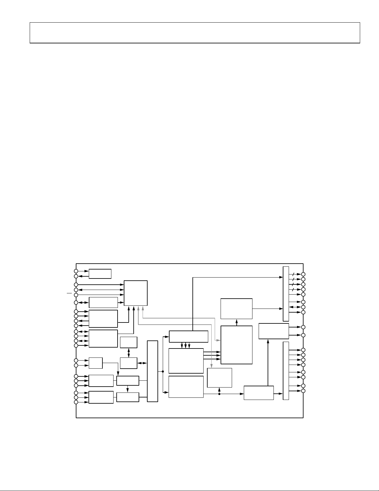
DETAILED FUNCTIONAL BLOCK DIAGRAM
The HDMI receiver has advanced audio functionality, such as
a mute controller, that prevents audible extraneous noise in the
audio output.
The ADV7619 contains one main component processor (CP),
which processes video signals from the HDMI receiver up to
1080p 36-bit Deep Color. It provides features such as contrast,
brightness and saturation adjustments, STDI detection block,
free-run, and synchronization alignment controls.
For video formats with pixel clocks higher than 170 MHz, the
video signals received on the HDMI receiver are output directly
to the pixel port output. To accommodate the higher bandwidth
required for these higher resolutions, the output on the pixel bus
consists of two 24-bit buses running at up to 150 MHz: one bus
contains the even pixels, and the other bus contains the odd
pixels. When these two buses are combined, they allow the
transfer of video data with pixel clocks up to 300 MHz. In this
mode, both 4:4:4 RGB 8-bit and 4:2:2 12-bit are supported.
Fabricated in an advanced CMOS process, the ADV7619
is provided in a 14 mm × 14 mm, 128-lead, surface-mount,
RoHS-compliant TQFP_EP package and is specified over the
0°C to 70°C temperature range.
Rev. B | Page 3 of 24
Figure 2.

ADV7619 Data Sheet
Other digital inputs
2
V
DIGITAL OUTPUTS1
Output Capacitance
C
20
pF
Digital I/O Power Supply
DVDDIO
3.14
3.3
3.46
V
Test Condition 2
10 mA
Tes t Condition 2
166 mA
Digital Core Power Supply
I
1.07 mA
SPECIFICATIONS
ELECTRICAL CHARACTERISTICS
DVDD = 1.71 V to 1.89 V, DVDDIO = 3.14 V to 3.46 V, PVDD = 1.71 V to 1.89 V, TVDD = 3.14 V to 3.46 V, CVDD = 1.71 V to 1.89 V,
operating temperature range, unless otherwise noted.
Table 1.
Parameter Symbol Test Conditions/Comments Min Typ Max Unit
DIGITAL INPUTS1
Input High Voltage VIH XTALN a nd XTALP pins 1.2 V
Input Low Voltage VIL XTALN and XTALP pins 0.4 V
Other digital inputs 0.8 V
Input Current IIN
RESET and CS pins
Other digital inputs ±10 µA
Input Capacitance CIN 10 pF
DIGITAL INPUTS (5 V TOLERANT)1
DDCA_SCL, DDCA_SDA,
DDCB_SCL, and DDCB_SDA pins
Input High Voltage VIH 2.6 V
Input Low Voltage VIL 0.8 V
Input Current IIN −70 +70 µA
±45 ±60 µA
Output High Voltage VOH 2.4 V
Output Low Voltage VOL 0.4 V
High Impedance Leakage Current I
VS/FIELD/ALSB pin ±35 ±60 µA
LEAK
HPA_A/INT2 and HPA_B pins ±70 µA
Other digital outputs ±10 µA
OUT
POWER REQUIREMENTS
Digital Core Power Supply DVDD 1.71 1.8 1.89 V
PLL Power Supply PVDD 1.71 1.8 1.89 V
Terminator Power Supply TVDD 3.14 3.3 3.46 V
Comparator Power Supply CVDD 1.71 1.8 1.89 V
CURRENT CONSUMPTION See Table 2
Digital Core Power Supply I
Test Condition 1 268 mA
DVDD
Test Condition 2 186 mA
Digital I/O Power Supply I
PLL Power Supply I
Terminator Power Supply I
Test Condition 1 9 mA
DVDDIO
Tes t Condition 1 20 mA
PVDD
Tes t Condition 1 92 mA
TVDD
Test Condition 2 31 mA
Test Condition 2 92 mA
Comparator Power Supply I
Te st Condition 1 187 mA
CVDD
POWER-DOWN CURRENT2 See Table 2, Test Condition 3
DVDD_PD
Digital I/O Power Supply I
PLL Power Supply I
Terminator Power Supply I
Comparator Power Supply I
POWER-UP TIME t
1
Data guaranteed by characterization.
2
Data recorded during lab characterization.
0.034 mA
DVDDIO_PD
PVDD_PD
TVDD_PD
CVDD_PD
25 ms
PWRUP
0.691 mA
0.857 mA
0.053 mA
Rev. B | Page 4 of 24

Data Sheet ADV7619
HDCP Decryption
Off
Table 2. Test Conditions for Current Requirements
Parameter Value Used
TEST CONDITION 1
Number of HDMI Inputs (Xpressview Mode) Two inputs
Xpressview On
Video Format (Each HDMI Input) 4k × 2k
HDCP Decryption Off
Video Pattern (Each HDMI Input) SMPTE
Temperature 20°C
Power Supply Voltages Nominal
TEST CONDITION 2
Number of HDMI Inputs (Xpressview Mode) Two inputs
Xpressview On
Video Format (Each HDMI Input) 1080p60, 36 bits
Video Pattern (Each HDMI Input) SMPTE
Temperature 20°C
Power Supply Voltages Nominal
TEST CONDITION 3 (POWER-DOWN)
Number of HDMI Inputs (Xpressview Mode) N/A
Xpressview N/A
Video Format (Each HDMI Input) N/A
HDCP Decryption N/A
Video Pattern (Each HDMI Input) N/A
Temperature 20°C
Power Supply Voltages Nominal
Other Test Parameters
1
For information about these registers, see the Hardware User Guide for the ADV7619 (UG-237).
Power-Down Mode 0 (IO map, Register 0x0C = 0x62)
Ring oscillator powered down (HDMI map, Register 0x48 = 0x01)
DDC pads powered off (HDMI map, Register 0x73 = 0x03)
1
Rev. B | Page 5 of 24
ADV7619 Data Sheet
DATA AND I2C TIMING CHARACTERISTICS
Table 3.
Parameter Symbol Test Conditions/Comments Min Typ Max Unit
CLOCK AND CRYSTAL
Crystal Frequency, XTAL 28.63636 MHz
Crystal Frequency Stability ±50 ppm
LLC Frequency Range 13.5 170 MHz
I2C PORTS
SCL Frequency 400 kHz
SCL Minimum Pulse Width High1 t1 600 ns
SCL Minimum Pulse Width Low1 t2 1.3 μs
Start Condition Hold Time1 t
Start Condition Setup Time1 t
SDA Setup Time1 t
SCL and SDA Rise Time1 t
SCL and SDA Fall Time1 t
Stop Condition Setup Time1 t
RESET FEATURE
Reset Pulse Width 5 ms
CLOCK OUTPUTS
LLC Mark-Space Ratio1 t
DATA AND CONTROL OUTPUTS
1, 2
Data Output Transition Time t11 End of valid data to negative LLC edge 1.0 ns
t
I2S PORT, MASTER MODE1
SCLK Mark-Space Ratio t15:t16 45:55 55:45 % duty cycle
LRCLK Data Transition Time t17 End of valid data to negative SCLK edge 10 ns
t
I2Sx Data Transition Time t19 End of valid data to negative SCLK edge 5 ns
t
1
Data guaranteed by characterization.
2
DLL bypassed on clock path.
Timing Diagrams
SDA
600 ns
3
600 ns
4
100 ns
5
300 ns
6
300 ns
7
0.6 μs
8
45:55 55:45 % duty cycle
9:t10
Negative LLC edge to start of valid data 0.1 ns
12
Negative SCLK edge to start of valid data 10 ns
18
Negative SCLK edge to start of valid data 5 ns
20
t
3
t
5
t
3
t
t
6
1
SCL
t
2
t
7
Figure 3. I
2
C Timing
t
4
t
8
09580-003
Rev. B | Page 6 of 24
Data Sheet ADV7619
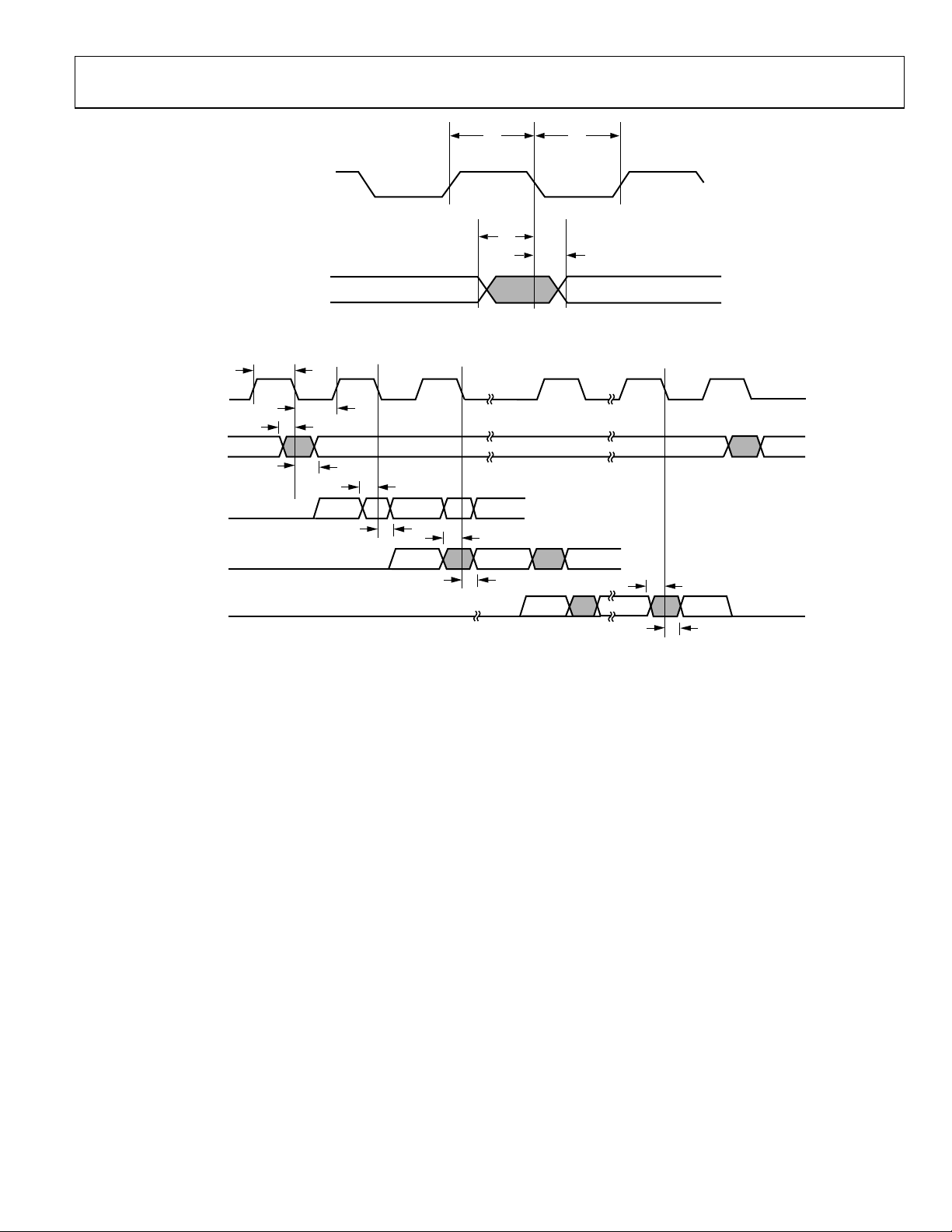
09580-004
t
9
LLC
P0 TO P47, HS ,
VS/FIELD/ALSB, DE
t
11
t
12
t
10
SCLK
LRCLK
I2Sx
LEFT-JUSTIFIED
MODE
I2Sx
RIGHT-JUSTIFIED
MODE
I2Sx
I
2
S MODE
MSB MSB – 1
t
15
t
16
t
17
t
19
t
20
t
18
MSB
MSB – 1
LSBMSB
t
19
t
20
t
19
t
20
NOTES
1. THE LRCLK SIGNAL IS AV AILABLE O N THE AP5 PIN.
2. I2Sx SI GNALS (WHERE x = 0, 1, 2, OR 3) ARE AV AILABLE
ON THE FOLLOW ING PINS: AP 1, AP2, AP3, AND AP 4.
09580-005
Figure 4. Pixel Port and Control SDR Output Timing
Figure 5. I
2
S Timing
Rev. B | Page 7 of 24
ADV7619 Data Sheet
PVDD to GND
2.2 V
ABSOLUTE MAXIMUM RATINGS
Table 4.
Parameter Rating
DVDD to GND 2.2 V
DVDDIO to GND 4.0 V
CVDD to GND 2.2 V
TVDD to GND 4.0 V
Digital Inputs to GND GND − 0.3 V to DVDDIO + 0.3 V
5 V Tolerant Digital Inputs
to GND
1
5.3 V
Digital Outputs to GND GND − 0.3 V to DVDDIO + 0.3 V
XTALP, XTALN −0.3 V to PVDD + 0.3 V
SCL, SDA Data Pins to
DVDDIO − 0.3 V to DVDDIO + 3.6 V
DVDDIO
Maximum Junction
Temperature (T
J MAX
)
125°C
Storage Temperature Range −60°C to +150°C
Infrared Reflow Soldering
260°
(20 sec)
1
The following inputs are 3.3 V inputs but are 5 V tolerant: DDCA_SCL,
DDCA_SDA, DDCB_SCL, and DDCB_SDA.
Stresses above those listed under Absolute Maximum Ratings
may cause permanent damage to the device. This is a stress
rating only; functional operation of the device at these or any
other conditions above those indicated in the operational
section of this specification is not implied. Exposure to absolute
maximum rating conditions for extended periods may affect
device reliability.
PACKAGE THERMAL PERFORMANCE
To reduce power consumption when using the ADV7619, the
user is advised to turn off the unused sections of the part.
Due to PCB metal variation and, therefore, variation in PCB
heat conductivity, the value of θ
may differ for various PCBs.
JA
The most efficient measurement solution is obtained using the
package surface temperature to estimate the die temperature
because this solution eliminates the variance associated with
the θ
value.
JA
The maximum junction temperature (T
) of 125°C must not
J MAX
be exceeded. The following equation calculates the junction
temperature using the measured package surface temperature
and applies only when no heat sink is used on the device under
test (DUT):
T
= TS + (ΨJT × W
J
TOTAL
)
where:
T
is the package surface temperature (°C).
S
= 0.22°C/W for the 128-lead TQFP_EP.
Ψ
JT
= ((PVDD × I
W
TOTA L
(CVDD × I
) + (DVDD × I
CVDD
) + (0.2 × TVDD × I
PVDD
) + (DVDDIO × I
DVDD
TVDD
) +
DVDDIO
))
where 0.2 is 20% of the TVDD power that is dissipated on the
part itself.
ESD CAUTION
Rev. B | Page 8 of 24

Data Sheet ADV7619
A_A/INT2
PIN CONFIGURATION AND FUNCTION DESCRIPTIONS
CVDD
RXA_C–
RXA_C+
TVDD
RXA_0–
RXA_0+
TVDD
RXA_1–
RXA_1+
TVDD
RXA_2–
RXA_2+
CVDD
TEST1
DVDD
TEST2
CVDD
RXB_C–
RXB_C+
TVDD
RXB_0–
RXB_0+
TVDD
RXB_1–
RXB_1+
TVDD
RXB_2–
RXB_2+
CVDD
GND
GND
GND
NC
127
128
1
2
3
4
5
6
7
8
9
10
11
12
13
14
15
16
17
18
19
20
21
22
23
24
25
26
27
28
29
30
31
32
PIN 1
NC
RXA_5V
126
125
HP
DDCA_SDA
124
DDCA_SCL
123
RXB_5V
122
HPA_B
121
120
DDCB_SDA
DDCB_SCL
DVDD
CEC
XTALN
119
118
117
116
CS
PVDD
XTALP
114
113
115
ADV7619
TOP VIEW
(Not to S cale)
RESET
112
INT1
SCL
SDA
DVDD
AP5
SCLK/INT2
106
105
104
AP4
AP2
AP3
AP1
AP099NC98NC97NC
102
100
101
103
96
NC
95
VS/FIELD/ALSB
94
HS
93
DE
92
DVDDIO
91
P0
90
P1
89
P2
88
P3
87
P4
86
P5
85
P6
84
P7
83
P8
82
P9
81
P10
80
P11
79
DVDD
78
P12
77
DVDDIO
76
P13
75
P14
74
P15
73
P16
72
P17
71
P18
70
P19
69
P20
68
P21
67
P22
66
P23
65
DVDDIO
MCLK/INT2
108
109
110
111
107
41
33
35
34
NC
P4736P4637P4538P4439P43
DVDD
NOTES
1. NC = NO CONNE C T. DO NOT CONNECT TO THIS PIN.
2. CONNECT THE EXPOSED PAD (PIN 0) ON THE BOTTOM
OF THEPACKAGE TO GROUND.
40
P4242P4143P4044P3945P3846P3747P3648P3549P3450P33
DVDDIO
53
51
52
P32
DVDD
DVDDIO
Figure 6. Pin Configuration
Rev. B | Page 9 of 24
54
P3155P3056P2957P2858P2759P2660P2561P24
62
LLC
63
DVDD64DVDD
09580-008

ADV7619 Data Sheet
4
RXA_C+
HDMI input
Digital Input Clock True of Port A in the HDMI Interface.
9
RXA_1−
HDMI input
Digital Input Channel 1 Complement of Port A in the HDMI Interface.
15
GND
Ground
Ground.
26
RXB_1−
HDMI input
Digital Input Channel 1 Complement of Port B in the HDMI Interface.
37
P45
Digital video output
Video Pixel Output Port.
48
P35
Digital video output
Video Pixel Output Port.
Table 5. Pin Function Descriptions
Pin No. Mnemonic Type Description
0 GND Ground Ground. Connect the exposed pad (Pin 0) on the bottom of the package to ground.
1 GND Ground Ground.
2 CVDD Power HDMI Analog Block Supply Voltage (1.8 V).
3 RXA_C− HDMI input Digital Input Clock Complement of Port A in the HDMI Interface.
5 TVDD Power Terminator Supply Voltage (3.3 V).
6 RXA_0− HDMI input Digital Input Channel 0 Complement of Port A in the HDMI Interface.
7 RXA_0+ HDMI input Digital Input Channel 0 True of Port A in the HDMI Interface.
8 TVDD Power Terminator Supply Voltage (3.3 V).
10 RXA_1+ HDMI input Digital Input Channel 1 True of Port A in the HDMI Interface.
11 TVDD Power Terminator Supply Voltage (3.3 V).
12 RXA_2− HDMI input Digital Input Channel 2 Complement of Port A in the HDMI Interface.
13 RXA_2+ HDMI input Digital Input Channel 2 True of Port A in the HDMI Interface.
14 CVDD Power HDMI Analog Block Supply Voltage (1.8 V ).
16 TEST1 Test This pin must be left floating.
17 DVDD Power Digital Core Supply Voltage (1.8 V).
18 TEST2 Test This pin must be left floating.
19 CVDD Power HDMI Analog Block Supply Voltage (1.8 V).
20 RXB_C− HDMI input Digital Input Clock Complement of Port B in the HDMI Interface.
21 RXB_C+ HDMI input Digital Input Clock True of Port B in the HDMI Interface.
22 TVDD Power Terminator Supply Voltage (3.3 V).
23 RXB_0− HDMI input Digital Input Channel 0 Complement of Port B in the HDMI Interface.
24 RXB_0+ HDMI input Digital Input Channel 0 True of Port B in the HDMI Interface.
25 TVDD Power Terminator Supply Voltage (3.3 V).
27 RXB_1+ HDMI input Digital Input Channel 1 True of Port B in the HDMI Interface.
28 TVDD Power Terminator Supply Voltage (3.3 V).
29 RXB_2− HDMI input Digital Input Channel 2 Complement of Port B in the HDMI Interface.
30 RXB_2+ HDMI input Digital Input Channel 2 True of Port B in the HDMI Interface.
31 CVDD Power HDMI Analog Block Supply Voltage (1.8 V).
32 GND Ground Ground.
33 NC No connect No Connect. Do not connect to this pin.
34 DVDD Power Digital Core Supply Voltage (1.8 V).
35 P47 Digital video output Video Pixel Output Port.
36 P46 Digital video output Video Pixel Output Port.
38 P44 Digital video output Video Pixel Output Port.
39 P43 Digital video output Video Pixel Output Port.
40 DVDDIO Power Digital I/O Supply Voltage (3.3 V).
41 P42 Digital video output Video Pixel Output Port.
42 P41 Digital video output Video Pixel Output Port.
43 P40 Digital video output Video Pixel Output Port.
44 P39 Digital video output Video Pixel Output Port.
45 P38 Digital video output Video Pixel Output Port.
46 P37 Digital video output Video Pixel Output Port.
47 P36 Digital video output Video Pixel Output Port.
49 P34 Digital video output Video Pixel Output Port.
50 P33 Digital video output Video Pixel Output Port.
51 P32 Digital video output Video Pixel Output Port.
Rev. B | Page 10 of 24

Data Sheet ADV7619
56
P29
Digital video output
Video Pixel Output Port.
62
LLC
Digital video output
Pixel Output Clock for the Pixel Data. The range is from 13.5 MHz to 170 MHz.
73
P16
Digital video output
Video Pixel Output Port.
79
DVDD
Power
Digital Core Supply Voltage (1.8 V).
90
P1
Digital video output
Video Pixel Output Port.
100
AP0
Miscellaneous
Pin No. Mnemonic Type Description
52 DVDDIO Power Digital I/O Supply Voltage (3.3 V).
53 DVDD Power Digital Core Supply Voltage (1.8 V).
54 P31 Digital video output Video Pixel Output Port.
55 P30 Digital video output Video Pixel Output Port.
57 P28 Digital video output Video Pixel Output Port.
58 P27 Digital video output Video Pixel Output Port.
59 P26 Digital video output Video Pixel Output Port.
60 P25 Digital video output Video Pixel Output Port.
61 P24 Digital video output Video Pixel Output Port.
63 DVDD Power Digital Core Supply Voltage (1.8 V).
64 DVDD Power Digital Core Supply Voltage (1.8 V).
65 DVDDIO Power Digital I/O Supply Voltage (3.3 V).
66 P23 Digital video output Video Pixel Output Port.
67 P22 Digital video output Video Pixel Output Port.
68 P21 Digital video output Video Pixel Output Port.
69 P20 Digital video output Video Pixel Output Port.
70 P19 Digital video output Video Pixel Output Port.
71 P18 Digital video output Video Pixel Output Port.
72 P17 Digital video output Video Pixel Output Port.
74 P15 Digital video output Video Pixel Output Port.
75 P14 Digital video output Video Pixel Output Port.
76 P13 Digital video output Video Pixel Output Port.
77 DVDDIO Power Digital I/O Supply Voltage (3.3 V).
78 P12 Digital video output Video Pixel Output Port.
80 P11 Digital video output Video Pixel Output Port.
81 P10 Digital video output Video Pixel Output Port.
82 P9 Digital video output Video Pixel Output Port.
83 P8 Digital video output Video Pixel Output Port.
84 P7 Digital video output Video Pixel Output Port.
85 P6 Digital video output Video Pixel Output Port.
86 P5 Digital video output Video Pixel Output Port.
87 P4 Digital video output Video Pixel Output Port.
88 P3 Digital video output Video Pixel Output Port.
89 P2 Digital video output Video Pixel Output Port.
91 P0 Digital video output Video Pixel Output Port.
92 DVDDIO Power Digital I/O Supply Voltage (3.3 V).
93 DE Miscellaneous digital Data Enable. The DE signal indicates active pixel data.
94 HS Digital video output Horizontal Synchronization Output Signal.
95 VS/FIELD/ALSB Digital video output
VS is a vertical synchronization output signal. FIELD is a field synchronization output
signal in all interlaced video modes. ALSB allows selection of the I
96 NC No connect No Connect. Do not connect to this pin.
97 NC No connect No Connect. Do not connect to this pin.
98 NC No connect No Connect. Do not connect to this pin.
99 NC No connect No Connect. Do not connect to this pin.
Audio Output Pin. This pin can be configured to output S/PDIF digital audio, high bit
rate (HBR), or Direct Stream Digital® (DSD®).
101 AP1 Miscellaneous
Audio Output Pin/TDM I
2
S Output. This pin can be configured to output S/PDIF digital
audio, high bit rate (HBR), Direct Stream Digital (DSD).
2
C address.
Rev. B | Page 11 of 24

ADV7619 Data Sheet
123
DDCA_SCL
HDMI input
HDCP Slave Serial Clock Port A. DDCA_SCL is a 3.3 V input that is 5 V tolerant.
128
NC
No connect
No Connect. Do not connect to this pin.
Pin No. Mnemonic Type Description
102 AP2 Miscellaneous
103 AP3 Miscellaneous
104 AP4 Miscellaneous
105 SCLK/INT2 Miscellaneous digital
106 AP5 Miscellaneous
107 MCLK/INT2 Miscellaneous digital
108 DVDD Power Digital Core Supply Voltage (1.8 V ).
109 SDA Miscellaneous digital I2C Port Serial Data Input/Output Pin. SDA is the data line for the control port.
110 SCL Miscellaneous digital I2C Port Serial Clock Input. SCL is the clock line for the control port.
111 INT1 Miscellaneous digital
112
113
RESET
CS
Miscellaneous digital
Miscellaneous digital
114 PVDD Power PLL Supply Voltage (1.8 V).
115 XTALP Miscellaneous
116 XTALN Miscellaneous Crystal Input. Input pin for 28.63636 MHz crystal.
117 DVDD Power Digital Core Supply Voltage (1.8 V).
118 CEC Digital input/output Consumer Electronics Control Channel.
119 DDCB_SCL HDMI input HDCP Slave Serial Clock Port B. DDCB_SCL is a 3.3 V input that is 5 V tolerant.
120 DDCB_SDA HDMI input HDCP Slave Serial Data Port B. DDCB_SDA is a 3.3 V input that is 5 V tolerant.
121 HPA_B Miscellaneous digital Hot Plug Assert Signal Output for HDMI Port B.
122 RXB_5V HDMI input 5 V Detect Pin for Port B in the HDMI Interface.
Audio Output Pin. This pin can be configured to output S/PDIF digital audio, high bit
rate (HBR), Direct Stream Digital (DSD), or I
2
S.
Audio Output Pin. This pin can be configured to output S/PDIF digital audio, high bit
rate (HBR), Direct Stream Digital (DSD), or I2S.
Audio Output Pin. This pin can be configured to output S/PDIF digital audio, high bit
rate (HBR), Direct Stream Digital (DSD), or I
2
S.
Serial Clock/Interrupt 2. This dual-function pin can be configured to output the audio
serial clock or an Interrupt 2 signal.
Audio Output Pin. This pin can be configured to output S/PDIF digital audio, high bit
rate (HBR), or Direct Stream Digital (DSD). Pin AP5 is typically used to provide the
LRCLK for I
2
S modes.
Master Clock/Interrupt 2. This dual-function pin can be configured to output the audio
master clock or an Interrupt 2 signal.
Interrupt. This pin can be active low or active high. When status bits change, this pin is
triggered. The events that trigger an interrupt are user configurable.
System Reset Input. Active low. A minimum low reset pulse width of 5 ms is required
to reset the ADV7619 circuitry.
Chip Select. This pin has an internal pull-down. Pulling this line up causes I2C state
machine to ignore I
2
C transmission.
Input Pin for 28.63636 MHz Crystal or External 1.8 V, 28.63636 MHz Clock Oscillator
Source to Clock the ADV7619.
124 DDCA_SDA HDMI input HDCP Slave Serial Data Port A. DDCA_SDA is a 3.3 V input that is 5 V tolerant.
125 HPA_A/INT2 Miscellaneous digital
Hot Plug Assert/Interrupt 2. This dual-function pin can be configured to output the
Hot Plug assert signal for HDMI Port A or an Interrupt 2 signal.
126 RXA_5V HDMI input 5 V Detect Pin for Port A in the HDMI Interface.
127 NC No connect No Connect. Do not connect to this pin.
Rev. B | Page 12 of 24

Data Sheet ADV7619
09580-007
3.3V SUPPLIES
POWER SUPPLY (V)
3.3V SUPPLIES
POWER-UP
1.8V SUPPLIES
POWER-UP
3.3V
1.8V
1.8V SUPPLIES
POWER SUPPLY RECOMMENDATIONS
POWER-UP SEQUENCE
The recommended power-up sequence for the ADV7619 is to
power up the 3.3 V supplies first, followed by the 1.8 V supplies.
should be held low while the supplies are powered up.
RESET
Alternatively, the ADV7619 can be powered up by asserting all
supplies simultaneously. In this case, care must be taken while
the supplies are being established to ensure that a lower rated
supply does not go above a higher rated supply level.
POWER-DOWN SEQUENCE
The ADV7619 supplies can be deasserted simultaneously as long
as a higher rated supply does not go below a lower rated supply.
CURRENT RATING REQUIREMENTS FOR POWER SUPPLY DESIGN
Tabl e 6 shows the current rating requirements for power supply
design.
Table 6. Current Rating Requirements for Power Supply Design
Parameter Current Rating (mA)
I
400
DVDD
I
300
DVDDIO
I
50
PVDD
I
120
TVDD
I
250
CVDD
Figure 7. Recommended Power-Up Sequence
Rev. B | Page 13 of 24

ADV7619 Data Sheet
FUNCTIONAL OVERVIEW
HDMI RECEIVER
The HDMI receiver supports all mandatory and many optional
3D video formats defined in the HDMI 1.4a specification, HDTV
formats up to 2160p, and all display resolutions up to 4k × 2k
(3840 × 2160 at 30 Hz).
With the inclusion of HDCP, displays can now receive encrypted
video content. The HDMI interface of the ADV7619 allows for
authentication of a video receiver, decryption of encoded data at
the receiver, and renewability of that authentication during transmission, as specified by the HDCP 1.4 specification.
The HDMI-compatible receiver on the ADV7619 allows active
equalization of the HDMI data signals. This equalization compensates for the high frequency losses inherent in HDMI and DVI
cabling, especially at longer cable lengths and higher frequencies.
The HDMI-compatible receiver is capable of equalizing for cable
lengths up to 30 meters to achieve robust receiver performance.
The ADV7619 also supports TERC4 error detection, which is
used for detection of corrupted HDMI packets following a cable
disconnect.
The HDMI receiver offers advanced audio functionality. The
receiver contains an audio mute controller that can detect a variety
of conditions that may result in audible extraneous noise in the
audio output. Upon detection of these conditions, the audio signal
can be ramped down or muted to prevent audio clicks or pops.
The HDMI receiver supports the reception of all types of audio
data described in the HDMI specifications, including
• LPCM (uncompressed audio)
• IEC 61937 (compressed audio)
• DSD audio (1-bit audio)
• HBR audio (high bit rate compressed audio)
Xpressview fast switching can be implemented with full HDCP
authentication available on the background port. Synchronization measurement and status information are available for all
HDMI inputs. HDMI receiver features include
• 2:1 multiplexed HDMI receiver
• 3D format support
• 297 MHz HDMI receiver
• Support for 4k × 2k resolutions
• Integrated equalizer for cable lengths up to 30 meters
• High-bandwidth Digital Content Protection (HDCP 1.4)
(on background ports, also)
• Internal HDCP keys
• 36-/30-bit Deep Color support (resolutions up to 1080p)
• Audio sample, HBR, DSD packet support
• Repeater support
• Internal EDID RAM
• Hot Plug assert output pin for each HDMI port
Rev. B | Page 14 of 24
• CEC controller
COMPONENT PROCESSOR (CP)
The ADV7619 has two any-to-any, 3 × 3 color space conversion
(CSC) matrices. The first CSC block is placed in front of the CP
section. The second CSC block is placed at the back of the CP
section. Each CSC enables YPrPb-to-RGB and RGB-to-YCrCb
conversions. Many other standards of color space can be implemented using the color space converters.
The CP block is available only for video signals with resolution
up to 1080p Deep Color (pixel rates up to 170 MHz). For resolutions higher than 1080p, the video signal bypasses the CP block
and is routed directly to the pixel bus output as two 24-bit (4:4:4)
buses running at up to 150 MHz.
CP features include
• Support for 525i, 625i, 525p, 625p, 720p, 1080i, 1080p,
and many other HDTV formats
• Manual adjustments including gain (contrast), offset
(brightness), hue, and saturation
• Free-run output mode that provides stable timing when
no video input is present
• 170 MHz conversion rate, which supports RGB input
resolutions up to 1600 × 1200 at 60 Hz
• Standard identification enabled by STDI block
• RGB that can be color space converted to YCrCb and
de
cimated to a 4:2:2 format for video-centric, back-end
IC interfacing
• Data enable (DE) output signal supplied for direct
connection to HDMI/DVI transmitter
OTHER FEATURES
The ADV7619 has HS, VS, FIELD, and DE output signals with
programmable position, polarity, and width.
The ADV7619 has two programmable interrupt request output
pins: INT1 and INT2 (INT2 is accessible via one of the following
pins: MCLK/INT2, SCLK/INT2, or HPA_A/INT2). The ADV7619
also features a low power power-down mode.
The main I
after a reset, the I
can be changed to 0x9A by pulling up the VS/FIELD/ALSB pin
and issuing the I
mation, see the Register Access and Serial Ports Description
section in the UG-237.
The ADV7619 is provided in a 128-lead, 14 mm × 14 mm,
RoHS-compliant TQFP_EP package and is specified over the
0°C to 70°C temperature range.
2
C address can be set to 0x98 or 0x9A. On power-up or
2
C address is set to 0x98 by default. The address
2
C command SAMPLE_ALSB. For more infor-

Data Sheet ADV7619
PIXEL INPUT/OUTPUT FORMATTING
The output section of the ADV7619 is highly flexible. The pixel
output bus can support up to 36-bit 4:4:4 YCrCb or 36-bit 4:4:4
RGB. For resolutions higher than 1080p, the pixel output bus
supports two 24-bit 4:4:4 RGB/YCrCb.
Part supports SDR (single data rate) and double data rate
(DDR) outputs. SDR is supported up to 170 MHz LLC
frequency (UXGA, 1080p60 for any OP_FORMAT_SEL or
up to 300 MHz HDMI signals output on two 24-bit parallel
video sub buses OP_FORMAT_SEL = 0x94, 0x95, 0x96, or
0x54; refer to Tab le 12). DDR can be supported with LLC clock
frequency up to 50 MHz (video modes with original pixel clock
lower than 100 MHz, such as 1080i60). In SDR mode, 16-/20-/
24-bit 4:2:2 or 24-/30-/36-bit 4:4:4 output is possible. In DDR
mode, the pixel output port can be configured for 4:2:2 YCrCb
or 4:4:4 RGB for data rates up to 27 MHz.
Bus rotation is supported.
Tabl e 7 through Tab l e 12 provide the different output formats
that are supported. All output modes are controlled via I
For resolutions higher than 1080p, the video signals are routed
directly to the pixel bus output as two 24-bit (4:4:4) buses running
at up to 150 MHz. In this mode, the output data format is the
same as the input format.
2
C.
PIXEL DATA OUTPUT MODE FEATURES
For resolutions up to 1080p Deep Color, the output pixel port
features include the following:
• SDR 8-/10-/12-bit ITU-R BT.656 4:2:2 YCrCb with embed-
ded time codes and/or HS, VS, and FIELD output signals
• SDR 16-/20-/24-bit 4:2:2 YCrCb with embedded time codes
and/or HS and VS/FIELD pin timing
• SDR 24-/30-/36-bit 4:4:4 YCrCb/RGB with embedded time
codes and/or HS and VS/FIELD pin timing
• DDR 8-/10-/12-bit 4:2:2 YCrCb for data rates up to 27 MHz
• DDR 12-/24-/30-/36-bit 4:4:4 RGB for data rates up to
27 MHz
For resolutions greater than 1080p Deep Color (direct passthrough of video signal), the output pixel port features include
the following:
• 8-bit 4:4:4 RGB/YCrCb for resolutions up to 2160p
• 12-bit 4:2:2 RGB/YCrCb for resolutions up to 2160p
Rev. B | Page 15 of 24

ADV7619 Data Sheet
P32
High-Z
High-Z
High-Z
High-Z
Y0, Cb0, Cr0
P20
Y4, Cb4, Cr4
Y6, Cb6, Cr6
Y8, Cb8, Cr8
Y8, Cb8, Cr8
Y8, Cb8, Cr8
P19
Y3, Cb3, Cr3
Y5, Cb5, Cr5
Y7, Cb7, Cr7
Y7, Cb7, Cr7
Y7, Cb7, Cr7
P1
High-Z
High-Z
High-Z
High-Z
High-Z
Table 7. SDR 4:2:2 Output Modes (8-/10-/12-Bit)1
SDR 4:2:2—OP_FORMAT_SEL[7:0] =
0x00 0x01 0x02 0x06 0x0A
8-Bit SDR
Pixel Output
P47 High-Z High-Z High-Z High-Z High-Z
P46 High-Z High-Z High-Z High-Z High-Z
P45 High-Z High-Z High-Z High-Z High-Z
P44 High-Z High-Z High-Z High-Z High-Z
P43 High-Z High-Z High-Z High-Z High-Z
P42 High-Z High-Z High-Z High-Z High-Z
P41 High-Z High-Z High-Z High-Z High-Z
P40 High-Z High-Z High-Z High-Z High-Z
P39 High-Z High-Z High-Z High-Z High-Z
P38 High-Z High-Z High-Z High-Z High-Z
P37 High-Z High-Z High-Z High-Z High-Z
P36 High-Z High-Z High-Z High-Z High-Z
P35 High-Z High-Z High-Z High-Z Y3, Cb3, Cr3
P34 High-Z High-Z High-Z High-Z Y2, Cb2, Cr2
P33 High-Z High-Z High-Z High-Z Y1, Cb1, Cr1
P31 High-Z High-Z High-Z High-Z High-Z
P30 High-Z High-Z High-Z High-Z High-Z
P29 High-Z High-Z High-Z Y1, Cb1, Cr1 High-Z
P28 High-Z High-Z High-Z Y0, Cb0, Cr0 High-Z
P27 High-Z High-Z High-Z High-Z High-Z
P26 High-Z High-Z High-Z High-Z High-Z
P25 High-Z High-Z High-Z High-Z High-Z
P24 High-Z High-Z High-Z High-Z High-Z
P23 Y7, Cb7, Cr7 Y9, Cb9, Cr9 Y11, Cb11, Cr11 Y11, Cb11, Cr11 Y11, Cb11, Cr11
P22 Y6, Cb6, Cr6 Y8, Cb8, Cr8 Y10, Cb10, Cr10 Y10, Cb10, Cr10 Y10, Cb10, Cr10
P21 Y5, Cb5, Cr5 Y7, Cb7, Cr7 Y9, Cb9, Cr9 Y9, Cb9, Cr9 Y9, Cb9, Cr9
ITU-R BT.656
Mode 0
10-Bit SDR
ITU-R BT.656
Mode 0
12-Bit SDR
ITU-R BT.656
Mode 0
12-Bit SDR
ITU-R BT.656
Mode 1
12-Bit SDR
ITU-R BT.656
Mode 2
P18 Y2, Cb2, Cr2 Y4, Cb4, Cr4 Y6, Cb6, Cr6 Y6, Cb6, Cr6 Y6, Cb6, Cr6
P17 Y1, Cb1, Cr1 Y3, Cb3, Cr3 Y5, Cb5, Cr5 Y5, Cb5, Cr5 Y5, Cb5, Cr5
P16 Y0, Cb0, Cr0 Y2, Cb2, Cr2 Y4, Cb4, Cr4 Y4, Cb4, Cr4 Y4, Cb4, Cr4
P15 High-Z Y1, Cb1, Cr1 Y3, Cb3, Cr3 Y3, Cb3, Cr3 High-Z
P14 High-Z Y0, Cb0, Cr0 Y2, Cb2, Cr2 Y2, Cb2, Cr2 High-Z
P13 High-Z High-Z Y1, Cb1, Cr1 High-Z High-Z
P12 High-Z High-Z Y0, Cb0, Cr0 High-Z High-Z
P11 High-Z High-Z High-Z High-Z High-Z
P10 High-Z High-Z High-Z High-Z High-Z
P9 High-Z High-Z High-Z High-Z High-Z
P8 High-Z High-Z High-Z High-Z High-Z
P7 High-Z High-Z High-Z High-Z High-Z
P6 High-Z High-Z High-Z High-Z High-Z
P5 High-Z High-Z High-Z High-Z High-Z
P4 High-Z High-Z High-Z High-Z High-Z
P3 High-Z High-Z High-Z High-Z High-Z
P2 High-Z High-Z High-Z High-Z High-Z
P0 High-Z High-Z High-Z High-Z High-Z
1
Modes require additional writes to IO map Register 0x19 (Bits[7:6] should be set to 2'b11) and IO map Register 0x33 (Bit[6] should be set to 1).
Rev. B | Page 16 of 24

Data Sheet ADV7619
P45
High-Z
High-Z
High-Z
High-Z
High-Z
P39
High-Z
High-Z
High-Z
High-Z
High-Z
P28
High-Z
High-Z
High-Z
Y0
Cb0, Cr0
P17
Y1
Y3
Y5
Y5
Y5
P6
Cb2, Cr2
Cb4, Cr4
Cb6, Cr6
Cb6, Cr6
Cb6, Cr6
Table 8. SDR 4:2:2 Output Modes (16-/20-/24-Bit)
SDR 4:2:2—OP_FORMAT_SEL[7:0] =
0x80 0x81 0x82 0x86 0x8A
16-Bit SDR
ITU-R BT.656
Pixel Output
Mode 0
P47 High-Z High-Z High-Z High-Z High-Z
P46 High-Z High-Z High-Z High-Z High-Z
P44 High-Z High-Z High-Z High-Z High-Z
P43 High-Z High-Z High-Z High-Z High-Z
P42 High-Z High-Z High-Z High-Z High-Z
P41 High-Z High-Z High-Z High-Z High-Z
P40 High-Z High-Z High-Z High-Z High-Z
P38 High-Z High-Z High-Z High-Z High-Z
P37 High-Z High-Z High-Z High-Z High-Z
P36 High-Z High-Z High-Z High-Z High-Z
P35 High-Z High-Z High-Z High-Z Y3
P34 High-Z High-Z High-Z High-Z Y2
P33 High-Z High-Z High-Z Cb1, Cr1 Y1
P32 High-Z High-Z High-Z Cb0, Cr0 Y0
P31 High-Z High-Z High-Z High-Z Cb3, Cr3
P30 High-Z High-Z High-Z High-Z Cb2, Cr2
P29 High-Z High-Z High-Z Y1 Cb1, Cr1
20-Bit SDR
ITU-R BT.656
Mode 0
24-Bit SDR
ITU-R BT.656
Mode 0
24-Bit SDR
ITU-R BT.656
Mode 1
24-Bit SDR
ITU-R BT.656
Mode 2
P27 High-Z High-Z High-Z High-Z High-Z
P26 High-Z High-Z High-Z High-Z High-Z
P25 High-Z High-Z High-Z High-Z High-Z
P24 High-Z High-Z High-Z High-Z High-Z
P23 Y7 Y9 Y11 Y11 Y11
P22 Y6 Y8 Y10 Y10 Y10
P21 Y5 Y7 Y9 Y9 Y9
P20 Y4 Y6 Y8 Y8 Y8
P19 Y3 Y5 Y7 Y7 Y7
P18 Y2 Y4 Y6 Y6 Y6
P16 Y0 Y2 Y4 Y4 Y4
P15 High-Z Y1 Y3 Y3 High-Z
P14 High-Z Y0 Y2 Y2 High-Z
P13 High-Z High-Z Y1 High-Z High-Z
P12 High-Z High-Z Y0 High-Z High-Z
P11 Cb7, Cr7 Cb9, Cr9 Cb11, Cr11 Cb11, Cr11 Cb11, Cr11
P10 Cb6, Cr6 Cb8, Cr8 Cb10, Cr10 Cb10, Cr10 Cb10, Cr10
P9 Cb5, Cr5 Cb7, Cr7 Cb9, Cr9 Cb9, Cr9 Cb9, Cr9
P8 Cb4, Cr4 Cb6, Cr6 Cb8, Cr8 Cb8, Cr8 Cb8, Cr8
P7 Cb3, Cr3 Cb5, Cr5 Cb7, Cr7 Cb7, Cr7 Cb7, Cr7
P5 Cb1, Cr1 Cb3, Cr3 Cb5, Cr5 Cb5, Cr5 Cb5, Cr5
P4 Cb0, Cr0 Cb2, Cr2 Cb4, Cr4 Cb4, Cr4 Cb4, Cr4
P3 High-Z Cb1, Cr1 Cb3, Cr3 Cb3, Cr3 High-Z
P2 High-Z Cb0, Cr0 Cb2, Cr2 Cb2, Cr2 High-Z
P1 High-Z High-Z Cb1, Cr1 High-Z High-Z
P0 High-Z High-Z Cb0, Cr0 High-Z High-Z
Rev. B | Page 17 of 24

ADV7619 Data Sheet
P43
High-Z
High-Z
High-Z
High-Z
P32
R4
R6
R8
R6
P21
G5
G7
G9
G3
P15
High-Z
G1
G3
B9
P10
B6
B8
B10
B6
P4
B0
B2
B4
B0
Table 9. SDR 4:4:4 Output Modes
SDR 4:4:4—OP_FORMAT_SEL[7:0] =
0x40 0x41 0x42 0x46
24-Bit SDR
Pixel Output
P47 High-Z High-Z High-Z High-Z
P46 High-Z High-Z High-Z High-Z
P45 High-Z High-Z High-Z High-Z
P44 High-Z High-Z High-Z High-Z
P42 High-Z High-Z High-Z High-Z
P41 High-Z High-Z High-Z High-Z
P40 High-Z High-Z High-Z High-Z
P39 High-Z High-Z High-Z High-Z
P38 High-Z High-Z High-Z High-Z
P37 High-Z High-Z High-Z High-Z
P36 High-Z High-Z High-Z High-Z
P35 R7 R9 R11 R9
P34 R6 R8 R10 R8
P33 R5 R7 R9 R7
P31 R3 R5 R7 R5
P30 R2 R4 R6 R4
P29 R1 R3 R5 R3
P28 R0 R2 R4 R2
P27 High-Z R1 R3 R1
P26 High-Z R0 R2 R0
P25 High-Z High-Z R1 G7
P24 High-Z High-Z R0 G6
P23 G7 G9 G11 G5
P22 G6 G8 G10 G4
Mode 0
30-Bit SDR
Mode 0
36-Bit SDR
Mode 0
36-Bit SDR
Mode 1
P20 G4 G6 G8 G2
P19 G3 G5 G7 G1
P18 G2 G4 G6 G0
P17 G1 G3 G5 B11
P16 G0 G2 G4 B10
P14 High-Z G0 G2 B8
P13 High-Z High-Z G1 G11
P12 High-Z High-Z G0 G10
P11 B7 B9 B11 B7
P9 B5 B7 B9 B5
P8 B4 B6 B8 B4
P7 B3 B5 B7 B3
P6 B2 B4 B6 B2
P5 B1 B3 B5 B1
P3 High-Z B1 B3 R11
P2 High-Z B0 B2 R10
P1 High-Z High-Z B1 G9
P0 High-Z High-Z B0 G8
Rev. B | Page 18 of 24

Data Sheet ADV7619
P42
High-Z
High-Z
High-Z
High-Z
High-Z
High-Z
P31
High-Z
High-Z
High-Z
High-Z
High-Z
High-Z
P20
Cb4, Cr4
Y4
Cb6, Cr6
Y6
Cb8, Cr8
Y8
P9
High-Z
High-Z
High-Z
High-Z
High-Z
High-Z
P3
High-Z
High-Z
High-Z
High-Z
High-Z
High-Z
Table 10. DDR 4:2:2 Output Modes
DDR 4:2:2 Mode (Clock/2)—OP_FORMAT_SEL[7:0] =
0x20 0x21 0x22
8-Bit DDR
ITU-R BT.656, Mode 0
Pixel Output
P47 High-Z High-Z High-Z High-Z High-Z High-Z
P46 High-Z High-Z High-Z High-Z High-Z High-Z
P45 High-Z High-Z High-Z High-Z High-Z High-Z
P44 High-Z High-Z High-Z High-Z High-Z High-Z
P43 High-Z High-Z High-Z High-Z High-Z High-Z
P41 High-Z High-Z High-Z High-Z High-Z High-Z
P40 High-Z High-Z High-Z High-Z High-Z High-Z
P39 High-Z High-Z High-Z High-Z High-Z High-Z
P38 High-Z High-Z High-Z High-Z High-Z High-Z
P37 High-Z High-Z High-Z High-Z High-Z High-Z
P36 High-Z High-Z High-Z High-Z High-Z High-Z
P35 High-Z High-Z High-Z High-Z High-Z High-Z
P34 High-Z High-Z High-Z High-Z High-Z High-Z
P33 High-Z High-Z High-Z High-Z High-Z High-Z
P32 High-Z High-Z High-Z High-Z High-Z High-Z
Clock Rise Clock Fall Clock Rise Clock Fall Clock Rise Clock Fall
10-Bit DDR
ITU-R BT.656, Mode 0
12-Bit DDR
ITU-R BT.656, Mode 0
P30 High-Z High-Z High-Z High-Z High-Z High-Z
P29 High-Z High-Z High-Z High-Z High-Z High-Z
P28 High-Z High-Z High-Z High-Z High-Z High-Z
P27 High-Z High-Z High-Z High-Z High-Z High-Z
P26 High-Z High-Z High-Z High-Z High-Z High-Z
P25 High-Z High-Z High-Z High-Z High-Z High-Z
P24 High-Z High-Z High-Z High-Z High-Z High-Z
P23 Cb7, Cr7 Y7 Cb9, Cr9 Y9 Cb11, Cr11 Y11
P22 Cb6, Cr6 Y6 Cb8, Cr8 Y8 Cb10, Cr10 Y10
P21 Cb5, Cr5 Y5 Cb7, Cr7 Y7 Cb9, Cr9 Y9
P19 Cb3, Cr3 Y3 Cb5, Cr5 Y5 Cb7, Cr7 Y7
P18 Cb2, Cr2 Y2 Cb4, Cr4 Y4 Cb6, Cr6 Y6
P17 Cb1, Cr1 Y1 Cb3, Cr3 Y3 Cb5, Cr5 Y5
P16 Cb0, Cr0 Y0 Cb2, Cr2 Y2 Cb4, Cr4 Y4
P15 High-Z High-Z Cb1, Cr1 Y1 Cb3, Cr3 Y3
P14 High-Z High-Z Cb0, Cr0 Y0 Cb2, Cr2 Y2
P13 High-Z High-Z High-Z High-Z Cb1, Cr1 Y1
P12 High-Z High-Z High-Z High-Z Cb0, Cr0 Y0
P11 High-Z High-Z High-Z High-Z High-Z High-Z
P10 High-Z High-Z High-Z High-Z High-Z High-Z
P8 High-Z High-Z High-Z High-Z High-Z High-Z
P7 High-Z High-Z High-Z High-Z High-Z High-Z
P6 High-Z High-Z High-Z High-Z High-Z High-Z
P5 High-Z High-Z High-Z High-Z High-Z High-Z
P4 High-Z High-Z High-Z High-Z High-Z High-Z
P2 High-Z High-Z High-Z High-Z High-Z High-Z
P1 High-Z High-Z High-Z High-Z High-Z High-Z
P0 High-Z High-Z High-Z High-Z High-Z High-Z
Rev. B | Page 19 of 24

ADV7619 Data Sheet
Clock Rise1
Clock Fall1
Clock Rise1
Clock Fall1
Clock Rise1
Clock Fall1
P46
High-Z
High-Z
High-Z
High-Z
High-Z
High-Z
P35
R7-0
R7-1
R9-0
R9-1
R11-0
R11-1
P29
R1-0
R1-1
R3-0
R3-1
R5-0
R5-1
P24
High-Z
High-Z
High-Z
High-Z
R0-0
R0-1
P18
G2-0
G2-1
G4-0
G4-1
G6-0
G6-1
P7
B3-0
B3-1
B5-0
B5-1
B7-0
B7-1
P1
High-Z
High-Z
High-Z
High-Z
B1-0
B1-1
Table 11. DDR 4:4:4 Output Modes
DDR 4:4:4 Mode (Clock/2)—OP_FORMAT_SEL[7:0] =
0x60 0x61 0x62
24-Bit DDR, Mode 0 30-Bit DDR, Mode 0 36-Bit DDR, Mode 0
Pixel Output
P47 High-Z High-Z High-Z High-Z High-Z High-Z
P45 High-Z High-Z High-Z High-Z High-Z High-Z
P44 High-Z High-Z High-Z High-Z High-Z High-Z
P43 High-Z High-Z High-Z High-Z High-Z High-Z
P42 High-Z High-Z High-Z High-Z High-Z High-Z
P41 High-Z High-Z High-Z High-Z High-Z High-Z
P40 High-Z High-Z High-Z High-Z High-Z High-Z
P39 High-Z High-Z High-Z High-Z High-Z High-Z
P38 High-Z High-Z High-Z High-Z High-Z High-Z
P37 High-Z High-Z High-Z High-Z High-Z High-Z
P36 High-Z High-Z High-Z High-Z High-Z High-Z
P34 R6-0 R6-1 R8-0 R8-1 R10-0 R10-1
P33 R5-0 R5-1 R7-0 R7-1 R9-0 R9-1
P32 R4-0 R4-1 R6-0 R6-1 R8-0 R8-1
P31 R3-0 R3-1 R5-0 R5-1 R7-0 R7-1
P30 R2-0 R2-1 R4-0 R4-1 R6-0 R6-1
P28 R0-0 R0-1 R2-0 R2-1 R4-0 R4-1
P27 High-Z High-Z R1-0 R1-1 R3-0 R3-1
P26 High-Z High-Z R0-0 R0-1 R2-0 R2-1
P25 High-Z High-Z High-Z High-Z R1-0 R1-1
P23 G7-0 G7-1 G9-0 G9-1 G11-0 G11-1
P22 G6-0 G6-1 G8-0 G8-1 G10-0 G10-1
P21 G5-0 G5-1 G7-0 G7-1 G9-0 G9-1
P20 G4-0 G4-1 G6-0 G6-1 G8-0 G8-1
P19 G3-0 G3-1 G5-0 G5-1 G7-0 G7-1
P17 G1-0 G1-1 G3-0 G3-1 G5-0 G5-1
P16 G0-0 G0-1 G2-0 G2-1 G4-0 G4-1
P15 High-Z High-Z G1-0 G1-1 G3-0 G3-1
P14 High-Z High-Z G0-0 G0-1 G2-0 G2-1
P13 High-Z High-Z High-Z High-Z G1-0 G1-1
P12 High-Z High-Z High-Z High-Z G0-0 G0-1
P11 B7-0 B7-1 B9-0 B9-1 B11-0 B11-1
P10 B6-0 B6-1 B8-0 B8-1 B10-0 B10-1
P9 B5-0 B5-1 B7-0 B7-1 B9-0 B9-1
P8 B4-0 B4-1 B6-0 B6-1 B8-0 B8-1
P6 B2-0 B2-1 B4-0 B4-1 B6-0 B6-1
P5 B1-0 B1-1 B3-0 B3-1 B5-0 B5-1
P4 B0-0 B0-1 B2-0 B2-1 B4-0 B4-1
P3 High-Z High-Z B1-0 B1-1 B3-0 B3-1
P2 High-Z High-Z B0-0 B0-1 B2-0 B2-1
P0 High-Z High-Z High-Z High-Z B0-0 B0-1
1
xx-0 and xxx-0 correspond to data clocked at the rising edge; xx-1 and xxx-1 correspond to data clocked at the falling edge.
Rev. B | Page 20 of 24

Data Sheet ADV7619
Table 12. Special SDR 4:2:2 and 4:4:4 Output Modes for Video with Pixel Clock Frequencies Above 170 MHz1
2 × SDR 4:2:2 Interleaved—OP_FORMAT_SEL[7:0] = 2 × SDR 4:4:4 Interleaved—OP_FORMAT_SEL[7:0] =
0x94 0x95 0x96 0x54
2 × 24-Bit
Mode 02
Pixel Output
2 × 16-Bit
Mode 02
2 × 20-Bit
2
Mode 0
P47 Y7-0 Y9-0 Y11-0 G7-0
P46 Y6-0 Y8-0 Y10-0 G6-0
P45 Y5-0 Y7-0 Y9-0 G5-0
P44 Y4-0 Y6-0 Y8-0 G4-0
P43 Y3-0 Y5-0 Y7-0 G3-0
P42 Y2-0 Y4-0 Y6-0 G2-0
P41 Y1-0 Y3-0 Y5-0 G1-0
P40 Y0-0 Y2-0 Y4-0 G0-0
P39 High-Z Y1-0 Y3-0 B7-0
P38 High-Z Y0-0 Y2-0 B6-0
P37 High-Z High-Z Y1-0 B5-0
P36 High-Z High-Z Y0-0 B4-0
P35 Cb7-0 Cb9-0 Cb11-0 B3-0
P34 Cb6-0 Cb8-0 Cb10-0 B2-0
P33 Cb5-0 Cb7-0 Cb9-0 B1-0
P32 Cb4-0 Cb6-0 Cb8-0 B0-0
P31 Cb3-0 Cb5-0 Cb7-0 R7-0
P30 Cb2-0 Cb4-0 Cb6-0 R6-0
P29 Cb1-0 Cb3-0 Cb5-0 R5-0
P28 Cb0-0 Cb2-0 Cb4-0 R4-0
P27 High-Z Cb1-0 Cb3-0 R3-0
P26 High-Z Cb0-0 Cb2-0 R2-0
P25 High-Z High-Z Cb1-0 R1-0
P24 High-Z High-Z Cb0-0 R0-0
P23 Y7-1 Y9-1 Y11-1 G7-1
P22 Y6-1 Y8-1 Y10-1 G6-1
P21 Y5-1 Y7-1 Y9-1 G5-1
P20 Y4-1 Y6-1 Y8-1 G4-1
P19 Y3-1 Y5-1 Y7-1 G3-1
P18 Y2-1 Y4-1 Y6-1 G2-1
P17 Y1-1 Y3-1 Y5-1 G1-1
P16 Y0-1 Y2-1 Y4-1 G0-1
P15 High-Z Y1-1 Y3-1 B7-1
P14 High-Z Y0-1 Y2-1 B6-1
P13 High-Z High-Z Y1-1 B5-1
P12 High-Z High-Z Y0-1 B4-1
P11 Cr7-0 Cr9-0 Cr11-0 B3-1
P10 Cr6-0 Cr8-0 Cr10-0 B2-1
P9 Cr5-0 Cr7-0 Cr9-0 B1-1
P8 Cr4-0 Cr6-0 Cr8-0 B0-1
P7 Cr3-0 Cr5-0 Cr7-0 R7-1
P6 Cr2-0 Cr4-0 Cr6-0 R6-1
P5 Cr1-0 Cr3-0 Cr5-0 R5-1
P4 Cr0-0 Cr2-0 Cr4-0 R4-1
P3 High-Z Cr1-0 Cr3-0 R3-1
P2 High-Z Cr0-0 Cr2-0 R2-1
P1 High-Z High-Z Cr1-0 R1-1
P0 High-Z High-Z Cr0-0 R0-1
1
These modes require additional writes. (write 80 to DPLL map Register 0xC3, write 03 to DPLL map Register 0xCF, and write A0 to IO map Register 0xDD). Refer to
Hardware User Guide UG-237.
2
xx-0 and xxx-0 correspond to odd samples; xx-1 and xxx-1 correspond to even samples.
2 × 24-Bit
Mode 02
Rev. B | Page 21 of 24

ADV7619 Data Sheet
COMPLI ANT TO JEDEC STANDARDS MS-026-AEE - HD
TOP VIEW
(PINS DO W N)
BOTTOM VIEW
(PINS UP)
EXPOSED
PAD
1
32
33
64
97 128
96
65
0.23
0.18
0.13
PIN 1
16.20
16.00 SQ
15.80
14.20
14.00 SQ
13.80
6.35
REF
12.40 REF
FOR PROP E R CONNECTION OF
THE EXPOSED PAD, REFER TO
THE PIN CO NFIGURATI ON AND
FUNCTIO N DE S CRIPTIONS
SECTION OF THIS DATA SHEET.
10-06-2011-A
0.08
COPLANARITY
7°
0°
VIEW A
ROTATED 90° CCW
1.05
1.00
0.95
0.15
0.10
0.05
0.20
0.15
0.09
VIEW A
1.20
MAX
SEATING
PLANE
0.75
0.60
0.45
1.00 REF
32
33 64
97128
1
0.40
BSC
LEAD PIT CH
65
96
ADV7619KSVZ-P
0°C to 70°C
128-Lead TQFP_EP
SV-128-1
OUTLINE DIMENSIONS
Figure 8. 128-Lead Thin Quad Flat Package, Exposed Pad [TQFP_EP]
(SV-128-1)
Dimensions shown in millimeters
ORDERING GUIDE
1, 2
Model
ADV7619KSVZ 0°C to 70°C 128-Lead TQFP_EP SV-128-1
EVA L-ADV7619EB1Z Evaluation Board with HDCP key
EVA L-ADV7619-7511-P Evaluation Board without HDCP keys
EVA L-ADV7619-7511 Evaluation Board with HDCP keys
1
Z = RoHS Compliant Part.
2
EVAL-ADV7619-7511 and EVAL-ADV7619-7511-P are RoHS Compliant Parts.
Temperature Range Package Description Package Option
Rev. B | Page 22 of 24

Data Sheet ADV7619
NOTES
Rev. B | Page 23 of 24

ADV7619 Data Sheet
©2011–2012 Analog Devices, Inc. All rights reserved. Trademarks and
NOTES
I2C refers to a communications protocol originally developed by Philips Semiconductors (now NXP Semiconductors).
HDMI, the HDMI Logo, and High-Definition Multimedia Interface are trademarks or registered trademarks of HDMI Licensing LLC in the United States and other countries.
registered trademarks are the property of their respective owners.
D09580-0-5/12(B)
Rev. B | Page 24 of 24
 Loading...