

Page 1
Low Power 165 MHz HDMI Receiver
ADV7611
Rev. D
Trademarks and registered trademarks are the prop erty of their respective owner s.
Fax: 781.461.3113 ©2010-2012 Analog Devices, Inc. All rights reserved.
HS/VS
4
I
2
S
S/PDIF
HDCP
KEYS
TMDS
DDC
HDMI1
DEEP
COLOR
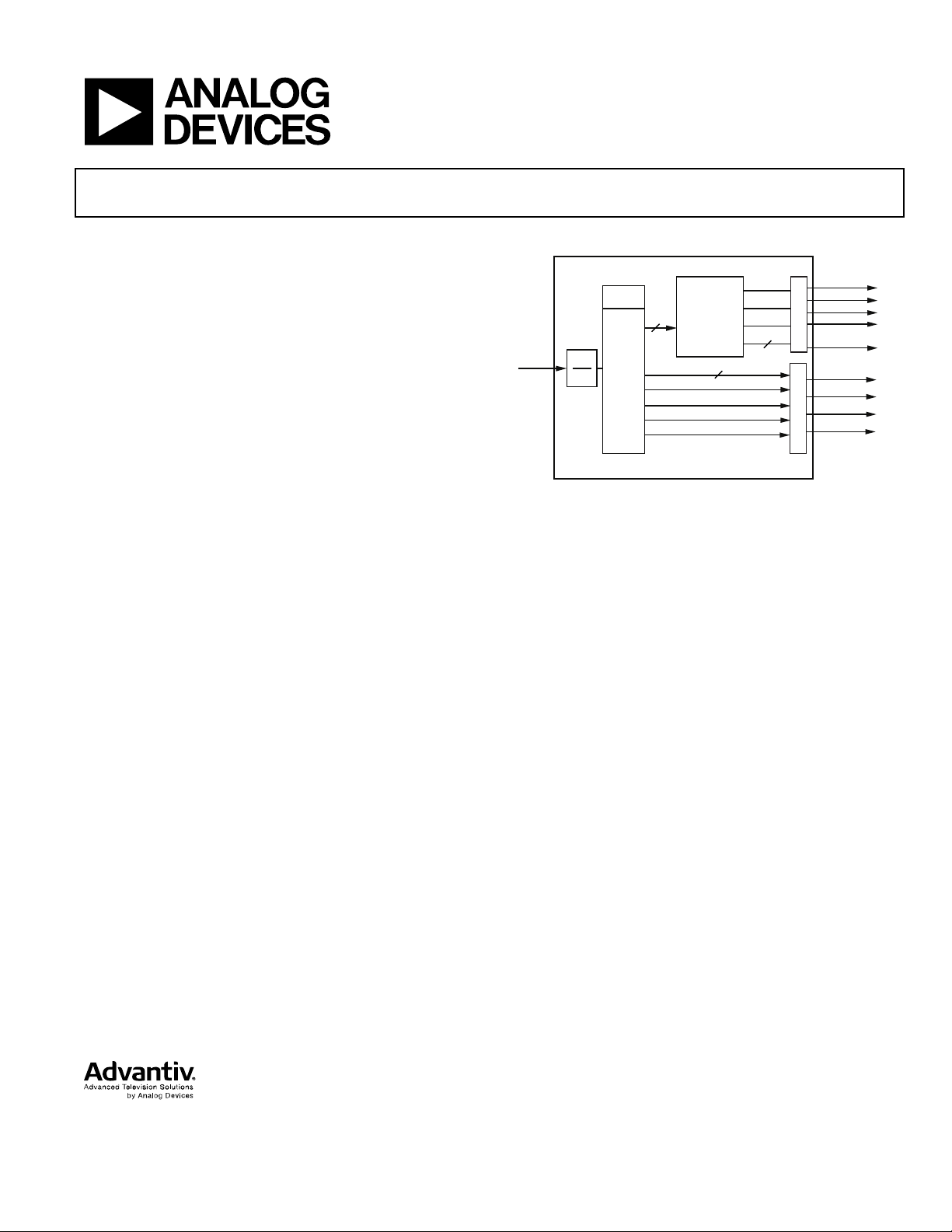
HDMI Rx
ADV7611
COMPONENT
PROCESSOR
36
OUTPUT MUX
FIELD/DE
LLC
DATA
MCLK
SCLK
LRCLK
LRCLK
AP
MCLK
SCLK
OUTPUT MUX
24-BIT
YCbCr/RGB
HS
VS/FIELD
DE
LLC
09305-001
Data Sheet
FEATURES
High-Definition Multimedia Interface (HDMI®) 1.4a features
supported
All mandatory and additional 3D video formats supported
Extended colorimetry, including sYCC601, Adobe RGB,
Adobe YCC 601, xvYCC extended gamut color
CEC 1.4-compatible
HDMI receiver
165 MHz maximum TMDS clock frequency
24-bit output pixel bus
High-bandwidth Digital Content Protection (HDCP) 1.4
support with internal HDCP keys
HDCP repeater support
Up to 127 KSVs supported
Integrated CEC controller
Programmable HDMI equalizer
5 V detect and Hot Plug assert for HDMI port
Audio support
SPDIF (IEC 60958-compatible) digital audio
HDMI audio extraction support
Advanced audio mute feature
General
Interrupt controller with two interrupt outputs
Standard identification (STDI) circuit
Highly flexible 24-bit pixel output interface
Internal EDID RAM
Any-to-any 3 × 3 color space conversion (CSC) matrix
2-layer PCB design supported
64-lead LQFP_EP, 10 mm × 10 mm package
Qualified for automotive applications
FUNCTIONAL BLOCK DIAGRAM
Figure 1.
APPLICATIONS
Projectors
Automotive
Video conferencing
HDTVs
AVR, HTiB
Soundbars
Video switches
Information furnished by Analog Devices is believed to be accurate and reliable. However, no
responsibility is assumed by Analog Devices for its use, nor for any infringements of p atents or other
rights of third parti es that may result from its use. Specification s subject to change without notice. No
license is granted by implication or otherwise under any patent or patent rights of Analog Devices.
One Technology Way, P.O. Box 9106, Norwood, MA 02062-9106, U.S.A.
Tel: 781.329.4700 www.analog.com
Page 2

ADV7611 Data Sheet
TABLE OF CONTENTS
Features .............................................................................................. 1
Applications ....................................................................................... 1
Functional Block Diagram .............................................................. 1
Revision History ............................................................................... 2
General Description ......................................................................... 3
Detailed Functional Block Diagram .......................................... 3
Specifications ..................................................................................... 4
Electrical Characteristics ............................................................. 4
Data and I2C Timing Characteristics ......................................... 5
Absolute Maximum Ratings ............................................................ 7
Package Thermal Performance ................................................... 7
ESD Caution .................................................................................. 7
Pin Configuration and Function Descriptions ............................. 8
Power Supply Sequencing .............................................................. 10
Power-Up Sequence ................................................................... 10
Power-Down Sequence .............................................................. 10
Functional Overview ...................................................................... 11
HDMI Receiver ........................................................................... 11
Component Processor ............................................................... 11
Other Features ............................................................................ 11
Pixel Input/Output Formatting .................................................... 12
Pixel Data Output Modes Features .......................................... 12
Outline Dimensions ....................................................................... 14
Ordering Guide .......................................................................... 14
Automotive Products ................................................................. 14
REVISION HISTORY
6/12—Rev. C t o R ev. D
Change to Pin 1 Description, Table 4 ............................................. 8
5/12—Rev. B t o R e v. C
Changes to Features Section............................................................ 1
Changes to General Description Section ...................................... 3
Added Endnote 3 (Table 1) ............................................................. 4
Deleted TDM Serial Timing Parameter (Table 2) ........................ 5
Deleted Figure 6 ................................................................................ 7
Changed Pin 48 Description (Tab le 4 ) .......................................... 9
Changes to HDMI Receiver and Other Features Sections ........ 11
Added Endnote 1 in Pixel Input/Output Formatting Section and
Endnote 1 to Table 5 ....................................................................... 12
Deleted Time-Division Multiplexed (TDM) Mode Section
and Figure 9 ..................................................................................... 13
Changes to P14 (Table 6) ............................................................... 13
Changes to Ordering Guide .......................................................... 14
Added HDMI Note ......................................................................... 16
6/11—Rev. A to Re v. B
Changes to Figure 7 .......................................................................... 1
5/11—Rev. 0 t o R e v. A
Changes to Features Section............................................................ 1
Changes to Ordering Guide .......................................................... 16
Added Automotive Products Section .......................................... 16
11/10—Revision 0: Initial Version
Rev. D | Page 2 of 16
Page 3
Data Sheet ADV7611
CONTROL
INTERFACE
I
2
C
CONTROL
AND DATA
PLL
EDID
REPEATER
CONTROLLER
HDCP
ENGINE
PACKET/
INFOFRAME
MEMORY
12
12
12
BACKEND
COLORSPACE
CONVERSION
OUTPUT FORMATTER
COMPONENT
PROCESSOR
5V DETECT
AND HPD
CONTROLLER
AUDIO
PROCESSOR
DATA
PREPROCESOR
AND COLOR
SPACE
CONVERSION
HDMI
PROCESSOR
PACKET
PROCESSOR
A
B
C
MUTE
INTERRUPT
CONTROLLER
(INT1,INT2)
P0 TO P7
*INT2 CAN BE ONLY OUTPUT ON ONE OF THE PINS: S CLK/INT2, MCLK/I NT2, OR HPA_A/ INT2.
XTALP
XTALN
SCL
SDA
CEC
RXA_5V
HPA_A/INT2*
DDCA_SDA
DDCA_SCL
RXA_C±
RXA_0±
RXA_1±
RXA_2±
P8 TO P15
P16 TO P23
LLC
HS
VS/FIELD/ALSB
DE
INT1
INT2*
AP
LRCLK
SCLK/INT2*
MCLK/INT2*
AUDIO OUTPUT FORMATTER
HDCP
EEPROM
SAMPLER
EQUALIZER
DPLL
CEC
CONTROLLER
ADV7611
09305-002
GENERAL DESCRIPTION
The ADV7611 is offered in automotive, professional (no
HDCP), and industrial versions. The operating temperature
o
range is −40
C to +85oC.
The UG-180 contains critical information that must be used in
conjunction with the ADV7611.
The ADV7611 is a high quality, single input HDMI®-capable
receiver. It incorporates an HDMI-capable receiver that
supports all mandatory 3D TV defined in HDMI 1.4a. The
ADV7611 supports formats up to UXGA 60 Hz at 8 bit.
It integrates a CEC controller that supports the capability
discovery and control (CDC) feature.
The ADV7611 has an audio output port for the audio data
extracted from the HDMI stream. The HDMI receiver has an
advanced mute controller that prevents audible extraneous
noise in the audio output.
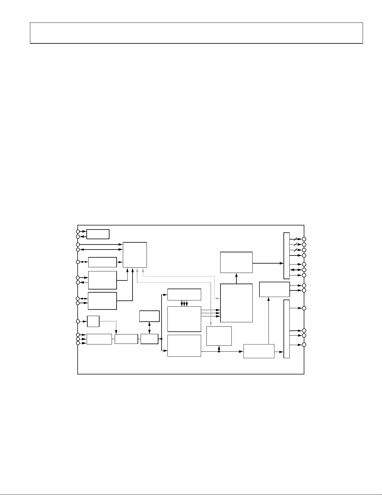
DETAILED FUNCTIONAL BLOCK DIAGRAM
The following audio formats are accessible:
• A stream from the I
2
S serializer (two audio channels)
• A stream from the S/PDIF serializer (two uncompressed
channels or N compressed channels, for example, AC3)
• DST stream
The HDMI port has dedicated 5 V detect and Hot Plug™ assert
pins. The HDMI receiver also includes an integrated equalizer
that ensures the robust operation of the interface with long cables.
The ADV7611 contains one main component processor (CP),
that processes the video signals from the HDMI receiver. It
provides features such as contrast, brightness and saturation
adjustments, STDI detection block, free run, and synchronization
alignment controls.
Fabricated in an advanced CMOS process, the ADV7611 is
provided in a 10 mm × 10 mm, 64-lead surface-mount LQFP_EP,
RoHS-compliant package and is specified over the −40°C to
+85°C temperature range.
Figure 2. Detailed Functional Block Diagram
Rev. D | Page 3 of 16
Page 4

ADV7611 Data Sheet
VIH
Other digital inputs
2
V
Output Capacitance
C
20
pF
Digital I/O Power Supply
DVDDIO
3.14
3.3
3.46
V
Comparator Supply Current
I
Power-Down Mode 1
1.3
1.7
mA
SPECIFICATIONS
At DVDD = 1.71 V to 1.89 V, DVDDIO = 3.14 V to 3.46 V, PVDD = 1.71 V to 1.89 V, TVDD = 3.14 V to 3.46 V, CVDD = 1.71 V to 1.89 V,
T
to T
MIN
ELECTRICAL CHARACTERISTICS
Table 1.
Parameter Symbol Test Conditions/Comments Min Typ Max Unit
DIGITAL INPUTS1
Input High Voltage VIH XTALN and XTALP 1.2 V
Input Low Voltage VIL XTALN a nd XTALP 0.4 V
VIL Other digital inputs 0.8 V
Input Current IIN
Other digital inputs ±10 µA
Input Capacitance CIN 10 pF
DIGITAL INPUTS (5 V TOLERANT)1, 2
Input High Voltage VIH 2.6 V
Input Low Voltage VIL 0.8 V
Input Current IIN −82 +82 µA
DIGITAL OUTPUTS1
Output High Voltage VOH 2.4 V
Output Low Voltage VOL 0.4 V
High Impedance Leakage
HPA_A/INT2 pin ±82 µA
Other 10 µA
POWER REQUIREMENTS
Digital Core Power Supply DVDD 1.71 1.8 1.89 V
= −40°C to +85°C, unless otherwise noted.
MAX
I
LEAK
Current
3, 4
OUT
RESET pin
±45 ±60 µA
VS/FIELD/ALSB pin ±35 ±60 µA
PLL Power Supply PVDD 1.71 1.8 1.89 V
Terminator Power Supply TVDD 3.14 3.3 3.46 V
Comparator Power Supply CVDD 1.71 1.8 1.89 V
Digital Core Supply Current I
Digital I/O Supply Current I
PLL Supply Current I
Terminator Supply Current I
Comparator Supply Current I
UXGA 60 Hz at 8 bit 95.7 188.1 mA
DVDD
UXGA 60 Hz at 8 bit 12.9 178.5 mA
DVDDIO
UXGA 60 Hz at 8 bit 30.7 36.9 mA
PVDD
UXGA 60 Hz at 8 bit 50.9 57.6 mA
TVDD
UXGA 60 Hz at 8 bit 95.8 114.4 mA
CVDD
POWER-DOWN CURRENTS3, 5
Digital Core Supply Current I
Digital I/O Supply Current I
PLL Supply Current I
Terminator Supply Current I
Power-Up Time t
1
Data guaranteed by characterization.
2
The following pins are 5 V tolerant: DDCA_SCL, DDC_SDA, and RXA_5V.
3
Data recorded during lab characterization.
4
Maximum current consumption values are recorded with maximum rated voltage supply levels, MoireX video pattern, and at maximum rated temperature.
5
Power-Down Mode 0 (IO map, Register 0x0C = 0x62), ring oscillator powered down (HDMI map, Register 0x48 = 0x01), and DDC pads off (HDMI map, Register 0x73 =
0x01).
Power-Down Mode 1 0.2 0.5 mA
DVDD_PD
DVDDIO_PD
Power-Down Mode 1 1.5 1.8 mA
PVDD_PD
Power-Down Mode 1 0.1 0.3 mA
TVDD_PD
CVDD_PD
25 ms
PWRUP
Power-Down Mode 1 1.3 1.7 mA
Rev. D | Page 4 of 16
Page 5

Data Sheet ADV7611
DATA AND I2C TIMING CHARACTERISTICS
Table 2.
Parameter Symbol Test Conditions/Comments Min Typ Max Unit
CLOCK AND CRYSTAL
Crystal Frequency, XTALP 28.63636 MHz
Crystal Frequency Stability ±50 ppm
LLC Frequency Range1 13.5 165 MHz
I2C PORTS
RESET FEATURE
CLOCK OUTPUTS
DATA AND CONTROL OUTPUTS3
I2S PORT, MASTER MODE
1
Maximum LLC frequency is limited by the clock frequency of UXGA 60 Hz at 8 bit.
2
Data guaranteed by characterization.
3
With the DLL block on output clock bypassed.
4
DLL bypassed on clock path.
5 I2
SCL Frequency 400 kHz
SCL Minimum Pulse Width High2 t
SCL Minimum Pulse Width Low2
Start Condition Hold Time2
Start Condition Setup Time2
SDA Setup Time2
SCL and SDA Rise Time2
SCL and SDA Fall Time2
Stop Condition Setup Time2
600 ns
1
1.3 μs
t
2
600 ns
t
3
600 ns
t
4
100 ns
t
5
300 ns
t
6
300 ns
t
7
0.6 μs
t
8
Reset Pulse Width 5 ms
45:55 55:45 % duty
LLC Mark-Space Ratio2
t
9:t10
cycle
Data Output Transition Time
2, 4
t
SCLK Mark-Space Ratio2
End of valid data to negative clock edge 1.0 2.2 ns
t
11
Negative clock edge to start of valid data 0.0 0.3 ns
12
45:55 55:45 % duty
t
15:t16
cycle
End of valid data to negative SCLK edge 10 ns
LRCLK Data Transition Time2
LRCLK Data Transition Time2
I2S Data Transition Time
I2S Data Transition Time
S is accessible via the AP pin.
2, 5
2, 5
t
17
Negative SCLK edge to start of valid data 10 ns
t
18
t
19
Negative SCLK edge to start of valid data 5 ns
t
20
End of valid data to negative SCLK edge 5 ns
Rev. D | Page 5 of 16
Page 6

ADV7611 Data Sheet
SDA
SCL
t
5
t
3
t
4
t
8
t
6
t
7
t
2
t
1
t
3
09305-003
t
9
LLC
t
11
t
12
t
10
P0 TO P23, HS ,
VS/FIELD/ALSB, DE
09305-004
SCLK
LRCLK
I
2
S
LEFT-JUSTIFIED
MODE
I
2
S
RIGHT-JUSTIFIED
MODE
I
2
S
I2S MODE
MSB M S B – 1
t
15
t
16
t
17
t
19
t
20
t
18
MSB
MSB – 1
LSBMSB
t
19
t
20
t
19
t
20
NOTES
1. I
2
S IS A SIGNAL ACCESSIBLE VIA THE AP P IN.
09305-005
Timing Diagrams
Figure 3. I
2
C Timing
Figure 4. Pixel Port and Control SDR Output Timing
Figure 5. I2S Timing
Rev. D | Page 6 of 16
Page 7

Data Sheet ADV7611
PVDD to GND
2.2 V
( )
TOTALJT
S
J
WΨTT ×+=
ABSOLUTE MAXIMUM RATINGS
Table 3.
Parameter Rating
DVDD to GND 2.2 V
DVDDIO to GND 4.0 V
CVDD to GND 2.2 V
TVDD to GND 4.0 V
Digital Inputs Voltage to GND GND − 0.3 V to DVDDIO + 0.3 V
5 V Tolerant Digital Inputs to
1
GND
5.3 V
Digital Outputs Voltage to GND GND − 0.3 V to DVDDIO + 0.3 V
XTALP, XTALN GND − 0.3 V to PVDD + 0.3 V
SCL/SDA Data Pins to DVDDIO
DVDDIO − 0.3 V to DVDDIO +
3.6 V
Maximum Junction Temperature
)
(T
J MAX
125°C
Storage Temperature Range −60°C to +150°C
Infrared Reflow Soldering (20 sec) 260°C
1
The following inputs are 3.3 V inputs but are 5 V tolerant: DDCA_SCL and
DDCA_SDA.
Stresses above those listed under Absolute Maximum Ratings
may cause permanent damage to the device. This is a stress
rating only; functional operation of the device at these or any
other conditions above those indicated in the operational
section of this specification is not implied. Exposure to absolute
maximum rating conditions for extended periods may affect
device reliability.
PACKAGE THERMAL PERFORMANCE
To reduce power consumption when using the ADV7611, the
user is advised to turn off the unused sections of the part.
Due to the printed circuit board (PCB) metal variation, and,
therefore, variation in PCB heat conductivity, the value of θ
JA
may differ for various PCBs.
The most efficient measurement solution is obtained using the
package surface temperature to estimate the die temperature
because this eliminates the variance associated with the θ
The maximum junction temperature (T
) of 125°C must not be
J MAX
value.
JA
exceeded. The following equation calculates the junction temperature using the measured package surface temperature and applies
only when no heat sink is used on the device under test (DUT):
where:
T
is the package surface temperature (°C).
S
= 0.4°C/W for the 64-lead LQFP_EP.
Ψ
JT
= ((PVDD × I
W
TOTAL
I
) + (DVDD × I
CVDD
) + (0.05 × TVDD × I
PVDD
) + (DVDDIO × I
DVDD
DVDDIO
) + (CVDD ×
TVDD
))
where 0.05 is 5% of the TVDD power that is dissipated on the
part itself.
ESD CAUTION
Rev. D | Page 7 of 16
Page 8

ADV7611 Data Sheet
AP
VS/FIELD/ALSB
HS
DE
DVDDIO
P0
P1
P2
DVDD
P3
P4
P5
P6
P7
DVDDIO
P8
RXA_5V
DDCA_SDA
DDCA_SCL
CEC
DVDD
XTALN
XTALP
PVDD
RESET
INT1
SDA
SCL
DVDD
MCLK/INT2
LRCLK
SCLK/INT2
P21
P20
P19
P18
P17
P16
DVDDIO
DVDD
LLC
P15
P14
P13
P12
P11
P10
P9
HPA_A/INT2
CVDD
RXA_C–
RXA_C+
TVDD
RXA_0–
RXA_0+
TVDD
RXA_1–
RXA_1+
TVDD
RXA_2–
RXA_2+
CVDD
P23
P22
2
3
4
7
6
5
1
8
9
10
12
13
14
15
16
11
47
46
45
42
43
44
48
41
40
39
37
36
35
34
33
38
17
18 19 20 21
22 23 24 25 26 27 28 29 30 31 32
64
63 62
61
60 59 58 57 56 55 54 53 52 51 50 49
ADV7611
TOP VIEW
(Not to S cale)
PIN 1
INDICATOR
NOTES
1. CONNECT EXPOSED PAD (PIN0) TO GROUND (BOTTOM).
09305-008
1
HPA_A/INT2
Miscellaneous digital
A dual function pin that can be configured to output a Hot Plug assert signal (for
11
TVDD
Power
Terminator Supply Voltage (3.3 V).
22
P16
Digital video output
Video Pixel Output Port.
PIN CONFIGURATION AND FUNCTION DESCRIPTIONS
Figure 6. Pin Configuration
Table 4. Pin Function Descriptions
Pin No. Mnemonic Type Description
0 GND Ground Ground.
HDMI Port A) or an Interrupt 2 signal. This pin is 5 V tolerant.
2 CVDD Power HDMI Analog Block Supply Voltage (1.8 V ).
3 RXA_C− HDMI input Digital Input Clock Complement of Port A in the HDMI Interface.
4 RXA_C+ HDMI input Digital Input Clock True of Port A in the HDMI Interface.
5 TVDD Power Terminator Supply Voltage (3.3 V).
6 RXA_0− HDMI input Digital Input Channel 0 Complement of Port A in the HDMI Interface.
7 RXA_0+ HDMI input Digital Input Channel 0 True of Port A in the HDMI Interface.
8 TVDD Power Terminator Supply Voltage (3.3 V).
9 RXA_1− HDMI input Digital Input Channel 1 Complement of Port A in the HDMI Interface.
10 RXA_1+ HDMI input Digital Input Channel 1 True of Port A in the HDMI Interface.
12 RXA_2− HDMI input Digital Input Channel 2 Complement of Port A in the HDMI Interface.
13 RXA_2+ HDMI input Digital Input Channel 2 True of Port A in the HDMI Interface.
14 CVDD Power HDMI Analog Block Supply Voltage (1.8 V).
15 P23 Digital video output Video Pixel Output Port.
16 P22 Digital video output Video Pixel Output Port.
17 P21 Digital video output Video Pixel Output Port.
18 P20 Digital video output Video Pixel Output Port.
19 P19 Digital video output Video Pixel Output Port.
20 P18 Digital video output Video Pixel Output Port.
21 P17 Digital video output Video Pixel Output Port.
23 DVDDIO Power Digital I/O Supply Voltage (3.3 V).
24 DVDD Power Digital Core Supply Voltage (1.8 V).
Rev. D | Page 8 of 16
Page 9

Data Sheet ADV7611
33
P8
Digital video output
Video Pixel Output Port.
39
P3
Digital video output
Video Pixel Output Port.
44
DVDDIO
Power
Digital I/O Supply Voltage (3.3 V).
48
AP
Miscellaneous digital
64
RXA_5V
HDMI input
5 V Detect Pin for Port A in the HDMI Interface.
Pin No. Mnemonic Type Description
25 LLC Digital video output Line-Locked Output Clock for the Pixel Data (Range is 13.5 MHz to 162.5 MHz).
26 P15 Digital video output Video Pixel Output Port.
27 P14 Digital video output Video Pixel Output Port.
28 P13 Digital video output Video Pixel Output Port.
29 P12 Digital video output Video Pixel Output Port.
30 P11 Digital video output Video Pixel Output Port.
31 P10 Digital video output Video Pixel Output Port.
32 P9 Digital video output Video Pixel Output Port.
34 DVDDIO Power Digital I/O Supply Voltage (3.3 V).
35 P7 Digital video output Video Pixel Output Port.
36 P6 Digital video output Video Pixel Output Port.
37 P5 Digital video output Video Pixel Output Port.
38 P4 Digital video output Video Pixel Output Port.
40 DVDD Power Digital Core Supply Voltage (1.8 V).
41 P2 Digital video output Video Pixel Output Port.
42 P1 Digital video output Video Pixel Output Port.
43 P0 Digital video output Video Pixel Output Port.
45 DE Miscellaneous digital DE (data enable) is a signal that indicates active pixel data.
46 HS Digital video output HS is a horizontal synchronization output signal.
47
VS/FIELD/ALS
B
49 SCLK/INT2 Miscellaneous digital
50 LRCLK Miscellaneous digital Audio Left/Right Clock.
51 MCLK/INT2 Miscellaneous digital
52 DVDD Power Digital Core Supply Voltage (1.8 V).
53 SCL Miscellaneous digital I2C Port Serial Clock Input. SCL is the clock line for the control port.
54 SDA Miscellaneous digital I2C Port Serial Data Input/Output Pin. SDA is the data line for the control port.
55 INT1 Miscellaneous digital
56
RESET
57 PVDD Power PLL Supply Voltage (1.8 V).
58 XTALP Miscellaneous analog
59 XTALN Miscellaneous analog Crystal Input. Input pin for 28.63636 MHz crystal.
60 DVDD Power Digital Core Supply Voltage (1.8 V).
61 CEC Digital input/output Consumer Electronic Control Channel.
62 DDCA_SCL HDMI input HDCP Slave Serial Clock Port A. DDCA_SCL is a 3.3 V input that is 5 V tolerant.
63 DDCA_SDA HDMI input HDCP Slave Serial Data Port A. DDCA_SDA is a 3.3 V input that is 5 V tolerant.
Digital input/output
Miscellaneous digital
VS is a vertical synchronization output signal. FIELD is a field synchronization output
signal in all interlaced video modes. VS or FIELD can be configured for this pin. The
ALSB allows selection of the I
Audio Output Pin. Pin can be configured to output S/PDIF digital audio output
(S/PDIF) or I
2
S.
2
C address.
A dual function pin that can be configured to output an audio serial clock or an
Interrupt 2 signal.
A dual function pin that can be configured to output an audio master clock or an
Interrupt 2 signal.
Interrupt. This pin can be active low or active high. When status bits change, this pin is
triggered. The events that trigger an interrupt are under user configuration.
System Reset Input. Active low. A minimum low reset pulse width of 5 ms is required
to reset the ADV7611 circuitry.
Input Pin for 28.63636 MHz Crystal or an External 1.8 V, 28.63636 MHz Clock Oscillator
Source to Clock the ADV7611.
Rev. D | Page 9 of 16
Page 10

ADV7611 Data Sheet
3.3V
POWER SUPPLY (V)
1.8V
3.3V SUPPLIES
1.8V SUPPLIES
1.8V SUPPLIES
POWER-UP
3.3V SUPPLIES
POWER-UP
09305-007
POWER SUPPLY SEQUENCING
POWER-UP SEQUENCE
The recommended power-up sequence of the ADV7611 is to
power up the 3.3 V supplies first, followed by the 1.8 V supplies.
Reset should be held low while the supplies are powered up.
Alternatively, the ADV7611 may be powered up by asserting all
supplies simultaneously. In this case, care must be taken while the
supplies are being established to ensure that a lower rated supply
does not go above a higher rated supply level.
POWER-DOWN SEQUENCE
The ADV7611 supplies may be deasserted simultaneously as
long as a higher rated supply does not go below a lower rated
supply.
Figure 7. Recommended Power-Up Sequence
Rev. D | Page 10 of 16
Page 11

Data Sheet ADV7611
FUNCTIONAL OVERVIEW
HDMI RECEIVER
The receiver supports all mandatory and many optional 3D
formats. It supports HDTV formats up to UXGA at 8 bit.
The HDMI-compatible receiver on the ADV7611 incorporates
programmable equalization of the HDMI data signals. This
equalization compensates for the high frequency losses inherent
in HDMI and DVI cabling, especially at longer lengths and higher
frequencies. It is capable of equalizing for cable lengths up to
30 meters to achieve robust receiver performance.
With the inclusion of HDCP, displays can receive encrypted
video content. The HDMI interface of the ADV7611 allows for
authentication of a video receiver, decryption of encoded data
at the receiver, and renewability of that authentication during
transmission, as specified by the HDCP 1.4 protocol.
The ADV7611 has a synchronization regeneration block used
to regenerate the DE based on the measurement of the video
format being displayed and to filter the horizontal and vertical
synchronization signals to prevent glitches. The HDMI receiver
also supports TERC4 error detection, used for detection of
corrupted HDMI packets following a cable disconnect.
The HDMI receiver contains an audio mute controller that
can detect a variety of conditions that may result in audible
extraneous noise in the audio output. On detection of these
conditions, the audio signal can be ramped to prevent audio
clicks or pops. Audio output can be formatted to LPCM and
IEC 61937.
The HDMI receiver features include:
• 162.5 MHz (UXGA at 8 bit) maximum TMDS clock
frequency
• 3D format support defined in HDMI 1.4a specification
• Integrated equalizer for cable lengths up to 30 meters
• HDCP 1.4
• Internal HDCP keys
• PCM audio packet support
• Repeater support
• Internal EDID RAM
• Hot Plug assert output pin for an HDMI port
• CEC controller
COMPONENT PROCESSOR
The ADV7611 has an any-to-any 3 × 3 CSC matrix. The CSC
block is placed at the back of the CP section. CSC enables
YPrPb-to-RGB and RGB-to-YCrCb conversions. Many other
standards of color space can be implemented using the color
space converter.
CP features include:
• 525i, 625i, 525p, 625p, 720p, 1080i, 1080p, and other
formats
• Manual adjustments including gain (contrast) and
offset (brightness), hue, and saturation
• Free run output mode that provides stable timing when no
video input is present
• 162.5 MHz processing rate
• Contrast, brightness, hue, and saturation controls
• Standard identification enabled by STDI block
• RGB that can be color space converted to YCrCb and
decimated to a 4:2:2 format for video-centric back end IC
interfacing
• DE output signal supplied for direct connection to an
HDMI/DVI transmitter
OTHER FEATURES
The ADV7611 has HS, VS, FIELD, and DE output signals with
programmable position, polarity, and width.
The ADV7611 has programmable interrupt request output pins,
including INT1 and INT2 (INT2 is accessible only via one of
following pins: MCLK/INT2, SCLK/INT2, or HPA_A/INT2).
It also features a low power-down mode. The I
the main map is 0x98 after reset. This can be changed after reset
to 0x9A if pullup is attached to VS/FIELD/ALSB pin and I
command SAMPLE_ALSB is issued. Refer to the Register
Access and Serial Ports Description section in the UG-180.
The ADV7611 is provided in a 10 mm × 10 mm, RoHS-compliant
LQFP_EP package, and is specified over the −40°C to +85°C
temperature range.
2
C address of
2
C
Rev. D | Page 11 of 16
Page 12

ADV7611 Data Sheet
P21
High-Z
Y1, Cb1, Cr1
High-Z
Y1
R5
P16
High-Z
High-Z
High-Z
Cb0, Cr0
R0
P10
Y2, Cb2, Cr2
Y6, Cb6, Cr6
Y2
Y6
G2
P4
High-Z
High-Z
Cb4, Cr4
Cb8, Cr8
B4
PIXEL INPUT/OUTPUT FORMATTING
The output section of the ADV7611 is highly flexible. The pixel
output bus can support up to 24-bit 4:4:4 YCrCb. The pixel data
supports both single and double data rates modes. In SDR mode, a
16-/24-bit 4:2:2 or 24-bit 4:4:4 output is possible. In DDR mode
1
,
the pixel output port can be configured in an 8-/12-bit 4:2:2 YCrCb
or 24-bit 4:4:4 RGB.
Bus rotation is supported. Ta ble 5 and Table 6 outline the different
output formats that are supported. All output modes are controlled
2
via I
C.
1
DDR mode is only supported only up to 50 MHz (an equivalent to data rate
clocked 100 MHz clock in SDR mode).
Table 5. SDR 4:2:2 and 4:4:4 Output Modes
SDR 4:2:2 SDR 4:4:4
OP_FORMAT_SEL[7:0] 0x01 0x0A1 0x80 0x8A 0x40
8-Bit SDR
ITU-R BT.656
Pixel Output
P23 High-Z Y3, Cb3, Cr3 High-Z Y3 R7
P22 High-Z Y2, Cb2, Cr2 High-Z Y2 R6
Mode 0
12-Bit SDR
ITU-R BT.656
Mode 2
16-Bit SDR
ITU-R BT.656 4:2:2
Mode 0
PIXEL DATA OUTPUT MODES FEATURES
The output pixel port features include:
• 8-/12-bit ITU-R BT.656 4:2:2 YCrCb with embedded time
codes and/or HS, VS, and FIELD output signals
• 16-/24-bit YCrCb with embedded time codes and/or HS
and VS/FIELD pin timing
• 24-bit YCrCb/RGB with embedded time codes and/or HS
and VS/FIELD pin timing
• DDR 8-/12-bit 4:2:2 YCrCb
• DDR 24-bit 4:4:4 RGB
24-Bit SDR
ITU-R BT.656 4:2:2
Mode 2
24-Bit SDR 4:4:4
Mode 0
P20 High-Z Y0, Cb0, Cr0 High-Z Y0 R4
P19 High-Z High-Z High-Z Cb3, Cr3 R3
P18 High-Z High-Z High-Z Cb2, Cr2 R2
P17 High-Z High-Z High-Z Cb1, Cr1 R1
P15 Y7, Cb7, Cr7 Y11, Cb11, Cr11 Y7 Y11 G7
P14 Y6, Cb6, Cr6 Y10, Cb10, Cr10 Y6 Y10 G6
P13 Y5, Cb5, Cr5 Y9, Cb9, Cr9 Y5 Y9 G5
P12 Y4, Cb4, Cr4 Y8, Cb8, Cr8 Y4 Y8 G4
P11 Y3, Cb3, Cr3 Y7, Cb7, Cr7 Y3 Y7 G3
P9 Y1, Cb1, Cr1 Y5, Cb5, Cr5 Y1 Y5 G1
P8 Y0, Cb0, Cr0 Y4, Cb4, Cr4 Y0 Y4 G0
P7 High-Z High-Z Cb7, Cr7 Cb11, Cr11 B7
P6 High-Z High-Z Cb6, Cr6 Cb10, Cr10 B6
P5 High-Z High-Z Cb5, Cr5 Cb9, Cr9 B5
P3 High-Z High-Z Cb3, Cr3 Cb7, Cr7 B3
P2 High-Z High-Z Cb2, Cr2 Cb6, Cr6 B2
P1 High-Z High-Z Cb1, Cr1 Cb5, Cr5 B1
P0 High-Z High-Z Cb0, Cr0 Cb4, Cr4 B0
1
Modes 0x00 and 0x0A require additional writes to IO Map Register 0x19[7:6] = 2’b11 and IO Map Register 0x33[6] = 1
Rev. D | Page 12 of 16
Page 13

Data Sheet ADV7611
P18
High-Z
High-Z
High-Z
High-Z
R2-0
R2-1
P13
Cb5, Cr5
Y5
Cb9, Cr9
Y9
G5-0
G5-1
P7
High-Z
High-Z
High-Z
High-Z
B7-0
B7-1
Table 6. DDR 4:2:2 and 4:4:4 Output Modes
DDR 4:2:2 Mode (Clock/2) DDR 4:2:2 Mode (Clock/2) DDR 4:4:4 Mode (Clock/2)
OP_FORMAT_SEL[7:0] 0x20 0x2A 0x60
8-Bit DDR ITU-656
(Clock/2 Output) 4:2:2 Mode 0
12-Bit DDR ITU-656
(Clock/2 Output) 4:2:2 Mode 2
24-Bit DDR RGB
(Clock/2 Output)
Pixel Output Clock Rise Clock Fall Clock Rise Clock Fall Clock Rise Clock Fall
P23 High-Z High-Z Cb3, Cr3 Y3 R7-0 R7-1
P22 High-Z High-Z Cb2, Cr2 Y2 R6-0 R6-1
P21 High-Z High-Z Cb1, Cr1 Y1 R5-0 R5-1
P20 High-Z High-Z Cb0, Cr0 Y0 R4-0 R4-1
P19 High-Z High-Z High-Z High-Z R3-0 R3-1
P17 High-Z High-Z High-Z High-Z R1-0 R1-1
P16 High-Z High-Z High-Z High-Z R0-0 R0-1
P15 Cb7, Cr7 Y7 Cb11, Cr11 Y11 G7-0 G7-1
P14 Cb6, Cr6 Y6 Cb10, Cr10 Y10 G6-0 G6-1
P12 Cb4, Cr4 Y4 Cb8, Cr8 Y8 G4-0 G4-1
P11 Cb3, Cr3 Y3 Cb7, Cr7 Y7 G3-0 G3-1
P10 Cb2, Cr2 Y2 Cb6, Cr6 Y6 G2-0 G2-1
P9 Cb1, Cr1 Y1 Cb5, Cr5 Y5 G1-0 G1-1
P8 Cb0, Cr0 Y0 Cb4, Cr4 Y4 G0-0 G0-1
1, 2
P6 High-Z High-Z High-Z High-Z B6-0 B6-1
P5 High-Z High-Z High-Z High-Z B5-0 B5-1
P4 High-Z High-Z High-Z High-Z B4-0 B4-1
P3 High-Z High-Z High-Z High-Z B3-0 B3-1
P2 High-Z High-Z High-Z High-Z B2-0 B2-1
P1 High-Z High-Z High-Z High-Z B1-0 B1-1
P0 High-Z High-Z High-Z High-Z B0-0 B0-1
1
-0 = even samples.
2
-1 = odd samples.
Rev. D | Page 13 of 16
Page 14

ADV7611 Data Sheet
COMPLIANT TO JEDEC STANDARDS MS-026-BCD- HD
1
16
17
32 32
49
64
48
33
12.20
12.00 SQ
11.80
10.20
10.00 SQ
9.80
1
16
17
49 64
48
33
PIN 1
TOP VIEW
(PINS DO W N)
BOTTOM VIEW
(PINS UP)
EXPOSED
PAD
06-12-2012-A
VIEW A
1.60
MAX
SEATING
PLANE
0.75
0.60
0.45
1.00 REF
0.15
0.05
0.08
COPLANARITY
7°
0°
0.20
0.09
VIEW A
ROTATED 90° CCW
1.45
1.40
1.35
0.27
0.22
0.17
0.50
LEAD PIT CH
7.50
REF SQ
FOR PROP E R CONNECTION OF
THE EXPOSED PAD, REFER TO
THE PIN CO NFIGURATI ON AND
FUNCTIO N DE S CRIPTIONS
SECTION OF THIS DATA SHEET.
5.10
5.00 SQ
4.90
4
OUTLINE DIMENSIONS
Figure 8. 64-Lead Low Profile Quad Flat Package (LQFP_EP)
SW-64-2
Dimensions shown in millimeters
ORDERING GUIDE
1, 2
Model
ADV7611BSWZ −40°C to +85°C 64-Lead LQFP_EP SW-64-2
ADV7611BSWZ-RL
ADV7611BSWZ-P
ADV7611BSWZ-P-RL
ADV7611WBSWZ −40°C to +85°C 64-Lead LQFP_EP SW-64-2
ADV7611WBSWZ-RL
EVA L-ADV7611EB1Z Evaluation Board with HDCP Keys
EVA L-ADV7611EB2Z Evaluation Board Without HDCP Keys
1
Z = RoHS Compliant Part.
2
W = Qualified for Automotive Parts.
3
13” Tape and Reel.
4
Non-HDCP version.
AUTOMOTIVE PRODUCTS
The ADV7611W models are available with controlled manufacturing to support the quality and reliability requirements of automotive
applications. Note that these automotive models may have specifications that differ from the commercial models; therefore, designers
should review the Specifications section of this data sheet carefully. Only the automotive grade products shown are available for use in
automotive applications. Contact your local Analog Devices, Inc., account representative for specific product ordering information and to
obtain the specific Automotive Reliability report for this model.
Notes Temperature Range Package Description Package Option
3
−40°C to +85°C 64-Lead LQFP_EP SW-64-2
−40°C to +85°C 64-Lead LQFP_EP SW-64-2
3
−40°C to +85°C 64-Lead LQFP_EP SW-64-2
3
−40°C to +85°C 64-Lead LQFP_EP SW-64-2
Rev. D | Page 14 of 16
Page 15

Data Sheet ADV7611
NOTES
Rev. D | Page 15 of 16
Page 16

ADV7611 Data Sheet
©2010-2012 Analog Devices, Inc. All rights reserved. Trademarks and
NOTES
HDMI, the HDMI Logo, and High-Definition Multimedia Interface are trademarks or registered trademarks of HDMI Licensing LLC in the United States and other
countries.
registered trademarks are the property of their respective owners.
D09305-0-6/12(D)
Rev. D | Page 16 of 16
 Loading...