

165 MHz, High Performance
Data Sheet
FEATURES
General
Incorporates HDMI v1.4 features, including
3D video support
165 MHz supports all video formats up to 1080p
and UXGA
Supports gamut metadata packet transmission
Integrated CEC buffer/controller
Compatible with DVI v1.0 and HDCP v1.4
Video/audio inputs accept logic levels from 1.8 V to 3.3 V
Digital video
3D video ready
Programmable, 2-way color space converter
Supports RGB, YCbCr, and DDR
Supports ITU-656-based embedded syncs
Automatic input video format timing detection (CEA-861-E)
Digital audio
Supports standard S/PDIF for stereo linear pulse code
modulation (LPCM) or compressed audio up to 192 kHz
High bit rate (HBR) audio
8-channel uncompressed LPCM I
Special features for easy system design
5 V tolerant I
2
C and Hot Plug™ detect (HPD) I/Os,
no extra device needed
No audio master clock needed for supporting S/PDIF
2
and I
S
On-chip MPU with I
2
C master performs HDCP operations
and EDID reading operations
On-chip MPU reports HDMI events through interrupts
and registers
APPLICATIONS
Gaming consoles
PCs
DVD players and recorders
Digital set-top boxes
A/V receivers
2
S audio up to 192 kHz
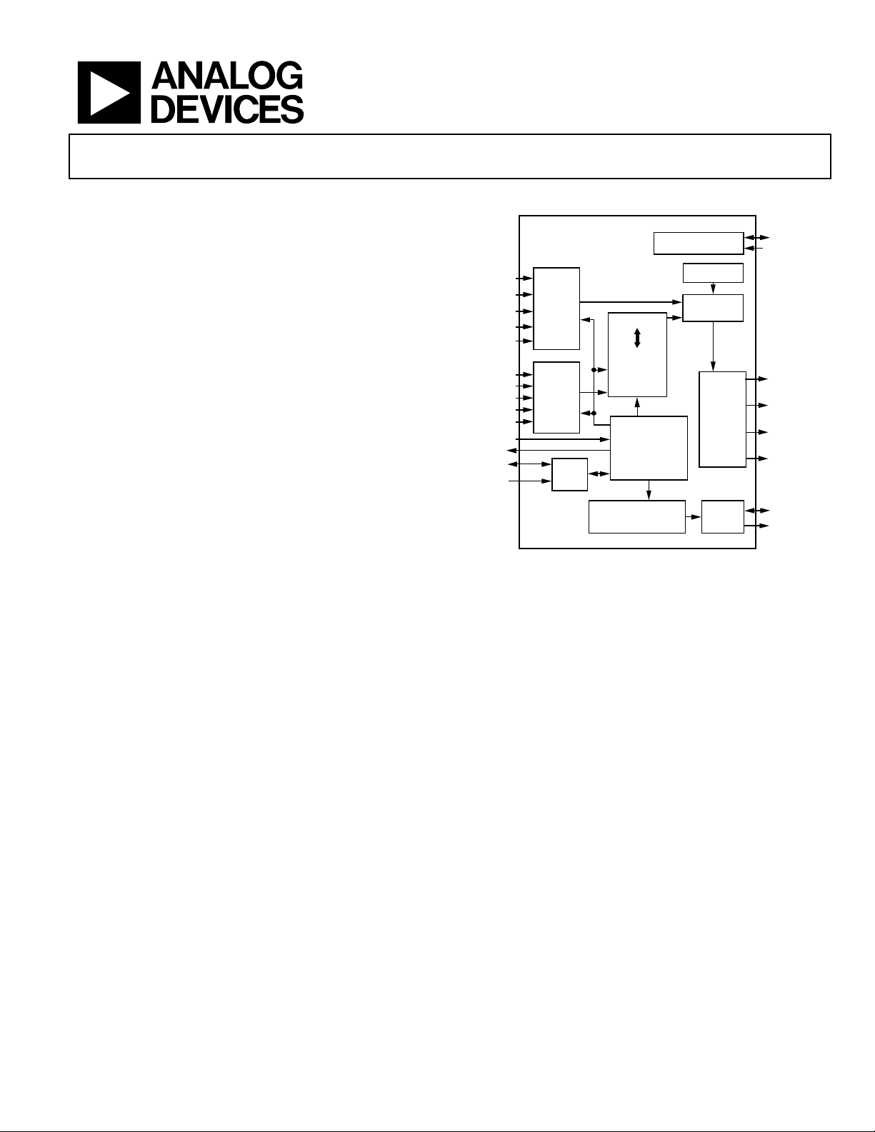
HDMI Transmitter
ADV7513
FUNCTIONAL BLOCK DIAGRAM
CEC
CEC_CLK
TX0+/TX0–
TX1+/TX1–
TX2+/TX2–
TXC+/TXC–
DDCSDA
DDCSCL
2
S audio.
4:2:2
4:4:4
AND
COLOR
SPACE
LOGIC
HDCP
AND EDID
CEC CONTROL LER/
BUFFER
HDCP KEYS
HDCP
ENCRYPTION
TMDS
OUTPUTS
2
I
C
MASTER
SPDIF
I2S[3:0]
MCLK
LRCLK
SCLK
D[23:0]
VSYNC
HSYNC
DE
CLK
HPD
INT
SDA
SCL
ADV7513
AUDIO
DATA
CAPTURE
VIDEO
DATA
CAPTURE
I
SLAVE
CONVERTER
REGISTERS AND
CONFIGURATION
2
C
MICROCONTROLLER
Figure 1.
GENERAL DESCRIPTION
The ADV7513 is a 165 MHz, High-Definition Multimedia
Interface (HDMI®) transmitter that is ideal for DVD players/
recorders, digital set-top boxes, A/V receivers, gaming consoles,
and PCs.
The digital video interface contains an HDMI v1.4/DVI v1.0compatible transmitter and supports all HDTV formats. The
ADV7513 supports HDMI v1.4-specific features, including 3D
video. The ADV7513 also supports x.v.Color™, high bit rate (HBR)
audio, and the programmable auxiliary video information (AVI)
InfoFrame features. With the inclusion of HDCP, the ADV7513
allows the secure transmission of protected content as specified
by the HDCP v1.4 protocol.
The ADV7513 supports both S/PDIF and 8-channel I
Its high fidelity 8-channel I
or 7.1 surround audio up to 768 kHz. The S/PDIF interface can
carry compressed audio, including Dolby® Digital, DTS®, and
THX®. Fabricated in an advanced CMOS process, the ADV7513
is provided in a 64-lead LQFP surface-mount plastic package
with exposed pad and is specified over the −25°C to +85°C
temperature range.
2
S interface can transmit either stereo
10225-001
Rev. 0
Information furnished by Analog Devices is believed to be accurate and reliable. However, no
responsibility is assumed by Analog Devices for its use, nor for any infringements of patents or other
rights of third parties that may result from its use. Specifications subject to change without notice. No
license is granted by implication or otherwise under any patent or patent rights of Analog Devices.
Trademarks and registered trademarks are the property of their respective owners.
One Technology Way, P.O. Box 9106, Norwood, MA 02062-9106, U.S.A.
Tel: 781.329.4700 www.analog.com
Fax: 781.461.3113 ©2011 Analog Devices, Inc. All rights reserved.

ADV7513 Data Sheet
TABLE OF CONTENTS
Features .............................................................................................. 1
Applications ....................................................................................... 1
Functional Block Diagram .............................................................. 1
General Description ......................................................................... 1
Revision History ............................................................................... 2
Specifications ..................................................................................... 3
Electrical Specifications ............................................................... 3
REVISION HISTORY
11/11—Revision 0: Initial Version
Absolute Maximum Ratings ............................................................5
Explanation of Test Levels ............................................................5
ESD Caution...................................................................................5
Pin Configuration and Function Descriptions ..............................6
Applications Information .................................................................8
Design Resources ..........................................................................8
Outline Dimensions ..........................................................................9
Ordering Guide .............................................................................9
Rev. 0 | Page 2 of 12
Data Sheet ADV7513
SPECIFICATIONS
ELECTRICAL SPECIFICATIONS
Table 1.
Parameter Symbol Temp Test Level1 Min Typ Max Unit
DIGITAL INPUTS
Data Inputs, Video and Audio, CEC_CLK
Input Voltage, High VIH Full VI 1.35 3.5 V
Input Voltage, Low VIL Full VI −0.3 +0.7 V
Input Capacitance 25°C VIII 1.0 1.5 pF
CEC_CLK Frequency2 Full VIII 3 12 100 MHz
CEC_CLK Accuracy Full VIII −2 +2 %
DDC I2C Lines (DDCSDA, DDCSCL)
Input Voltage, High VIH Full IV 1.4 5.5 V
Input Voltage, Low VIL Full IV −0.3 +0.7 V
I2C Lines (SDA, SCL)
Input Voltage, High VIH Full VI 1.4 5.5 V
Input Voltage, Low VIL Full VI −0.3 +0.7 V
CEC Pin
Input Voltage, High VIH Full VI 2.0 5.5 V
Input Voltage, Low VIL Full VI −0.3 +0.8 V
Output Voltage, High VOH Full VI 2.5 3.63 V
Output Voltage, Low VOL Full VI −0.3 +0.6 V
HPD Pin
Input Voltage, High VIH Full VI 1.3 5.5 V
Input Voltage, Low VIL Full VI −0.3 +0.8 V
THERMAL CHARACTERISTICS
Thermal Resistance
Junction-to-Case θJC Full V 20 °C/W
Junction-to-Ambient θJA Full V 43 °C/W
Ambient Temperature Full V −25 +25 +85 °C
DC SPECIFICATIONS
Input Leakage Current IIL 25°C VI −1 +1 μA
POWER SUPPLY
1.8 V Supply Voltage (DVDD, AVDD,
PVDD, BGVDD)
3.3 V Supply Voltage (DVDD_3V) Full IV 3.15 3.3 3.45 V
Power-Down Current 25°C IV 300 μA
Transmitter Total Power3
At 1.8 V Full VI 256 mW
At 3.3 V Full VI 1 mW
AC SPECIFICATIONS
TMDS Output Clock Frequency 25°C IV 20 165 MHz
TMDS Output Clock Duty Cycle 25°C IV 48 52 %
Input Video Clock Frequency Full IV 165 MHz
Input Video Data Setup Time4 t
Input Video Data Hold Time4 t
TMDS Differential Swing 25°C VII 800 1100 1200 mV
Differential Output Timing
Low-to-High Transition Time 25°C VII 75 95 ps
High-to-Low Transition Time 25°C VII 75 95 ps
VSYNC and HSYNC Delay
From DE Falling Edge 25°C IV 1 UI5
To DE Rising Edge 25°C IV 1 UI5
Full IV 1.71 1.8 1.90 V
Full IV 1.8 ns
VSU
Full IV 1.3 ns
VHLD
Rev. 0 | Page 3 of 12
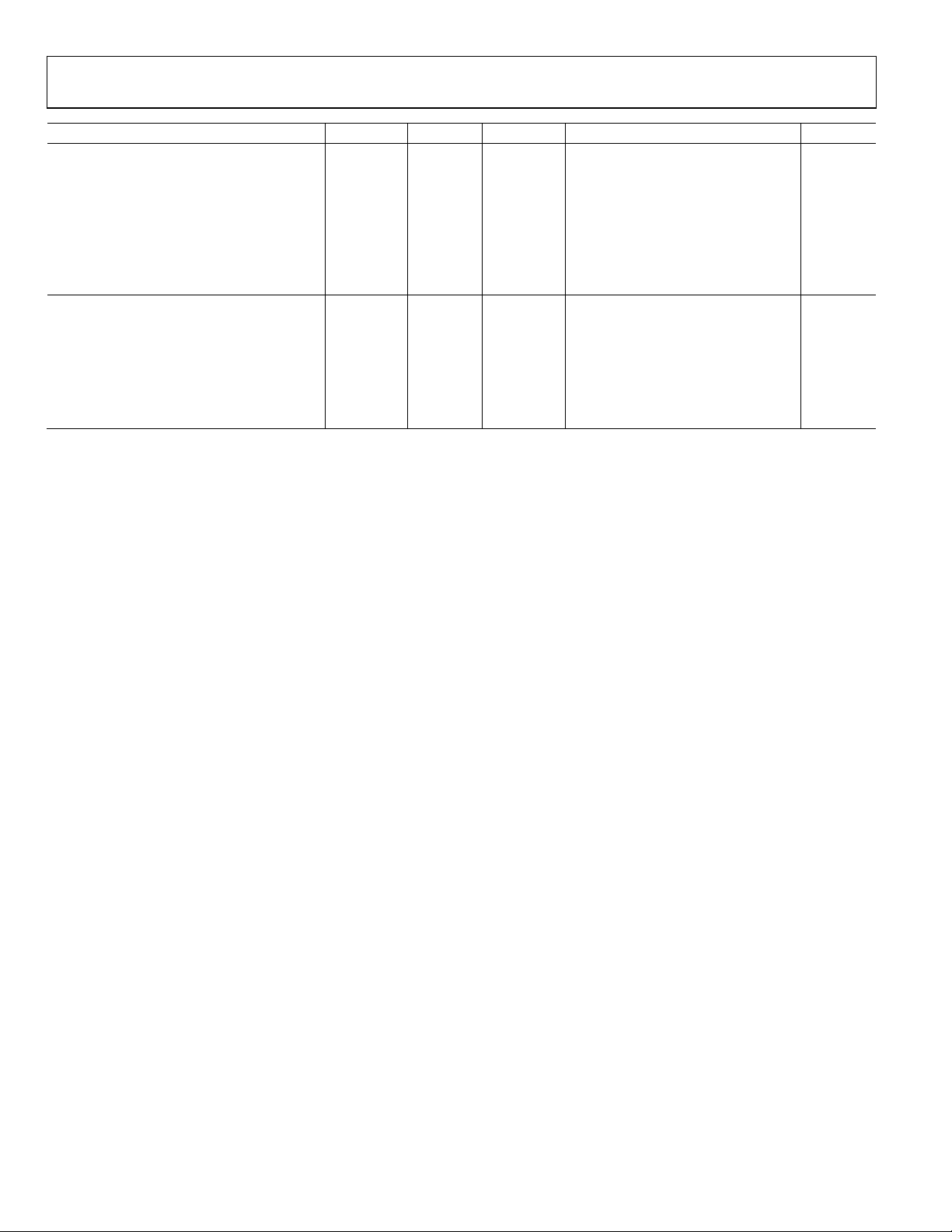
ADV7513 Data Sheet
Parameter Symbol Temp Test Level1 Min Typ Max Unit
AUDIO AC TIMING
SCLK Duty Cycle
N/2 Is an Even Number Full IV 40 50 60 %
N/2 Is an Odd Number Full IV 49 50 51 %
I2S[3:0], S/PDIF Setup Time t
I2S[3:0], S/PDIF Hold Time t
LRCLK Setup Time t
LRCLK Hold Time t
I2C INTERFACE
SCL Clock Frequency Full 400 kHz
SDA Setup Time t
SDA Hold Time t
Setup Time for Start Condition t
Hold Time for Start Condition t
Setup Time for Stop Condition t
1
See the Explanation of Test Levels section.
2
12 MHz crystal oscillator for default register settings.
3
1080p, 24-bit typical random pattern.
4
The video data setup and hold times are measured at 0.9 V. The relationship between the clock and data is programmable in 400 ps steps.
5
UI is the unit interval.
Full IV 2 ns
ASU
Full IV 2 ns
AHLD
Full IV 2 ns
ASU
Full IV 2 ns
AHLD
Full 100 ns
DSU
Full 100 ns
DHO
Full 0.6 μs
STASU
Full 0.6 μs
STAH
Full 0.6 μs
STOSU
Rev. 0 | Page 4 of 12

Data Sheet ADV7513
ABSOLUTE MAXIMUM RATINGS
Table 2.
Parameter Rating
Digital Inputs (SDA, SCL, DDCSDA, DDCSCL,
HPD, PD)
Audio/Video Digital Inputs (D[23:0], MCLK,
CLK, LRCLK, CEC, CEC_CLK, SPDIF, I2S[3:0],
SCLK, HSYNC, DE, VSYNC)
Digital Output Current 20 mA
Operating Temperature Range −40°C to +100°C
Storage Temperature Range −65°C to +150°C
Maximum Junction Temperature 150°C
Maximum Case Temperature 150°C
Stresses above those listed under Absolute Maximum Ratings
may cause permanent damage to the device. This is a stress
rating only; functional operation of the device at these or any
other conditions above those indicated in the operational
section of this specification is not implied. Exposure to absolute
maximum rating conditions for extended periods may affect
device reliability.
−0.3 V to +5.5 V
−0.3 V to +3.63 V
EXPLANATION OF TEST LEVELS
I. 100% production tested.
II. 100% production tested at 25°C and sample tested at
specified temperatures.
III. Sample tested only.
IV. Parameter is guaranteed by design and characterization
testing.
V. Parameter is a typical value only.
VI. 100% production tested at 25°C; guaranteed by design
and characterization testing.
VII. Limits defined by HDMI specification; guaranteed by
design and characterization testing.
VIII. Parameter is guaranteed by design.
ESD CAUTION
Rev. 0 | Page 5 of 12

ADV7513 Data Sheet
PIN CONFIGURATION AND FUNCTION DESCRIPTIONS
DED0D1D2D3D4D5D6D7D8CLKD9DVDD
HSYNC
64 63 62 61 60 59 58 57 56 55 54 53 52 51 50 49
1
DVDD D12
VSYNC
SPDIF
MCLK
I2S0
I2S1
I2S2
I2S3
SCLK
LRCLK
DVDD
PVDD
BGVDD
R_EXT
AVDD
HPD
NOTES
1. THE EXPOSED PAD IS THE ELECTRICAL GROUND FOR THE PART AND MUST
BE SOLDERED TO THE PCB.
PIN 1
2
3
4
5
6
7
8
9
10
11
12
13
14
15
16
18 19 20 21 22 23 24 25 26 27 28 29 30 31 32
17
TXC–
TXC+
AVDD
TX0–
ADV7513
TOP VIEW
(Not to Scale)
PD
TX0+
TX1–
TX1+
AVDD
INT
TX2–
TX2+
D10
D11
48
47
D13
46
D14
45
D15
44
D16
43
D17
42
D18
41
D19
40
D20
39
D21
38
D22
37
D23
36
SDA
35
SCL
34
DDCSDA
33
DDCSCL
CEC
DVDD
DVDD_3V
CEC_CLK
10225-002
Figure 2. Pin Configuration
Table 3. Pin Function Descriptions
Pin No. Mnemonic Type Description
1, 11, 31, 51 DVDD Power 1.8 V Power Supply. These pins should be filtered and as quiet as possible.
2 VSYNC Input Vertical Synchronization Input.
3 SPDIF Input S/PDIF (Sony/Philips Digital Interface) Audio Input.
4 MCLK Input Audio Reference Clock Input.
5 I2S0 Input I2S Channel 0 Audio Data Input.
6 I2S1 Input I2S Channel 1 Audio Data Input.
7 I2S2 Input I2S Channel 2 Audio Data Input.
8 I2S3 Input I2S Channel 3 Audio Data Input.
9 SCLK Input I2S Audio Clock Input.
10 LRCLK Input Left/Right Channel Signal Input.
12 PVDD Power 1.8 V PLL Power Supply.
13 BGVDD Power 1.8 V Band Gap Power Supply.
14 R_EXT Input This pin sets the internal reference currents.
15, 19, 25 AVDD Power 1.8 V Power Supply for TMDS Outputs.
16 HPD Input Hot Plug Detect Signal Input.
17, 18 TXC−, TXC+
Differential
Differential TMDS Clock Output.
output
20, 21 TX0−, TX0+
Differential
Differential TMDS Output Channel 0.
output
22 PD Input Power-Down Control and I2C Address Selection.
23, 24 TX1−, TX1+
Differential
Differential TMDS Output Channel 1.
output
26, 27 TX2−, TX2+
Differential
Differential TMDS Output Channel 2.
output
Rev. 0 | Page 6 of 12

Data Sheet ADV7513
Pin No. Mnemonic Type Description
28 INT Output Interrupt Signal Output.
29 DVDD_3V Power 3.3 V Power Supply.
30 CEC Input/output CEC Data Signal.
32 CEC_CLK Input CEC Clock (Oscillator from 3 MHz to 100 MHz).
33 DDCSCL Control Serial Port Data Clock to Sink.
34 DDCSDA Control Serial Port Data Input/Output to Sink.
35 SCL Control Serial Port Data Clock Input.
36 SDA Control Serial Port Data Input/Output.
37 to 50, 52,
54 to 62
53 CLK Input Video Input Clock.
63 DE Input Data Enable Signal for Digital Video.
64 HSYNC Input Horizontal Synchronization Input.
EPAD Power The exposed pad is the electrical ground for the part and must be soldered to the PCB.
D[23:0] Input Video Data Inputs.
Rev. 0 | Page 7 of 12

ADV7513 Data Sheet
APPLICATIONS INFORMATION
DESIGN RESOURCES
Evaluation kits, reference design schematics, hardware and software guides, and other support documentation are available under
a nondisclosure agreement (NDA). For more information, contact
ATV_VideoTx_Apps@analog.com.
Other references include the following:
• EIA/CEA-861-E—this technical specification document
describes audio and video InfoFrames, as well as the E-EDID
structure for HDMI. It is available from the Consumer
Electronics Association (CEA).
• High-Definition Multimedia Interface Specification
Versi o n 1 .4, a defining document for HDMI v1.4, and the
HDMI Compliance Test Specification (CTS) Version 1.3a are
available from HDMI Licensing, LLC.
• High-Bandwidth Digital Content Protection System
Revision 1.4, the defining technical specification document
for HDCP Revision 1.4, is available from Digital Content
Protection, LLC.
Rev. 0 | Page 8 of 12

Data Sheet ADV7513
OUTLINE DIMENSIONS
1.60
MAX
7°
0°
1.45
1.40
1.35
0.15
0.05
COPLANARITY
VIEW A
ROTATED 90° CCW
0.08
0.75
0.60
0.45
1.00 REF
SEATING
PLANE
0.20
0.09
Figure 3. 64-Lead Low Profile Quad Flat Package [LQFP_EP]
12.20
12.00 SQ
11.80
64
1
PIN 1
16
17
VIEW A
COMPLIANT TO JEDEC STANDARDS MS-026-BCD-HD
TOP VIEW
(PINS DOWN)
10.20
10.00 SQ
9.80
49
48
48
33
33
32 32
49 64
(SW-64-2)
Dimensions shown in millimeters
EXPOSED
BOTTOM VIEW
0.50
LEAD PITCH
PAD
(PINS UP)
0.27
0.22
0.17
FOR PROPER CONNECTION OF
THE EXPOSED PAD, REFER TO
THE PIN CONFIGURATION AND
FUNCTION DESCRIPTIONS
SECTION OF THIS DATA SHEET.
1
5.10
5.00 SQ
4.90
7.50
REF SQ
16
17
03-16-2010-A
ORDERING GUIDE
1
Model
ADV7513BSWZ −25°C to +85°C 64-Lead Low Profile Quad Flat Package, Exposed Pad [LQFP_EP] SW-64-2
EVAL-ADV7513-AKZ Evaluation kit with HDCP keys
1
Z = RoHS Compliant Part.
Temperature Range Package Description Package Option
Rev. 0 | Page 9 of 12

ADV7513 Data Sheet
NOTES
Rev. 0 | Page 10 of 12

Data Sheet ADV7513
NOTES
Rev. 0 | Page 11 of 12

ADV7513 Data Sheet
NOTES
I2C refers to a communications protocol originally developed by Philips Semiconductors (now NXP Semiconductors).
HDMI, the HDMI Logo, and High-Definition Multimedia Interface are trademarks or registered trademarks of HDMI Licensing LLC in the United States and other countries.
©2011 Analog Devices, Inc. All rights reserved. Trademarks and
registered trademarks are the property of their respective owners.
D10225-0-11/11(0)
Rev. 0 | Page 12 of 12
 Loading...