
Multiformat Video Encoder Six 14-Bit
Noise Shaped Video
ADV7344
Rev. B
Trademarks and registered trademarks are the prop erty of their respective ow ners.
Fax: 781.461.3113 ©2006-2012 Analog Devices, Inc. All rights reserved.
Data Sheet
FEATURES
74.25 MHz 20-/30-bit high definition input support
Compliant with SMPTE 274M (1080i), 296M (720p),
and 240M (1035i)
6 Noise Shaped Video® (NSV) 14-bit video DACs
16× (216 MHz) DAC oversampling for SD
8× (216 MHz) DAC oversampling for ED
4× (297 MHz) DAC oversampling for HD
37 mA maximum DAC output current
NTSC M, PAL B/D/G/H/I/M/N, PAL 60 support
NTSC and PAL square pixel operation (24.54 MHz/29.5 MHz)
Multiformat video input support
4:2:2 YCrCb (SD, ED, and HD)
4:4:4 YCrCb (ED and HD)
4:4:4 RGB (SD, ED, and HD)
Multiformat video output support
Composite (CVBS) and S-Video (Y-C)
Component YPrPb (SD, ED, and HD)
Component RGB (SD, ED, and HD)
Macrovision Rev 7.1.L1 (SD) and Rev 1.2 (ED) compliant
Simultaneous SD and ED/HD operation
EIA/CEA-861B compliance support
Copy generation management system (CGMS)
Closed captioning and wide screen signaling (WSS)
Integrated subcarrier locking to external video source
Complete on-chip video timing generator
On-chip test pattern generation
On-board voltage reference (optional external input)
Programmable features
Luma and chroma filter responses
Vertical blanking interval (VBI)
Subcarrier frequency (F
Luma delay
High definition (HD) programmable features
(720p/1080i/1035i)
4× oversampling (297 MHz)
Internal test pattern generator
Color and black bar, hatch, flat field/frame
Fully programmable YCrCb to RGB matrix
Gamma correction
Programmable adaptive filter control
Programmable sharpness filter control
) and phase
SC
DACs
CGMS (720p/1080i) and CGMS Type B (720p/1080i)
Dual data rate (DDR) input support
Enhanced definition (ED) programmable features
(525p/625p)
8× oversampling (216 MHz output)
Internal test pattern generator
Black bar, hatch, flat field/frame
Individual Y and PrPb output delay
Gamma correction
Programmable adaptive filter control
Fully programmable YCrCb to RGB matrix
Undershoot limiter
Macrovision Rev 1.2 (525p/625p)
CGMS (525p/625p) and CGMS Type B (525p)
Dual data rate (DDR) input support
Standard definition (SD) programmable features
16× oversampling (216 MHz)
Internal test pattern generator
Color and black bar
Controlled edge rates for start and end of active video
Individual Y and PrPb output delay
Undershoot limiter
Gamma correction
Digital noise reduction (DNR)
Multiple chroma and luma filters
Luma-SSAF filter with programmable gain/attenuation
PrPb SSAF
Separate pedestal control on component and
composite/S-Video output
VCR FF/RW sync mode
Macrovision Rev 7.1.L1
Copy generation management system (CGMS)
Wide screen signaling (WSS)
Closed captioning
Serial MPU interface with I
3.3 V analog operation
1.8 V digital operation
1.8 V or 3.3 V I/O operation
Temperature range: −40°C to +85°C
APPLICATIONS
DVD recorders and players
High definition Blu-ray DVD players
2
C compatibility
Information furnished by Analog Devices is believed to be accurate and reliable. However, no
responsibility is assumed by Analog Devices for its use, nor for any infringements of patents or other
rights of third parties that may result from its use. Speci fications subject to chang e without notice. No
license is granted by implication or otherwise under any patent or patent rights of Analog Devices.
One Technology Way, P.O. Box 9106, Norwood, MA 02062-9106, U.S.A.
Tel: 781.329.4700 www.analog.com

ADV7344 Data Sheet
TABLE OF CONTENTS
Features .............................................................................................. 1
Applications ....................................................................................... 1
Revision History ............................................................................... 4
General Description ......................................................................... 5
Functional Block Diagram .............................................................. 6
Specifications ..................................................................................... 7
Power Supply and Voltage Specifications .................................. 7
Voltage Reference Specifications ................................................ 7
Input Clock Specifications .......................................................... 7
Analog Output Specifications ..................................................... 8
Digital Input/Output Specifications—3.3 V ............................. 8
Digital Input/Output Specifications—1.8 V ............................. 8
Digital Timing Specifications—3.3 V ........................................ 9
Digital Timing Specifications—1.8 V ...................................... 10
MPU Port Timing Specifications ............................................. 11
Power Specifications .................................................................. 11
Video Performance Specifications ........................................... 12
Timing Diagrams ............................................................................ 13
Absolute Maximum Ratings .......................................................... 20
Thermal Resistance .................................................................... 20
ESD Caution ................................................................................ 20
Pin Configuration and Function Descriptions ........................... 21
Typical Performance Characteristics ........................................... 23
MPU Port Description ................................................................... 28
I2C Operation .............................................................................. 28
Register Map Access ....................................................................... 30
Register Programming ............................................................... 30
Subaddress Register (SR7 to SR0) ............................................ 30
Input Configuration ....................................................................... 48
Standard Definition Only .......................................................... 48
Enhanced Definition/High Definition Only .......................... 50
Simultaneous Standard Definition and Enhanced
Definition/High Definition ....................................................... 50
Enhanced Definition Only (at 54 MHz) ................................. 51
Output Configuration .................................................................... 52
Design Features ............................................................................... 53
Output Oversampling ................................................................ 53
HD Interlace External
Considerations ............................................................................ 54
P_HSYNC
and
P_VSYNC
ED/HD Timing Reset ................................................................ 54
SD Subcarrier Frequency Lock, Subcarrier Phase Reset,
and Timing Reset ....................................................................... 54
SD VCR FF/RW Sync ................................................................ 54
Vertical Blanking Interval ......................................................... 55
SD Subcarrier Frequency Control ............................................ 55
SD Noninterlaced Mode ............................................................ 55
SD Square Pixel Mode ............................................................... 55
Filters ............................................................................................ 56
ED/HD Test Pattern Color Controls ....................................... 57
Color Space Conversion Matrix ............................................... 58
SD Luma and Color Scale Control ........................................... 59
SD Hue Adjust Control .............................................................. 59
SD Brightness Detect ................................................................. 60
SD Brightness Control ............................................................... 60
SD Input Standard Autodetection ............................................ 60
Double Buffering ........................................................................ 61
Programmable DAC Gain Control .......................................... 61
Gamma Correction .................................................................... 61
ED/HD Sharpness Filter and Adaptive Filter Controls ......... 63
ED/HD Sharpness Filter and Adaptive Filter Application
Examples ...................................................................................... 64
SD Digital Noise Reduction ...................................................... 65
SD Active Video Edge Control ................................................. 67
External Horizontal and Vertical Synchronization
Control ......................................................................................... 68
Low Power Mode ........................................................................ 69
Cable Detection .......................................................................... 69
DAC Autopower-Down ............................................................. 69
Sleep Mode .................................................................................. 69
Pixel and Control Port Readback ............................................. 69
Reset Mechanism........................................................................ 69
SD Teletext Insertion ................................................................. 69
Printed Circuit Board Layout and Design .................................. 71
Unused Pins ................................................................................ 71
DAC Configurations .................................................................. 71
Voltage Reference ....................................................................... 71
Video Output Buffer and Optional Output Filter .................. 71
Printed Circuit Board (PCB) Layout ....................................... 72
Typical Application Circuit ....................................................... 74
Rev. B | Page 2 of 108

Data Sheet ADV7344
Copy Generation Management System ........................................ 75
SD CGMS ..................................................................................... 75
ED CGMS..................................................................................... 75
HD CGMS .................................................................................... 75
CGMS CRC Functionality ......................................................... 75
SD Wide Screen Signaling .............................................................. 78
SD Closed Captioning .................................................................... 79
Internal Test Pattern Generation ................................................... 80
SD Test Patterns ........................................................................... 80
ED/HD Test Patterns .................................................................. 80
SD Timing ........................................................................................ 81
HD Timing ....................................................................................... 86
Video Output Levels ....................................................................... 87
SD YPrPb Output Levels—SMPTE/EBU N10 ........................ 87
ED/HD YPrPb Output Levels ................................................... 88
SD/ED/HD RGB Output Levels ................................................ 89
SD Output Plots .......................................................................... 90
Video Standards .............................................................................. 91
Configuration Scripts ..................................................................... 93
Standard Definition .................................................................... 93
Enhanced Definition .................................................................. 97
High Definition ......................................................................... 101
Outline Dimensions ...................................................................... 105
Ordering Guide ......................................................................... 105
Rev. B | Page 3 of 108

ADV7344 Data Sheet
REVISION HISTORY
2/12—Rev. A to Rev. B
Change to Features Section ............................................................. 1
Moved Revision History Section .................................................... 4
Changes to Table 1 ............................................................................ 5
Changes to Digital Input/Output Specifications—
1.8 V Section ..................................................................................... 8
Changes to Table 21 ........................................................................ 34
Changes to Table 24 ........................................................................ 37
Changes to Table 29 ........................................................................ 42
Changes to 24-/30-Bit 4:4:4 RGB Mode Section ........................ 50
Deleted ED/HD Nonstandard Timing Mode Section, Figure 58,
and Table 42, Renumbered Sequentially ..................................... 54
Added External Sync Polarity Section ......................................... 57
Changed SD Subcarrier Frequency Lock, Subcarrier Phase
Reset, and Timing Reset Section to SD Subcarrier Frequency
Lock Section .................................................................................... 58
Deleted Subaddress 0x84, Bits[2:1] Section, Timing Reset (TR)
Mode Section, Subcarrier Phase Reset (SCR) Mode Section,
and Figure 59 ................................................................................... 55
Deleted Figure 60 ............................................................................ 56
Changes to ED/HD Test Patterns Section ................................... 87
3/09—Rev. 0 to Rev. A
Changes to Features Section............................................................ 1
Deleted Detailed Features Section, Changes to Table 1............... 4
Changes to Figure 1 .......................................................................... 5
Changes to Table 6 ............................................................................ 7
Added Digital Input/Output Specifications—1.8 V Section and
Tabl e 7 ................................................................................................ 7
Changes to Digital Timing Specifications—3.3 V Section and
Tabl e 8 ................................................................................................ 8
Added Table 9 .................................................................................... 9
Changes to MPU Port Timing Specifications Section,
Default Conditions ......................................................................... 10
Added Power Specifications Section, Default Conditions ........ 10
Added Video Performance Specifications, Default
Conditions ....................................................................................... 11
Changes to Table 13 ........................................................................ 19
Changes to Table 1 5 ........................................................................ 20
Changes to MPU Port Description Section ................................ 27
Changes to I
2
C Operation Section ............................................... 27
Added Table 16 ............................................................................... 27
Changes to Table 17 ....................................................................... 29
Changes to Table 18 ....................................................................... 30
Changes to Table 21, 0x30 Bit Description ................................. 33
Changes to Table 22, 0x31, Bit Description ................................ 34
Changes to Table 23 ....................................................................... 35
Changes to Table 29 ....................................................................... 40
Changes to Table 30 ....................................................................... 41
Changes to Ta ble 3 1 ....................................................................... 43
Changes to Table 32 ....................................................................... 45
Added Table 33 ............................................................................... 45
Added Table 34 ............................................................................... 46
Changes to Standard Definition Only Section ........................... 47
Added Figure 52 ............................................................................. 49
Changes to Figure 56 ...................................................................... 50
Renamed Features Section to Design Features Section ............. 52
Changes to ED/HD Nonstandard Timing Mode Section ......... 52
Added HD Interlace External
P_HSYNC
and
P_VSYNC
Considerations Section .................................................................. 53
Changes to SD Subcarrier Frequency Lock, Subcarrier Phase
Reset, and Timing Reset Section .................................................. 53
Changes to Subaddress 0x8C to Subaddress 0x8F Section ....... 55
Changes to Programming the F
Section ................................... 55
SC
Changes to Subaddress 0x82, Bit 4 Section ................................. 55
Added SD Manual CSC Matrix Adjust Feature Section ............ 58
Changes to Subaddress 0x9C to Subaddress 0x9F Section ....... 59
Changes to SD Brightness Detect Section ................................... 60
Changes to Figure 70 ...................................................................... 62
Added Sleep Mode Section ........................................................... 69
Changes to Pixel and Control Port Readback Section .............. 69
Added SD Teletext Insertion Section ........................................... 69
Added Unused Pins Section .......................................................... 71
Added Figure 85 and Figure 86 .................................................... 71
Changes to Power Supply Sequencing Section ........................... 73
Changes to Figure 93 ...................................................................... 76
Changes to SD Wide Screen Signaling Section .......................... 78
Changes to Internal Te st Pattern Generation Section ............... 80
Changes to SD Timing, Mode 0 (CCIR-656)—Slave Option
(Subaddress 0x8A = XXXXX000) Section .................................. 81
Added Configuration Scripts Section .......................................... 93
10/06—Revision 0: Initial Version
Rev. B | Page 4 of 108
Data Sheet ADV7344
720 × 480
I
29.97
27
720 × 576
P
50
27
ITU-R BT.1358
1920 × 1080
I
29.97
74.1758
SMPTE 274M
GENERAL DESCRIPTION
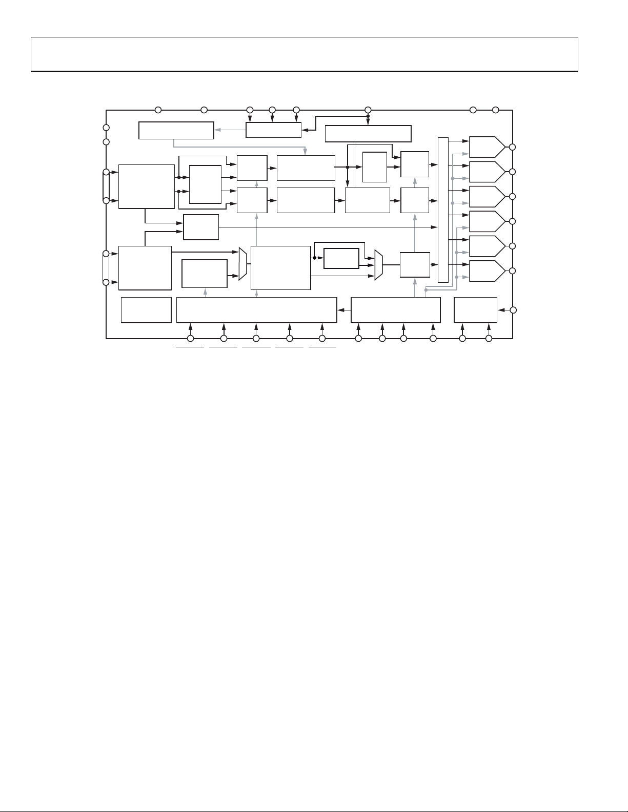
The ADV7344 is a high speed, digital-to-analog video encoder
in a 64-pin LQFP package. Six high speed, NSV, 3.3 V, 14-bit
video DACs provide support for composite (CVBS), S-Video
(YC), and component (YPrPb/RGB) analog outputs in standard
definition (SD), enhanced definition (ED), or high definition
(HD) video formats.
The ADV7344 has a 30-bit pixel input port that can be configured
in a variety of ways. SD video formats are supported over an
SDR interface and ED/HD video formats are supported over
SDR and DDR interfaces. Pixel data can be supplied in either
the YCrCb or RGB color space.
The ADV7344 also supports embedded EAV/SAV timing codes,
external video synchronization signals, and I
protocol.
In addition, simultaneous SD and ED/HD input and output is
supported. Full-drive DACs ensure that external output buffering
is not required, while 216 MHz (SD and ED) and 297 MHz
(HD) oversampling ensures that external output filtering is not
required.
Cable detection and DAC autopower-down features keep power
consumption to a minimum.
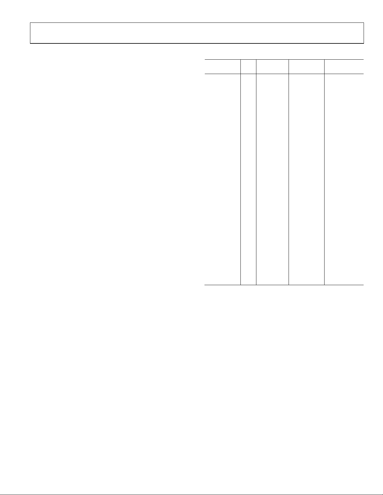
Tabl e 1 lists the video standards directly supported by the
ADV7344.
2
C® communication
Table 1. Standards Directly Supported by the ADV7344
Active
Resolution I/P
720 × 240 P 59.94 27
720 × 288 P 50 27
720 × 576 I 25 27
640 × 480 I 29.97 24.54
768 × 576 I 25 29.5
720 × 483 P 59.94 27 SMPTE 293M
720 × 483 P 59.94 27 BTA T-1004
720 × 483 P 59.94 27 ITU-R BT.1358
720 × 483 P 59.94 27 ITU-R BT.1362
720 × 576 P 50 27 ITU-R BT.1362
1920 × 1035 I 30 74.25 SMPTE 240M
1920 × 1035 I 29.97 74.1758 SMPTE 240M
1280 × 720 P
1280 × 720 P
1920 × 1080 I 30, 25 74.25 SMPTE 274M
Frame
1
Rate (Hz)
60, 50, 30,
25, 24
23.97,
59.94,
29.97
Clock Input
(MHz) Standard
ITU-R
BT.601/656
ITU-R
BT.601/656
NTSC Square
Pixel
PAL Square
Pixel
74.25 SMPTE 296M
74.1758 SMPTE 296M
1920 × 1080 P 30, 25, 24 74.25 SMPTE 274M
1920 × 1080 P
1920 × 1080 P 24 74.25 ITU-R BT.709-5
1
I = interlaced, P = progressive.
23.98,
29.97
74.1758 SMPTE 274M
Rev. B | Page 5 of 108
ADV7344 Data Sheet
R
GND_IO
V
DD_IO
8-/10-/16-/20-/
24-/30-BIT
SD
VIDEO
DATA
VIDEO
DATA
S_HSYNCP_HSYNC
P_VSYNC P_BL
ANK S_VSYNC
14-BIT
DAC 1
DAC 1
14-BIT
DAC 2
DAC 2
14-BIT
DAC 3
DAC 3
14-BIT
DAC 4
DAC 4
14-BIT
DAC 5
DAC 5
14-BIT
DAC 6
DAC 6
MULTIPLEXER
REFERENCE
AND CABLE
DETECT
16x/4x OVERSAM P LING
DAC PLL
VIDEO TIMING GENERATOR
POWER
MANAGEMENT
CONTROL
CLKIN (2) PV
DD
PGND EXT_LF (2) V
REF
COMP (2)
R
SET
(2)
SDR/DDR
ED/HD INPUT
4:2:2 TO 4:4: 4
DEINTERLEAVE
PRO
GRAMMABLE
HDTV FILTERS
SHARPNESS AND
ADAPTIVE FILTER
CONTROL
YCbCr
HDTV
TEST
PATTERN
GENERATOR
G/B
RGB
ASYNC
BYPASS
RGB
DGND (2)
V
DD
(2)
SCL SDA ALSB SFL
MPU PORT
SUBCARRIER FREQUENCY
LOCK (SFL)
YCrCb
TO
RGB
PROGRAMMABLE
CHROMINANCE
FILTER
ADD
BURST
RGB
TO
YCrCb
MATRIX
4:2:2 TO 4:4: 4
SD
DEINTERLEAVE
SIN/COS DDS
BLOCK
16×
FILTER
16×
FILTER
4×
FILTER
AGND
V
AA
ADD
SYNC
VBI DATA SERV ICE
INSERTION
PROGRAMMABLE
LUMINANCE
FILTER
06400-001
ADV7344
8-/10-/16-/20-/
24-/30-BIT
ED/HD
YCbCr
TO
RGB MATRI X
FUNCTIONAL BLOCK DIAGRAM
Figure 1.
Rev. B | Page 6 of 108

Data Sheet ADV7344
SPECIFICATIONS
POWER SUPPLY AND VOLTAGE SPECIFICATIONS
All specifications T
Table 2.
Parameter Min Typ Max Unit
SUPPLY VOLTAGES
VDD 1.71 1.8 1.89 V
V
1.71 3.3 3.63 V
DD_IO
PVDD 1.71 1.8 1.89 V
VAA 2.6 3.3 3.465 V
POWER SUPPLY REJECTION RATIO 0.002 %/%
VOLTAGE REFERENCE SPECIFICATIONS
All specifications T
Table 3.
Parameter Min Typ Max Unit
Internal Reference Range, V
External Reference Range, V
External V
1
External current required to overdrive internal V
Current1 ±10 μA
REF
MIN
MIN
to T
(−40°C to +85°C), unless otherwise noted.
MAX
to T
(−40°C to +85°C), unless otherwise noted.
MAX
1.186 1.248 1.31 V
REF
1.15 1.235 1.31 V
REF
.
REF
INPUT CLOCK SPECIFICATIONS
VDD = 1.71 V to 1.89 V, PVDD = 1.71 V to 1.89 V, VAA = 2.6 V to 3.465 V, V
All specifications T
MIN
to T
(−40°C to +85°C), unless otherwise noted.
MAX
Table 4.
Parameter Conditions1 Min Typ Max Unit
f
SD/ED 27 MHz
CLKIN_A
f
ED (at 54 MHz) 54 MHz
CLKIN_A
f
HD 74.25 MHz
CLKIN_A
f
ED 27 MHz
CLKIN_B
f
HD 74.25 MHz
CLKIN_B
CLKIN_A High Time, t9 40 % of one clock cycle
CLKIN_A Low Time, t10 40 % of one clock cycle
CLKIN_B High Time, t9 40 % of one clock cycle
CLKIN_B Low Time, t10 40 % of one clock cycle
CLKIN_A Peak-to-Peak Jitter Tolerance 2 ±ns
CLKIN_B Peak-to-Peak Jitter Tolerance 2 ±ns
1
SD = standard definition, ED = enhanced definition (525p/625p), HD = high definition.
= 1.71 V to 3.63 V.
DD_IO
Rev. B | Page 7 of 108

ADV7344 Data Sheet
ANALOG OUTPUT SPECIFICATIONS
VDD = 1.71 V to 1.89 V, PVDD = 1.71 V to 1.89 V, VAA = 2.6 V to 3.465 V, V
All specifications T
MIN
to T
(−40°C to +85°C), unless otherwise noted.
MAX
Table 5.
Parameter Conditions Min Typ Max Unit
Full Drive Output Current (Full-Scale) R
= 510 Ω, RL = 37.5 Ω 33 34.6 37 mA
SET
DAC 1, DAC 2, DAC 3 enabled1
R
= 510 Ω, RL = 37.5 Ω 33 33.5 37 mA
SET
DAC 1 enabled only2
Low-Drive Output Current (Full-Scale)3 R
= 4.12 kΩ, RL = 300 Ω 4.1 4.3 4.5 mA
SET
DAC-to-DAC Matching DAC 1 to DAC 6 1.0 %
Output Compliance, VOC 0 1.4 V
Output Capacitance, C
DAC 1, DAC 2, DAC 3 10 pF
OUT
DAC 4, DAC 5, DAC 6 6 pF
Analog Output Delay4 DAC 1, DAC 2, DAC 3 8 ns
DAC 4, DAC 5, DAC 6 6 ns
DAC Analog Output Skew DAC 1, DAC 2, DAC 3 2 ns
DAC 4, DAC 5, DAC 6 1 ns
1
Applicable to full-drive capable DACs only, that is, DAC 1, DAC 2, DAC 3.
2
The recommended method of bringing this typical value back to the ideal value is by adjusting Register 0x0B to the recommended value of 0x12.
3
Applicable to all DACs.
4
Output delay measured from the 50% point of the rising edge of the input clock to the 50% point of the DAC output full-scale transition.
= 1.71 V to 3.63 V, V
DD_IO
= 1.235 V (driven externally).
REF
DIGITAL INPUT/OUTPUT SPECIFICATIONS—3.3 V
VDD = 1.71 V to 1.89 V, PVDD = 1.71 V to 1.89 V, VAA = 2.6 V to 3.465 V, V
All specifications T
MIN
to T
(−40°C to +85°C), unless otherwise noted.
MAX
Table 6.
Parameter Conditions Min Typ Max Unit
Input High Voltage, VIH 2.0 V
Input Low Voltage, VIL 0.8 V
Input Leakage Current, IIN V
IN
= V
±10 μA
DD_IO
Input Capacitance, CIN 4 pF
Output High Voltage, VOH I
Output Low Voltage, VOL I
= 400 μA 2.4 V
SOURCE
= 3.2 mA 0.4 V
SINK
Three-State Leakage Current VIN = 0.4 V, 2.4 V ±1.0 μA
Three-State Output Capacitance 4 pF
= 2.97 V to 3.63 V.
DD_IO
DIGITAL INPUT/OUTPUT SPECIFICATIONS—1.8 V
When V
= 1.71 V to 1.89 V, PVDD = 1.71 V to 1.89 V, VAA = 2.6 V to 3.465 V, V
V
DD
All specifications T
Table 7.
Parameter Conditions Min Typ Max Unit
Input High Voltage, VIH 0.7 V
Input Low Voltage, VIL 0.3 V
Input Capacitance, CIN 4 pF
Output High Voltage, VOH I
Output Low Voltage, VOL I
Three-State Output Capacitance 4 pF
is set to 1.8 V, all the digital video inputs and control inputs, such as I2C, HS, and VS, should use 1.8 V levels.
DD_IO
= 1.71 V to 1.89 V.
DD_IO
MIN
to T
(−40°C to +85°C), unless otherwise noted.
MAX
= 400 μA V
SOURCE
= 3.2 mA 0.4 V
SINK
Rev. B | Page 8 of 108
V
DD_IO
– 0.4 V
DD_IO
V
DD_IO
Data Sheet ADV7344
ED (at 54 MHz)
1.7
ns
ED/HD-SDR or ED/HD-DDR
2.3
ns
Component Outputs (16×)
SD oversampling enabled
84 Clock cycles
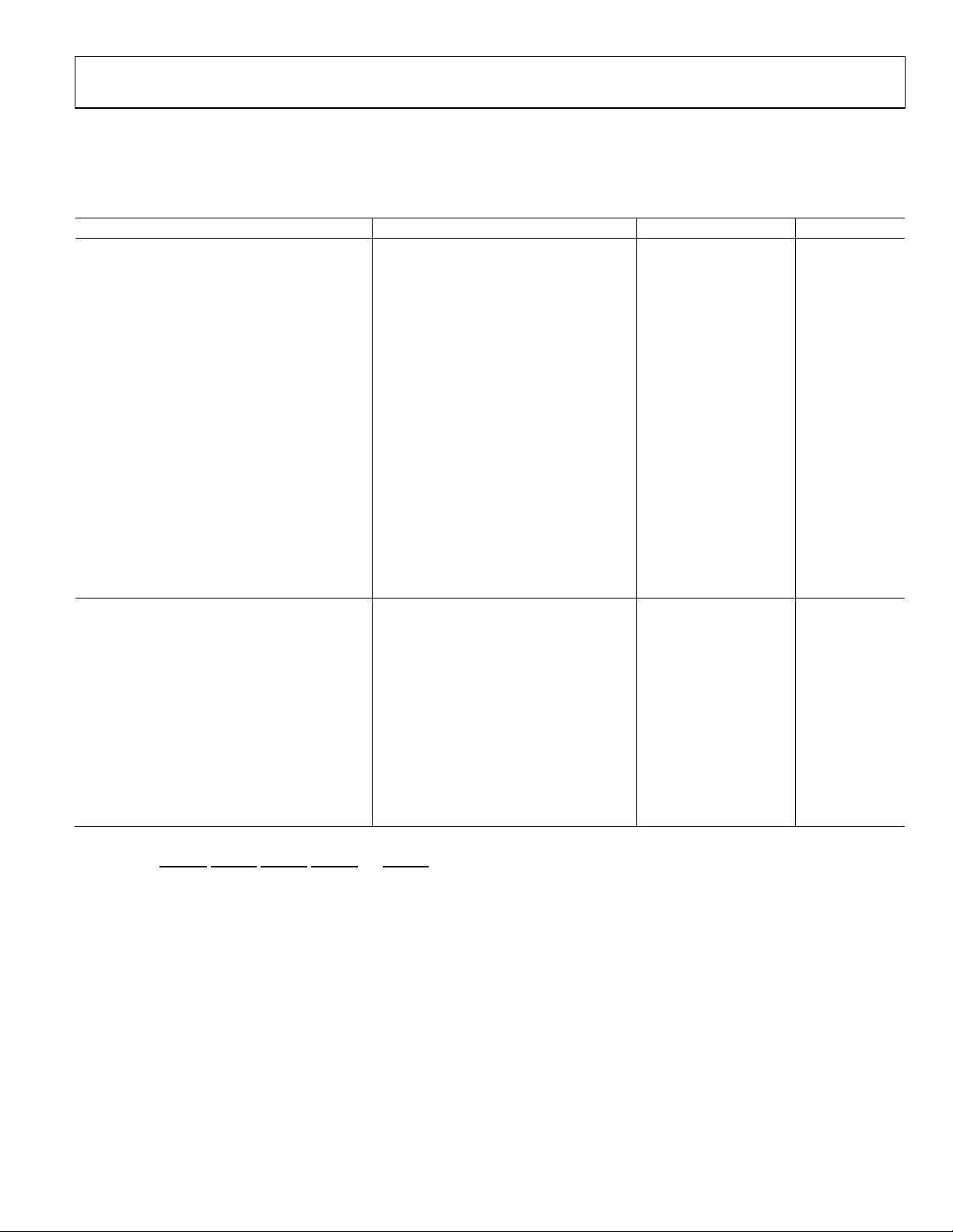
DIGITAL TIMING SPECIFICATIONS—3.3 V
VDD = 1.71 V to 1.89 V, PVDD = 1.71 V to 1.89 V, VAA = 2.6 V to 3.465 V, V
All specifications T
MIN
to T
(−40°C to +85°C), unless otherwise noted.
MAX
Table 8.
Parameter Conditions1 Min Typ Max Unit
VIDEO DATA AND VIDEO CONTROL PORT
Data Input Setup Time, t
4
SD 2.1 ns
11
2, 3
ED/HD-SDR 2.3 ns
ED/HD-DDR 2.3 ns
= 2.97 V to 3.63 V.
DD_IO
Data Input Hold Time, t
4
SD 1.0 ns
12
ED/HD-SDR 1.1 ns
ED/HD-DDR 1.1 ns
ED (at 54 MHz) 1.0 ns
Control Input Setup Time, t
4
SD 2.1 ns
11
ED (at 54 MHz) 1.7 ns
Control Input Hold Time, t
4
SD 1.0 ns
12
ED/HD-SDR or ED/HD-DDR 1.1 ns
ED (at 54 MHz) 1.0 ns
Control Output Access Time, t
4
SD 12 ns
13
ED/HD-SDR, ED/HD-DDR or ED (at 54 MHz) 10 ns
Control Output Hold Time, t
4
SD 4.0 ns
14
ED/HD-SDR, ED/HD-DDR or ED (at 54 MHz) 3.5 ns
PIPELINE DELAY5
SD1
CVBS/YC Outputs (2×) SD oversampling disabled 68 Clock cycles
CVBS/YC Outputs (16×) SD oversampling enabled 67 Clock cycles
Component Outputs (2×) SD oversampling disabled 78 Clock cycles
ED1
Component Outputs (1×) ED oversampling disabled 41 Clock cycles
Component Outputs (8×) ED oversampling enabled 46 Clock cycles
HD1
Component Outputs (1×) HD oversampling disabled 40 Clock cycles
Component Outputs (4×) HD oversampling enabled 44 Clock cycles
1
SD = standard definition, ED = enhanced definition (525p/625p), HD = high definition, SDR = single data rate, DDR = dual data rate.
2
Video data: C[9:0], Y[9:0], and S[9:0].
3
Video control:
4
Guaranteed by characterization.
5
Guaranteed by design.
P_HSYNC, P_VSYNC, P_BLANK, S_HSYNC
, and
S_VSYNC
.
Rev. B | Page 9 of 108

ADV7344 Data Sheet
ED (at 54 MHz)
1.6
ns
ED/HD-SDR or ED/HD-DDR
1.2
ns
Component Outputs (16×)
SD oversampling enabled
84 Clock cycles
DIGITAL TIMING SPECIFICATIONS—1.8 V
VDD = 1.71 V to 1.89 V, PVDD = 1.71 V to 1.89 V, VAA = 2.6 V to 3.465 V, V
All specifications T
MIN
to T
(−40°C to +85°C), unless otherwise noted.
MAX
Table 9.
Parameter Conditions1 Min Typ Max Unit
VIDEO DATA AND VIDEO CONTROL PORT
Data Input Setup Time, t
4
SD 1.4 ns
11
2, 3
ED/HD-SDR 1.9 ns
ED/HD-DDR 1.9 ns
= 1.71 V to 1.89 V.
DD_IO
Data Input Hold Time, t
4
SD 1.4 ns
12
ED/HD-SDR 1.5 ns
ED/HD-DDR 1.5 ns
ED (at 54 MHz) 1.3 ns
Control Input Setup Time, t
4
SD 1.4 ns
11
ED (at 54 MHz) 1.0 ns
Control Input Hold Time, t
4
SD 1.4 ns
12
ED/HD-SDR or ED/HD-DDR 1.0 ns
ED (at 54 MHz) 1.0 ns
Control Output Access Time, t
4
SD 13 ns
13
ED/HD-SDR, ED/HD-DDR or ED (at 54 MHz) 12 ns
Control Output Hold Time, t
4
SD 4.0 ns
14
ED/HD-SDR, ED/HD-DDR or ED (at 54 MHz) 5.0 ns
PIPELINE DELAY5
SD1
CVBS/YC Outputs (2×) SD oversampling disabled 68 Clock cycles
CVBS/YC Outputs (16×) SD oversampling enabled 67 Clock cycles
Component Outputs (2×) SD oversampling disabled 78 Clock cycles
ED1
Component Outputs (1×) ED oversampling disabled 41 Clock cycles
Component Outputs (8×) ED oversampling enabled 46 Clock cycles
HD1
Component Outputs (1×) HD oversampling disabled 40 Clock cycles
Component Outputs (4×) HD oversampling enabled 44 Clock cycles
1
SD = standard definition, ED = enhanced definition (525p/625p), HD = high definition, SDR = single data rate, DDR = dual data rate.
2
Video data: C[9:0], Y[9:0], and S[9:0].
3
Video control:
4
Guaranteed by characterization.
5
Guaranteed by design.
P_HSYNC, P_VSYNC, P_BLANK, S_HSYNC
, and
S_VSYNC
.
Rev. B | Page 10 of 108

Data Sheet ADV7344
MPU PORT TIMING SPECIFICATIONS
VDD = 1.71 V to 1.89 V, PVDD = 1.71 V to 1.89 V, VAA = 2.6 V to 3.465 V, V
All specifications T
MIN
to T
(−40°C to +85°C), unless otherwise noted.
MAX
Table 10.
Parameter Conditions Min Typ Max Unit
MPU PORT, I2C MODE1 See Figure 19
SCL Frequency 0 400 kHz
SCL High Pulse Width, t1 0.6 μs
SCL Low Pulse Width, t2 1.3 μs
Hold Time (Start Condition), t3 0.6 μs
Setup Time (Start Condition), t4 0.6 μs
Data Setup Time, t5 100 ns
SDA, SCL Rise Time, t6 300 ns
SDA, SCL Fall Time, t7 300 ns
Setup Time (Stop Condition), t8 0.6 μs
1
Guaranteed by characterization.
POWER SPECIFICATIONS
VDD = 1.8 V, PVDD = 1.8 V, VAA = 3.3 V, V
= 3.3 V, TA = 25°C.
DD_IO
= 1.71 V to 3.63 V.
DD_IO
Table 11.
Parameter Conditions Min Typ Max Unit
NORMAL POWER MODE
3
I
SD only (16× oversampling) 90 mA
DD
1, 2
ED only (8× oversampling)4 65 mA
HD only (4× oversampling)4 91 mA
SD (16× oversampling) and ED (8× oversampling) 95 mA
SD (16× oversampling) and HD (4× oversampling) 122 mA
I
1 mA
DD_IO
5
I
Three DACs enabled (ED/HD only) 124 mA
AA
Six DACs enabled (SD only and simultaneous modes ) 140 mA
I
SD only, ED only, or HD only modes 5 mA
PLL
Simultaneous modes 10 mA
SLEEP MODE
IDD 5 μA
IAA 0.3 μA
I
0.2 μA
DD_IO
I
0.1 μA
PLL
1
R
= 510 Ω (DAC 1, DAC 2 and DAC 3 operating in full-drive mode). R
SET1
2
75% color bar test pattern applied to pixel data pins.
3
IDD is the continuous current required to drive the digital core.
4
Applicable to both single data rate (SDR) and dual data rate (DDR) input modes.
5
IAA is the total current required to supply all DACs including the V
= 4.12 kΩ (DAC 4, DAC 5, and DAC 6 operating in low drive mode).
SET2
circuitry.
REF
Rev. B | Page 11 of 108

ADV7344 Data Sheet
VIDEO PERFORMANCE SPECIFICATIONS
VDD = 1.8 V, PVDD = 1.8 V, VAA = 3.3 V, V
Table 12.
Parameter Conditions Min Typ Max Unit
STATIC PERFORMANCE
Resolution 14 Bits
Integral Nonlinearity R
R
Differential Nonlinearity 1 +ve R
R
Differential Nonlinearity1 −ve R
R
STANDARD DEFINTION (SD) MODE
Luminance Nonlinearity 0.2 ±%
Differential Gain NTSC 0.2 %
Differential Phase NTSC 0.3 Degrees
SNR Luma ramp 64.5 dB
SNR Flat field full bandwidth 79.5 dB
ENHANCED DEFINITION (ED) MODE
Luma Bandwidth 12.5 MHz
Chroma Bandwidth 5.8 MHz
HIGH DEFINITION (HD) MODE
Luma Bandwidth 30 MHz
Chroma Bandwidth 13.75 MHz
1
Differential nonlinearity (DNL) measures the deviation of the actual DAC output voltage step from the ideal. For +ve DNL, the actual step value lies above the ideal
step value. For −ve DNL, the actual step value lies below the ideal step value.
= 3.3 V, TA = 25°C, V
DD_IO
= 510 Ω, RL1 = 37.5 Ω 3 LSBs
SET1
= 4.12 kΩ, R
SET2
= 510 Ω, RL1 = 37.5 Ω 1 LSBs
SET1
= 4.12 kΩ, RL2 = 300 Ω 3.2 LSBs
SET2
= 510 Ω, RL1 = 37.5 Ω 1.7 LSBs
SET1
= 4.12 kΩ, RL2 = 300 Ω 1.4 LSBs
SET2
driven externally.
REF
= 300 Ω 4 LSBs
L2
Rev. B | Page 12 of 108
Data Sheet ADV7344
TIMING DIAGRAMS
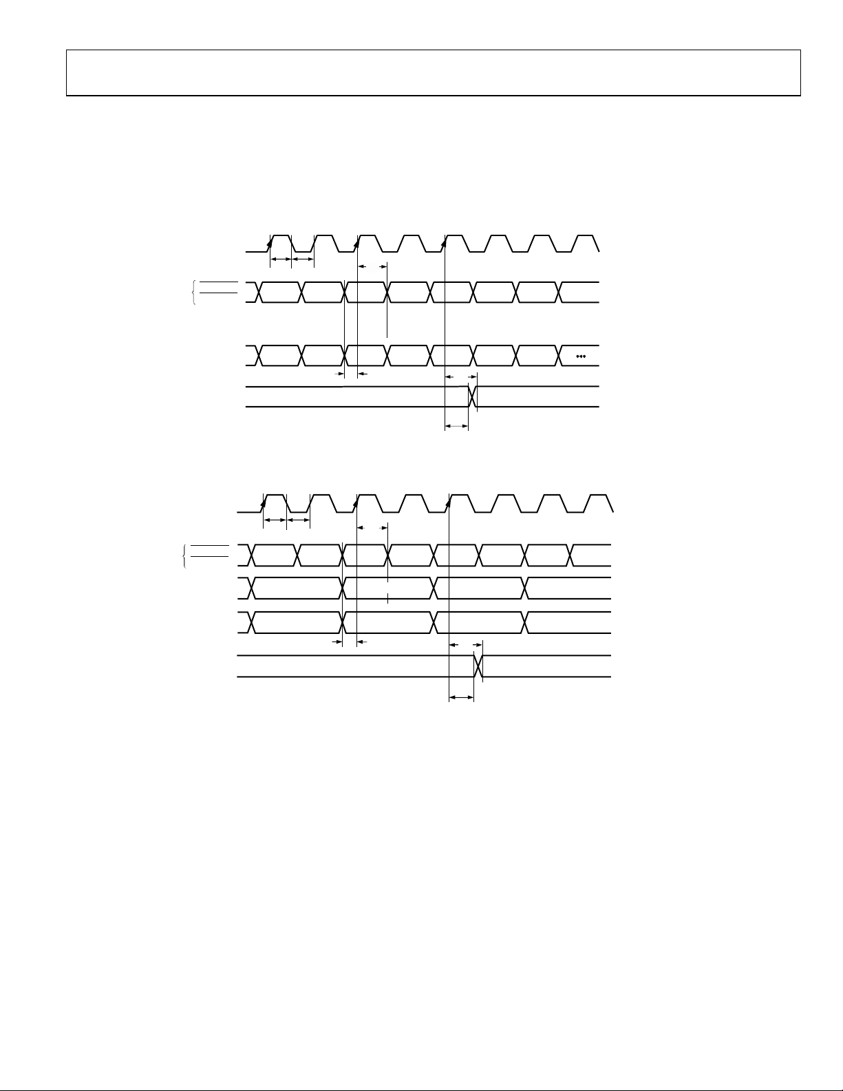
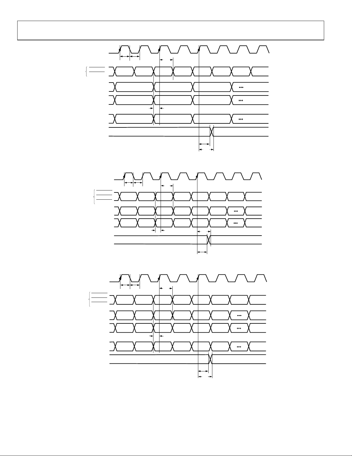
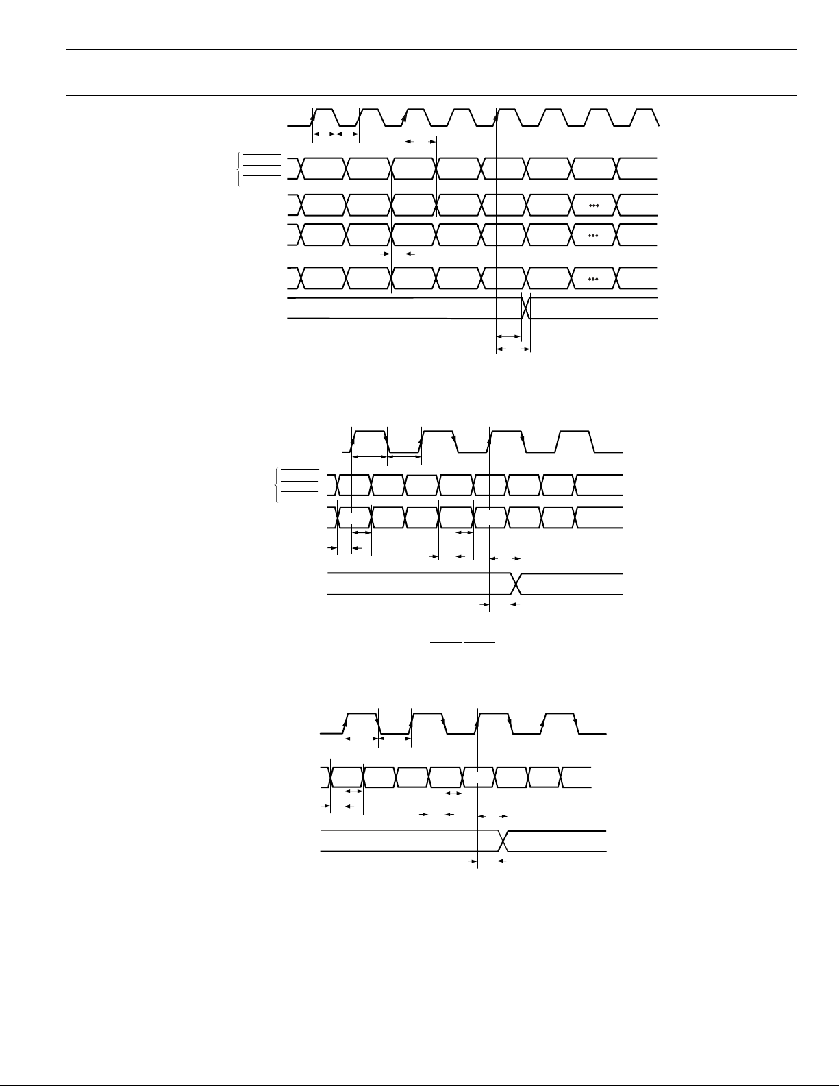
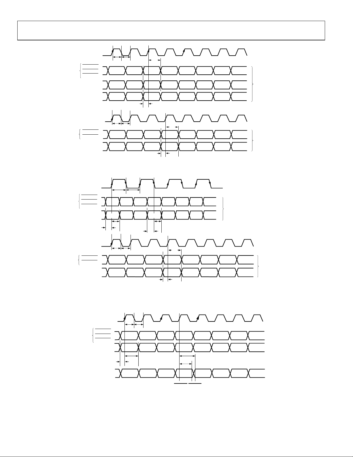
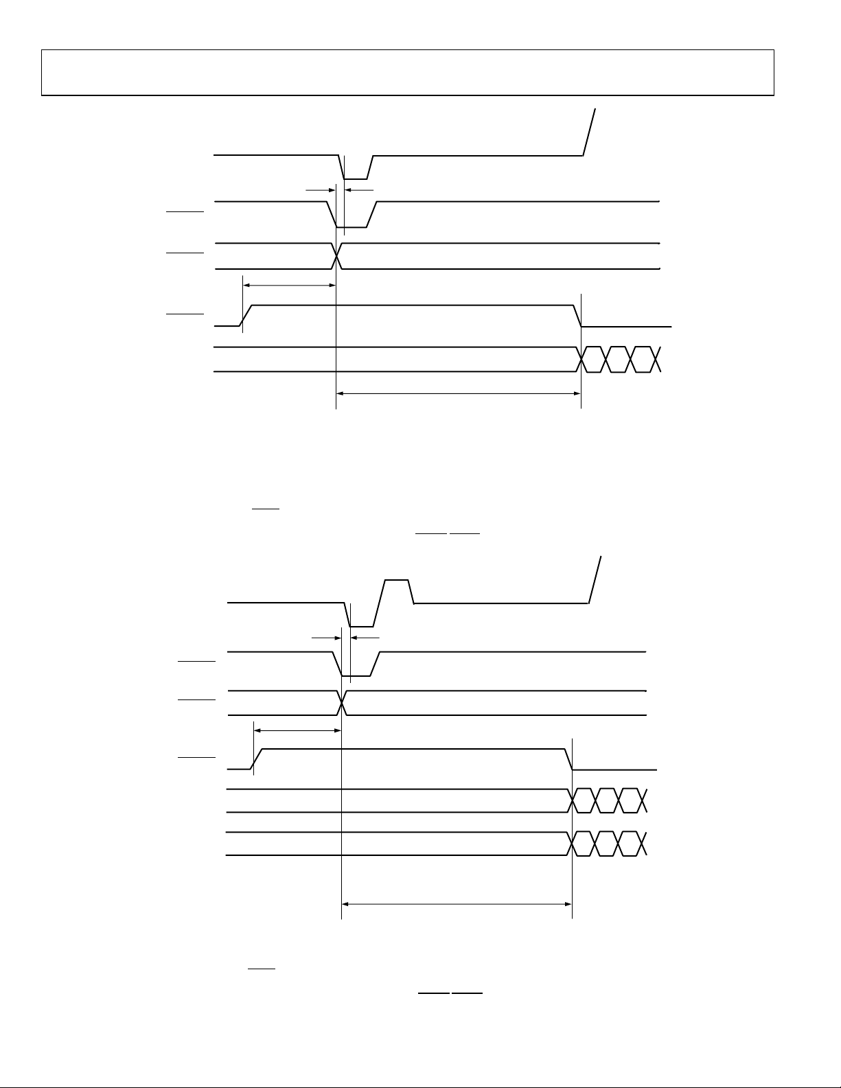
The following abbreviations are used in Figure 2 to Figure 13:
= clock high time
t
9
t
= clock low time
10
t
= data setup time
11
CLKIN_A
t
= data hold time
12
t
= control output access time
13
t
= control output hold time
14
In addition, refer to Table 36 for the ADV7344 input configuration.
t
9
CONTROL
S_HSYNC,
INPUTS
S_VSYNC
S9 TO S0/Y9 TO Y0*
CONTROL
OUTPUTS
*SELECTED BY S UBADDRES S 0x01, BIT 7.
t
10
Y0 Y1 Y2
t
11
t
12
IN SLAVE MODE
Cr2Cb2Cr0Cb0
t
13
IN MASTER/SLAVE MODE
t
14
6400-002
Figure 2. SD Only, 8-/10-Bit, 4:2:2 YCrCb Pixel Input Mode (Input Mode 000)
CLKIN_A
t9t
CONTROL
INPUTS
S_HSYNC,
S_VSYNC
S9 TO S0/Y9 TO Y0*
Y9 TO Y0/C9 TO C0*
CONTROL
OUTPUTS
*SELECT ED BY SUBADDRESS 0x01, BIT 7.
10
Y0 Y1
t
11
t
12
IN SLAVE MO DE
Y2
Cr0Cb0
Cb2
t
13
t
14
Y3
Cr2
IN MASTER/SLAVE MODE
06400-003
Figure 3. SD Only, 16-/20-Bit, 4:2:2 YCrCb Pixel Input Mode (Input Mode 000)
Rev. B | Page 13 of 108
ADV7344 Data Sheet
C9 TO C2/C9 T O C0
Y9 TO Y2/Y9 TO Y0
CONTROL
OUTPUTS
S9 TO S2/S9 TO S0
t
9
CLKIN_A
t
10
S_HSYNC,
S_VSYNC
CONTROL
INPUTS
t
11
G0 G1 G2
B0 B1 B2
R0 R1 R2
t
12
t
14
t
13
06400-004
Y0 Y1 Y2 Y3 Y4 Y5
Y9 TO Y2/Y9 TO Y0
Cr4Cb4Cr2Cb2Cr0Cb0
CONTROL
OUTPUTS
CLKIN_A
P_HSYNC,
P_VSYNC,
CONTROL
INPUTS
P_BLANK
C9 TO C2/C9 T O C0
t
9
t
10
t
12
t
11
t
14
t
13
06400-005
Y0 Y1 Y2 Y3 Y4 Y5
Cr4Cr3Cr2Cr1Cr0 Cr5
Cb4Cb3Cb
2Cb1
Cb0
Cb5
Y9 TO Y2/Y9 TO Y0
CONTROL
OUTPUTS
CLKIN_A
P_HSYNC,
P_VSYNC,
CONTROL
INPUTS
P_BLANK
C9 TO C2/C9 TO C0
S9 TO S2/S9 TO S0
t
9
t
10
t
12
t
11
t
14
t
13
06400-006
Figure 4. SD Only, 24-/30-Bit, 4:4:4 RGB Pixel Input Mode (Input Mode 000)
Figure 5. ED/HD-SDR Only, 16-/20-Bit, 4:2:2 YCrCb Pixel Input Mode (Input Mode 001)
Figure 6. ED/HD-SDR Only, 24-/30-Bit, 4:4:4 YCrCb Pixel Input Mode (Input Mode 001)
Rev. B | Page 14 of 108
Data Sheet ADV7344
CLKIN_A
C9 TO C2/C9 T O C0
G0 G1 G2 G3 G4 G5
B0 B1 B2 B3 B4 B5
R0 R1 R2 R3 R4 R5
Y9 TO Y2/Y9 TO Y0
CONTROL
OUTPUTS
S9 TO S2/S9 TO S0
P_HSYNC,
P_VSYNC,
CONTROL
INPUTS
P_BLANK
t9t
10
t
12
t
11
t
14
t
13
06400-007
CLKIN_A*
Y9 TO Y2/Y9 TO Y0
*LUMA/CHROM ACLOCK RELATIONSHIP CAN BE INVERTED
USING SUBADDRES S 0x01, BITS 1 AND 2.
CONTROL
OUTPUTS
Cr2Y2Cb2Y1Cr0Y0Cb0
t
9
t
10
t
12
t
11
t
12
t
11
t
14
t
13
P_HSYNC,
P_VSYNC,
CONTROL
INPUTS
P_BLANK
06400-008
Y1Cr0Y0Cb0XY00003FF
*LUMA/CHROM A CLOCK RELATIONSHIP CAN BE INVERTED
USING SUBADDRES S 0x01, BITS 1 AND 2.
CLKIN_A*
Y9 TO Y2/Y9 TO Y0
CONTROL
OUTPUTS
t
9
t
10
t
12
t
11
t
12
t
11
t
14
t
13
06400-009
Figure 7. ED/HD-SDR Only, 24-/30-Bit, 4:4:4 RGB Pixel Input Mode (Input Mode 001)
Figure 8. ED/HD-DDR Only, 8-/10-Bit, 4:2:2 YCrCb (
HSYNC/VSYNC
) Pixel Input Mode (Input Mode 010)
Figure 9. ED/HD-DDR Only, 8-/10-Bit, 4:2:2 YCrCb (EAV/SAV) Pixel Input Mode (Input Mode 010)
Rev. B | Page 15 of 108
ADV7344 Data Sheet
t
9
t
10
t
9
t
10
t
11
t
11
Y0
Y1
Y2
Y3
Y4
Y5
ED/HD INPUT
SD INPUT
S9 TO S2/S9 TO S0
CLKIN_A
Y2Cb2Y1Cr0Y0Cb0
Cr4Cb4Cr2Cb2Cr0Cb0
Cr2
Y6
Cb6
C9 TO C2/C9 T O C0
Y9 TO Y2/Y9 TO Y0
CLKIN_B
P_HSYNC,
P_VSYNC,
CONTROL
INPUTS
P_BLANK
S_HSYNC,
S_VSYNC
CONTROL
INPUTS
t
12
t
12
06400-010
Cr2
Cr2
Y2Y1Cr0
ED/HD INPUT
SD INPUT
Cb2Y1Cr0
S9 TO S2/S9 TO S0
CLKIN_A
Y9 TO Y2/Y9 TO Y0
CLKIN_B
P_HSYNC,
P_VSYNC,
CONTROL
INPUTS
P_BLANK
S_HSYNC,
S_VSYNC
CONTROL
INPUTS
t
9t10
t9t
10
t
12
t
11
t
12
t
11
t
12
t
11
Y0
Cb0
Cb2
Cb0 Y0 Y2
06400-011
CLKIN_A
Y9 TO Y2/Y9 TO Y0
CONTROL
OUTPUTS
Y1Cr0Y0Cb0 Cr2
Y2
Cb2
P_HSYNC,
P_VSYNC,
CONTROL
INPUTS
P_BLANK
t9t
10
t
12
t
11
t
13
t
14
06400-012
Figure 10. SD, ED/HD-SDR Input Mode, 16-/20-Bit, 4:2:2 ED/HD and 8-/10-Bit, SD Pixel Input Mode (Input Mode 011)
Figure 11. SD, ED/HD-DDR Input Mode, 8-/10-Bit, 4:2:2 ED/HD and 8-/10-Bit, SD Pixel Input Mode (Input Mode 100)
Figure 12. ED Only (at 54 MHz), 8-/10-Bit, 4:2:2 YCrCb (
HSYNC/VSYNC
) Pixel Input Mode (Input Mode 111)
Rev. B | Page 16 of 108
Data Sheet ADV7344
t
9
t
11
t
10
t
12
t
13
t
14
CLKIN_A
Y9 TO Y2/Y9 TO Y0
CONTROL
OUTPUTS
3FF 00 00 XY Cb0 Y0 Cr0 Y1
06400-013
Y0 Y1
Y2 Y3
b
a
Cr2Cb2
Cr0Cb0
c
Y OUTPUT
Y9 TO Y2/Y9 TO Y0
C9 TO C2/C9 T O C0
P_HSYNC
P_VSYNC
P_BLANK
a AND b AS PER REL E V ANT STANDARD.
c = PIPELINE DELAY. PLEASE REFER TO RELEVANT PIPELINE DELAY. THIS CAN BE FOUND IN THE DIGITAL TIMING
SPECIFICATION SECTION OF THE DATA SHEET.
A FALLING EDGE OF HSYNC INTO THE ENCODER GENERATES A SYNC FALLING EDGE ON THE OUTPUT AFTER A TIME
EQUAL TO THE PIPELINE DELAY.
06400-014
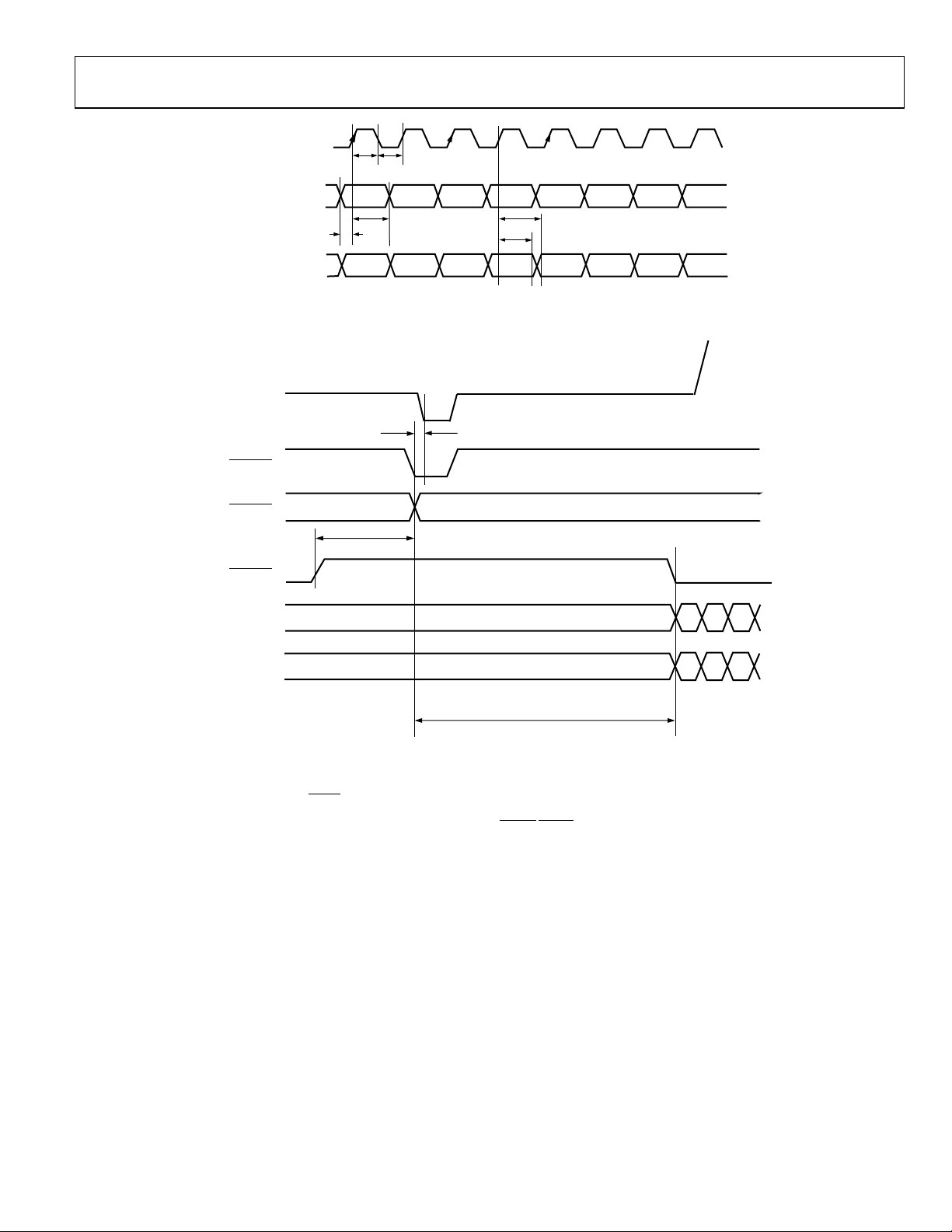
Figure 13. ED Only (at 54 MHz), 8-/10-Bit, 4:2:2 YCrCb (EAV/SAV) Pixel Input Mode (Input Mode 111)
Figure 14. ED-SDR, 16-/20-Bit, 4:2:2 YCrCb (
HSYNC/VSYNC
Rev. B | Page 17 of 108
) Input Timing Diagram
ADV7344 Data Sheet
Y9 TO Y2/Y9 TO Y0
Cb0 Y0
Cr0 Y1
b
a
a = 32 CLOCK CYCLE S FOR 525p
a = 24 CLOCK CYCLE S FOR 625p
AS RECOMMENDE D BY S TANDARD
b(MIN) = 244 CLOCK CYCLES FOR 525p
b(MIN) = 264 CLOCK CYCLES FOR 625p
P_HSYNC
P_VSYNC
P_BLANK
c
Y OUTPUT
c = PIPELINE DELAY. PLEASE REFER TO RELEVANT PIPELINE DELAY. THIS CAN BE FOUND IN THE DIGITAL TIMING
SPECIFICATION SECTION OF THE DATA SHEET.
A FALLING EDGE OF HSYNC INTO THE ENCODER GENERATES A SYNC FALLING EDGE ON THE OUTPUT AFTER A TIME
EQUAL TO THE PIPELINE DELAY.
06400-015
Y0 Y1
Y2 Y3
b
a
Cr2Cb2
Cr0Cb0
c
Y OUTPUT
Y9 TO Y2/Y9 TO Y0
C9 TO C2/C9 T O C0
P_HSYNC
P_VSYNC
P_BLANK
a AND b AS PER REL E V ANT STANDARD.
c = PIPELINE DELAY. PLEASE REFER TO RELEVANT PIPELINE DELAY. THIS CAN BE FOUND IN THE DIGITAL TIMING
SPECIFICATION SECTION OF THE DATA SHEET.
A FALLING EDGE OF HSYNC INTO THE ENCODER GENERATES A FALLING EDGE OF TRI-LEVEL SYNC ON THE OUTPUT
AFTER A TIME EQUAL TO THE PIPELINE DELAY.
06400-016
Figure 15. ED-DDR, 8-/10-Bit, 4:2:2 YCrCb (
HSYNC/VSYNC
) Input Timing Diagram
Figure 16. HD-SDR, 16-/20-Bit, 4:2:2 YCrCb (
Rev. B | Page 18 of 108
HSYNC/VSYNC
) Input Timing Diagram
Data Sheet ADV7344
Y9 TO Y2/Y9 TO Y0
Cb0 Y0
Cr0 Y1
b
a
P_HSYNC
P_VSYNC
P_BLANK
c
Y OUTPUT
a AND b AS PER REL E V ANT STANDARD.
c = PIPELINE DELAY. PLEASE REFER TO RELEVANT PIPELINE DELAY. THIS CAN BE FOUND IN THE DIGITAL TIMING
SPECIFICATION SECTION OF THE DATA SHEET.
A FALLING EDGE OF HSYNC INTO THE ENCODER GENERATES A FALLING EDGE OF TRI-LEVEL SYNC ON THE OUTPUT
AFTER A TIME EQUAL TO THE PIPELINE DELAY.
06400-017
Cb Y
Cr Y
PAL = 264 CLOCK CY CLES
NTSC = 244 CLOCK CY CLES
S9 TO S0/Y9 TO Y0*
S_VSYNC
S_HSYNC
*SELECTE D BY S UBADDRE S S 0x01, BIT 7.
06400-018
t
3
t
3
t
4
t
7
t
8
t
5
SDA
SCL
t
1
t
2
t
6
06400-019
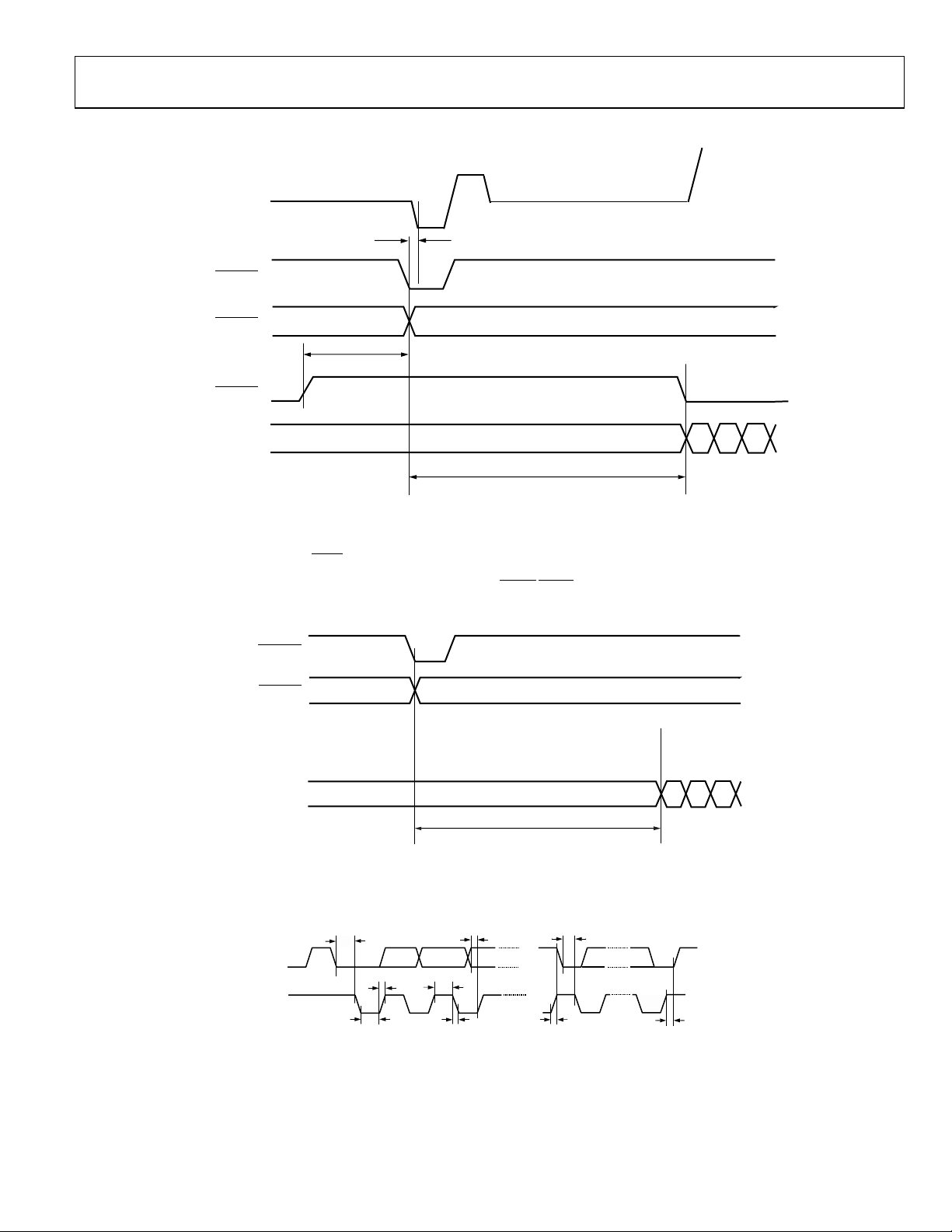
Figure 17. HD-DDR, 8-/10-Bit, 4:2:2 YCrCb (
Figure 18. SD Input Timing Diagram (Timing Mode 1)
Figure 19. MPU Port Timing Diagram (I
Rev. B | Page 19 of 108
HSYNC/VSYNC
) Input Timing Diagram
2
C Mode)
ADV7344 Data Sheet
ABSOLUTE MAXIMUM RATINGS
Table 13.
Parameter1 Rating
VAA to AGND −0.3 V to +3.9 V
VDD to DGND −0.3 V to +2.3 V
PVDD to PGND −0.3 V to +2.3 V
V
to GND_IO −0.3 V to +3.9 V
DD_IO
AGND to DGND −0.3 V to +0.3 V
AGND to PGND −0.3 V to +0.3 V
AGND to GND_IO −0.3 V to +0.3 V
DGND to PGND −0.3 V to +0.3 V
DGND to GND_IO −0.3 V to +0.3 V
PGND to GND_IO −0.3 V to +0.3 V
Digital Input Voltage to GND_IO −0.3 V to V
Analog Outputs to AGND −0.3 V to VAA
Maximum CLKIN Input Frequency 80 MHz
Storage Temperature Range (TS) −65°C to +150°C
Junction Temperature (TJ) 150°C
Lead Temperature (Soldering, 10 sec) 260°C
1
Analog output short circuit to any power supply or common can be of an
indefinite duration.
DD_IO
+ 0.3 V
Stresses above those listed under Absolute Maximum Ratings
may cause permanent damage to the device. This is a stress
rating only; functional operation of the device at these or any
other conditions above those indicated in the operational
section of this specification is not implied. Exposure to absolute
maximum rating conditions for extended periods may affect
device reliability.
The ADV7344 is a high performance integrated circuit with an
ESD rating of <1 kV, and it is ESD sensitive. Proper precautions
should be taken for handling and assembly.
THERMAL RESISTANCE
θJA is specified for the worst-case conditions, that is, a device
soldered in a circuit board for surface-mount packages.
Table 14. Thermal Resistance
Package Type θJA θ
64-Lead LQFP 47 11 °C/W
1
Values are based on a JEDEC 4-layer test board.
1
Unit
JC
The ADV7344 is an RoHS-compliant, Pb-free product. The lead
finish is 100% pure Sn electroplate. The device is suitable for Pbfree applications up to 255°C (±5°C) IR reflow (JEDEC STD-20).
It is backward compatible with conventional SnPb soldering
processes. The electroplated Sn coating can be soldered with
Sn/Pb solder paste at conventional reflow temperatures of
220°C to 235°C.
ESD CAUTION
Rev. B | Page 20 of 108
Data Sheet ADV7344
S_HSYNC49S_VSYNC
V
Y7
10
V
DD
12
Y8
13
Y9
14
C0
15
C1
16
C2
11
DGND
17C318C419
ALSB
20
SDA
21
SCL
22 23
P_HSYNC
24
P_VSYNC
25
P_BLANK
26
C6
C527C728C829C9
30
CLKIN_A
31 32
PGND
PIN 1
ADV7344
TOP VIEW
(Not to S cale)
EXT_LF2
06400-021
PIN CONFIGURATION AND FUNCTION DESCRIPTIONS
DD
55S454S353S252S151S050
48
47
46
45
44
43
42
41
40
39
38
37
36
35
34
33
SFL
R
SET1
V
REF
COMP1
DAC 1
DAC 2
DAC 3
V
AA
AGND
DAC 4
DAC 5
DAC 6
R
SET2
COMP2
PV
DD
EXT_LF1
DD_IO
GND_IO63CLKIN_B62S961S860S759S658S557DGND56V
64
1
2
Y0
3
Y1
4
Y2
5
Y3
6
Y4
7
Y5
8
Y6
9
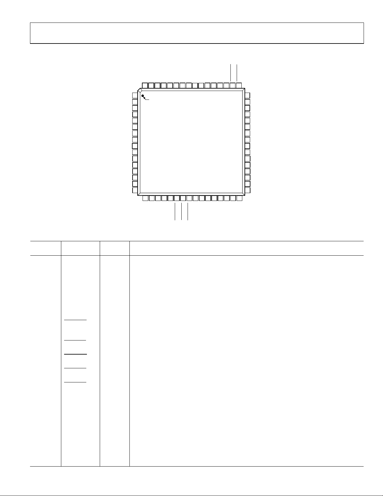
Figure 20. Pin Configuration
Table 15. Pin Function Descriptions
Input/
Pin No. Mnemonic
13, 12,
Y9 to Y0 I 10-Bit Pixel Port (Y9 to Y0). Y0 is the LSB. Refer to Table 36 for input modes.
Output Description
9 to 2
29 to 25,
C9 to C0 I 10-Bit Pixel Port (C9 to C0). C0 is the LSB. Refer to Table 36 for input modes.
18 to 14
62 to 58,
S9 to S0 I 10-Bit Pixel Port (S9 to S0). S0 is the LSB. Refer to Table 36 for input modes.
55 to 51
30 CLKIN_A I Pixel Clock Input for HD only (74.25 MHz), ED1 only (27 MHz or 54 MHz), or SD only (27 MHz).
63 CLKIN_B I
Pixel Clock Input for Dual Modes Only. Requires a 27 MHz reference clock for ED operation or a
74.25 MHz reference clock for HD operation.
50
S_HSYNC
I/O
SD Horizontal Synchronization Signal. This pin can also be configured to output an SD, ED, or HD
horizontal synchronization signal. See the External Horizontal and Vertical Synchronization
Control section.
49
22
S_VSYNC
P_HSYNC
I/O
I
SD Vertical Synchronization Signal. This pin can also be configured to output an SD, ED, or HD vertical
synchronization signal. See the External Horizontal and Vertical Synchronization Control section.
ED/HD Horizontal Synchronization Signal. See the External Horizontal and Vertical Synchronization
Control section.
23
24
P_VSYNC
P_BLANK
I
ED/HD Vertical Synchronization Signal. See the External Horizontal and Vertical Synchronization
Control section.
I ED/HD Blanking Signal. See the External Horizontal and Vertical Synchronization Control section.
48 SFL I/O Subcarrier Frequency Lock (SFL) Input.
47 R
36 R
45, 35
44, 43, 42
I
SET1
I
SET2
COMP1,
COMP2
DAC 1, DAC 2,
DAC 3
O Compensation Pins. Connect a 2.2 nF capacitor from both COMP pins to V
O DAC Outputs. Full- and low -drive capable DACs.
This pin is used to control the amplitudes of the DAC 1, DAC 2, and DAC 3 outputs. For full-drive
operation (for example, into a 37.5 Ω load), a 510 Ω resistor must be connected from R
SET1
to
AGND. For low-drive operation (for example, into a 300 Ω load), a 4.12 kΩ resistor must be
connected from R
to AGND.
SET1
This pin is used to control the amplitudes of the DAC 4, DAC 5, and DAC 6 outputs. A 4.12 kΩ
resistor must be connected from R
Rev. B | Page 21 of 108
to AGND.
SET2
.
AA

ADV7344 Data Sheet
10, 56
VDD
P
Digital Power Supply (1.8 V). For dual-supply configurations, VDD can be connected to other 1.8 V
31
EXT_LF2
I
External Loop Filter for On-Chip PLL 2.
Input/
Pin No. Mnemonic
39, 38, 37
DAC 4, DAC 5,
DAC 6
21 SCL I I2C Clock Input.
20 SDA I/O I2C Data Input/Output.
19 ALSB I
46 V
Optional External Voltage Reference Input for DACs or Voltage Reference Output.
REF
41 VAA P Analog Power Supply (3.3 V).
1 V
P Input/Output Digital Power Supply (1.8 V or 3.3 V).
DD_IO
34 PVDD P
33 EXT_LF1 I External Loop Filter for On-Chip PLL 1.
32 PGND G PLL Ground Pin.
40 AGND G Analog Ground Pin.
11, 57 DGND G Digital Ground Pin.
64 GND_IO G Input/Output Supply Ground Pin.
1
ED = enhanced definition = 525p and 625p.
2
LSB = least significant bit. In the ADV7344, setting the LSB to 0 sets the I2C address to 0xD4. Setting it to 1 sets the I2C address to 0xD6.
Output Description
O DAC Outputs. Low-drive only capable DACs.
2
This signal sets up the LSB
of the MPU I2C address (see the Power Supply Sequencing section for
more information).
supplies through a ferrite bead or suitable filtering.
PLL Power Supply (1.8 V). For dual-supply configurations, PV
supplies through a ferrite bead or suitable filtering.
can be connected to other 1.8 V
DD
Rev. B | Page 22 of 108

Data Sheet ADV7344
FREQUENCY (MHz)
EDPr/Pb RESPONSE. LINEAR INTERP FROM 4:2:2 TO 4:4:4
0
GAIN (dB)
–70
–60
–50
–40
–30
–20
–10
–80
20020 40 60 80 100 120 140 160 1800
06400-022
FREQUENCY (MHz)
EDPr/Pb RESPONSE. SSAF INTERP FROM 4:2:2 TO 4:4:4
0
GAIN (dB)
–70
–60
–50
–40
–30
–20
–10
–80
20020 40 60 80 100 120 140 160 1800
06400-023
FREQUENCY (MHz)
Y RESPONSE IN ED 8× OVERSAMPLING MODE
0
GAIN (dB)
–70
–60
–50
–40
–30
–20
–10
–80
200
20 40 60 80 100 120 140 160 1800
06400-024
FREQUENCY (MHz)
Y RESPONSE IN ED 8× OVERSAMPLING MODE
GAIN (dB)
–2.5
–2.0
–1.5
–1.0
–0.5
0
0.5
1.0
–3.0
122 4 6 8 100
06400-025
FREQUENCY (MHz)
HD Pr/Pb RESPONSE. SSAF INTERP FROM 4:2:2 TO 4:4:4
10
0
GAIN (dB)
–70
–60
–50
–40
–30
–20
–10
–100
–80
–90
148.018.
5 37.0 55.5 74.0 92.5 111.0 129.50
06400-026
HD Pr/Pb RES P ONSE. 4:4:4 I NP UT MODE
GAIN (dB)
FREQUENCY (MHz)
0
–10
–20
–30
–40
–50
–60
–70
–80
–90
–100
10 20 30 40 50 60 70 80 90 100 110 120 130 140
06400-027
TYPICAL PERFORMANCE CHARACTERISTICS
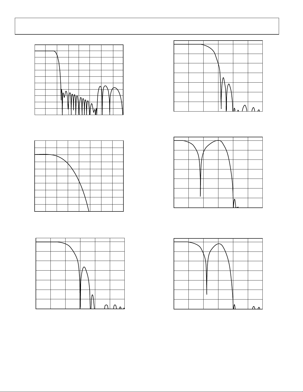
Figure 21. ED 8× Oversampling, PrPb Filter (Linear) Response
Figure 22. ED 8× Oversampling, PrPb Filter (SSAF™) Response
Figure 24. ED 8× Oversampling, Y Filter Response (Focus on Pass Band)
Figure 25. HD 4× Oversampling, PrPb (SSAF) Filter Response (4:2:2 Input)
Figure 23. ED 8× Oversampling, Y Filter Response
Figure 26. HD 4× Oversampling, PrPb (SSAF) Filter Response (4:4:4 Input)
Rev. B | Page 23 of 108
ADV7344 Data Sheet
FREQUENCY (MHz)
Y RESPONSE IN HD 4× OVERSAMPLING MODE
10
0
GAIN (dB)
–70
–60
–50
–40
–30
–20
–10
–100
–80
–90
148.018.5 37.0 55.5 74.0 92.5 111.0 129.50
06400-028
Y PASS BAND IN HD 4x O V E RS AM P LING MODE
3.0
–12.0
27.750 46.250
FREQUENCY (MHz)
GAIN (dB)
1.5
0
–1.5
–3.0
–4.5
–6.0
–7.
5
–9.0
–10.5
30.063 32.375 34.688 37.000 39.312 41.625 43.937
06400-029
FREQUENCY (MHz)
MAGNITUDE ( dB)
0
121086420
–10
–30
–50
–60
–70
–20
–40
06400-030
FREQUENCY (MHz)
MAGNITUDE ( dB)
0
121086420
–10
–30
–50
–60
–70
–20
–40
06400-031
FREQUENCY (MHz)
MAGNITUDE ( dB)
0
121086420
–10
–30
–50
–60
–70
–20
–40
06400-032
FREQUENCY (MHz)
MAGNITUDE ( dB)
0
121086
420
–10
–30
–50
–60
–70
–20
–40
06400-033
Figure 27. HD 4× Oversampling, Y Filter Response
Figure 28. HD 4× Oversampling, Y Filter Response (Focus on Pass Band)
Figure 30. SD PAL, Luma Low-Pass Filter Response
Figure 31. SD NTSC, Luma Notch Filter Response
Figure 29. SD NTSC, Luma Low-Pass Filter Response
Figure 32. SD PAL, Luma Notch Filter Response
Rev. B | Page 24 of 108

Data Sheet ADV7344
FREQUENCY (MHz)
Y RESPONSE IN SD O VERSA MPL I NG MO D E
GAIN (dB)
0
–50
–80
0 20 40 60 80 100 120 140 160 180 200
–10
–40
–60
–70
–20
–30
06400-034
FREQUENCY (MHz)
MAGNITUDE ( dB)
0
121086420
–10
–30
–50
–60
–70
–20
–40
06400-035
FREQUENCY (MHz)
4
7
MAGNITUDE ( dB)
2
–2
–6
–8
–12
0
–4
5
–10
6
0
1
2
3
4
06400-036
FREQUENCY (MHz)
7
MAGNITUDE ( dB)
5
4
2
1
–1
3
5
0
6
0
1
2
3
4
06400-037
FREQUENCY (MHz)
7
MAGNITUDE ( dB)
1
0
–2
–3
–5
–1
5
–4
6
0
1
2
3
4
06400-038
FREQUENCY (MHz)
0
12
MAGNITUDE ( dB)
–10
–30
–50
–60
–70
–20
–40
10
8
4
620
06400-039
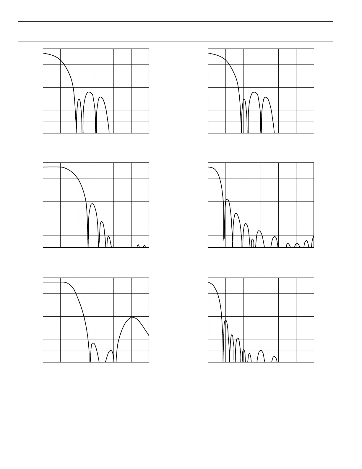
Figure 33. SD, 16× Oversampling, Y Filter Response
Figure 34. SD Luma SSAF Filter Response up to 12 MHz
Figure 36. SD Luma SSAF Filter, Programmable Gain
Figure 37. SD Luma SSAF Filter, Programmable Attenuation
Figure 35. SD Luma SSAF Filter, Programmable Responses
Figure 38. SD Luma CIF Low-Pass Filter Response
Rev. B | Page 25 of 108
ADV7344 Data Sheet
FREQUENCY (MHz)
0
12
MAGNITUDE ( dB)
–10
–30
–50
–60
–70
–20
–40
10
8
4
620
06400-040
FREQUENCY (MHz)
0
12
MAGNITUDE ( dB)
–10
–30
–50
–60
–70
–20
–40
10
8
4
620
06400-041
FREQUENCY (MHz)
0
12
MAGNITUDE ( dB)
–10
–30
–50
–60
–70
–20
–40
10
8
4
620
06400-042
FREQUENCY (MHz)
0
12
MAGNITUDE ( dB)
–10
–30
–50
–60
–70
–20
–40
10
8
4
620
06400-043
FREQUENCY (MHz)
0
12
MAGNITUDE ( dB)
–10
–30
–50
–60
–70
–20
–40
10
8
4
620
06400-044
FREQUENCY (MHz)
0
12
MAGNITUDE ( dB)
–10
–30
–50
–60
–70
–20
–40
10
8
4
620
06400-045
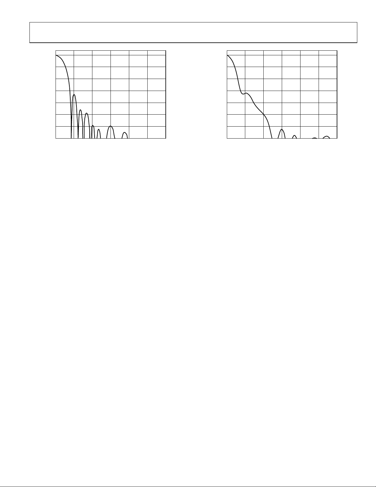
Figure 39. SD Luma QCIF Low-Pass Filter Response
Figure 40. SD Chroma 3.0 MHz Low-Pass Filter Response
Figure 42. SD Chroma 1.3 MHz Low-Pass Filter Response
Figure 43. SD Chroma 1.0 MHz Low-Pass Filter Response
Figure 41. SD Chroma 2.0 MHz Low-Pass Filter Response
Figure 44. SD Chroma 0.65 MHz Low-Pass Filter Response
Rev. B | Page 26 of 108
Data Sheet ADV7344
FREQUENCY (MHz)
0
12
MAGNITUDE ( dB)
–10
–30
–50
–60
–70
–20
–40
10
8
4
620
06400-046
FREQUENCY (MHz)
0
12
MAGNITUDE ( dB)
–10
–30
–50
–60
–70
–20
–40
10
8
4
620
06400-047
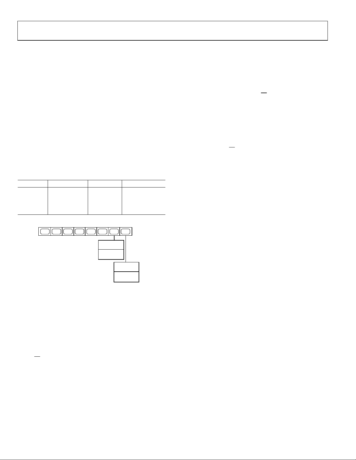
Figure 45. SD Chroma CIF Low-Pass Filter Response
Figure 46. SD Chroma QCIF Low-Pass Filter Response
Rev. B | Page 27 of 108
ADV7344 Data Sheet
1 1 0
1 0
1 A1 X
ADDRESS
CONTROL
SET UP BY
ALSB
READ/WRITE
CONTROL
0 WRITE
1 READ
06400-048
MPU PORT DESCRIPTION
Devices such as a microprocessor can communicate with the
ADV7344 through a 2-wire serial l(I
power-up or reset, the MPU port is configured for I
2
C-compatible) bus. After
2
C operation.
I2C OPERATION
The ADV7344 supports a 2-wire serial (I2C-compatible)
microprocessor bus driving multiple peripherals. This port
operates in an open-drain configuration. Two wires, serial data
(SDA) and serial clock (SCL), carry information between any
device connected to the bus and the ADV7344. The slave
address of the ADV7344 depends on the operation (read or
write) and the state of the ALSB pin (0 or 1). See Ta b l e 16 and
Figure 47. The LSB sets either a read or a write operation. Logic 1
corresponds to a read operation, and Logic 0 corresponds to a
write operation. A1 is controlled by setting the ALSB pin of the
ADV7344 to Logic 0 or Logic 1.
Table 16. ADV7344 I
Device ALSB Operation Slave Address
ADV7344 0 Write 0xD4
0 Read 0xD5
1 Write 0xD6
1 Read 0xD7
Analog Devices, Inc., strongly recommends tying ALSB to
V
. If this is not done, a power supply sequence (PSS) may be
DD_IO
required. For more information on the PSS, see the Power Supply
Sequencing section. The various devices on the bus use the
following protocol. The master initiates a data transfer by
establishing a start condition, defined by a high-to-low
transition on SDA while SCL remains high. This indicates that
an address/data stream follows. All peripherals respond to the
start condition and shift the next eight bits (7-bit address plus
W
the R/
bit).The bits are transferred from MSB down to LSB.
The peripheral that recognizes the transmitted address
2
C Slave Addresses
Figure 47. ADV7344 I
2
C Slave Address
responds by pulling the data line low during the ninth clock
pulse. This is known as an acknowledge bit. All other devices
withdraw from the bus at this point and maintain an idle
condition. The idle condition occurs when the device monitors
the SDA and SCL lines waiting for the start condition and the
correct transmitted address. The R/
W
bit determines the
direction of the data.
Logic 0 on the LSB of the first byte means that the master writes
information to the peripheral. Logic 1 on the LSB of the first byte
means that the master reads information from the peripheral.
The ADV7344 acts as a standard slave device on the bus. The
data on the SDA pin is eight bits long, supporting the 7-bit
addresses plus the R/
W
bit. It interprets the first byte as the
device address and the second byte as the starting subaddress.
There is a subaddress auto-increment facility. This allows data
to be written to or read from registers in ascending subaddress
sequence starting at any valid subaddress. A data transfer is
always terminated by a stop condition. The user can also access
any unique subaddress register on a one-by-one basis without
updating all the registers.
Stop and start conditions can be detected at any stage during
the data transfer. If these conditions are asserted out of
sequence with normal read and write operations, they cause an
immediate jump to the idle condition. During a given SCL high
period, the user should issue only a start condition, a stop
condition, or a stop condition followed by a start condition. If
an invalid subaddress is issued by the user, the ADV7344 does
not issue an acknowledge but returns to the idle condition. If
the user uses the auto-increment method of addressing the
encoder and exceeds the highest subaddress, the following
actions are taken:
• In read mode, the highest subaddress register contents are
output until the master device issues a no acknowledge.
This indicates the end of a read. A no acknowledge
condition occurs when the SDA line is not pulled low on
the ninth pulse.
• In write mode, the data for the invalid byte is not loaded
into any subaddress register, a no acknowledge is issued by
the ADV7344, and the part returns to the idle condition.
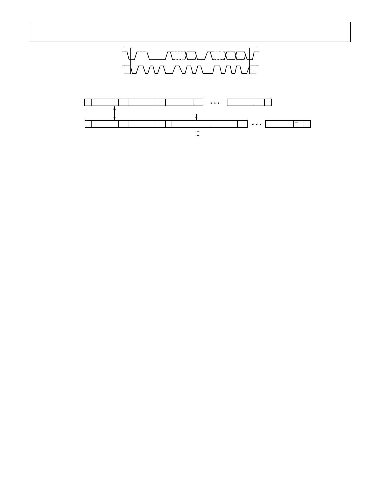
Figure 48 shows an example of data transfer for a write sequence
and the start and stop conditions. Figure 49 shows bus write and
read sequences.
Rev. B | Page 28 of 108
Data Sheet ADV7344
SDA
SCL
START ADDR R/W ACK SUBADDRESS ACK DATA ACK STOP
1–7 8
9S1–7
1–7
P
8
9
8
9
06400-049
WRITE
SEQUENCE
READ
SEQUENCE
S SL AV E ADDR A(S) SUBADDR A(S) DATA DATA A(S) P
S SL AV E ADDR A(S) SUBADDR A(S) S SL AV E ADDR A(S) DATA DATAA(M) A(M) P
S = START BI T
P = STOP BIT
A(S) = ACKNOWLEDGE BY SL AV E
A(M) = ACKNOWLEDGE BY MASTER
A(S) = NO-ACKNOWLEDGE BY SLAVE
A(M) = NO-ACKNOWLEDGE BY MASTER
LSB = 0
LSB = 1
A(S)
06400-050
Figure 48. I
2
C Data Transfer
Figure 49. I
2
C Read and Write Sequence
Rev. B | Page 29 of 108
ADV7344 Data Sheet
REGISTER MAP ACCESS
A microprocessor can read from or write to all registers of the
ADV7344 via the MPU port, except for registers that are specified
as read-only or write-only registers.
The subaddress register determines which register the next
read or write operation accesses. All communication through
the MPU port starts with an access to the subaddress register.
A read/write operation is then performed from/to the target
address, which increments to the next address until the
transaction is complete.
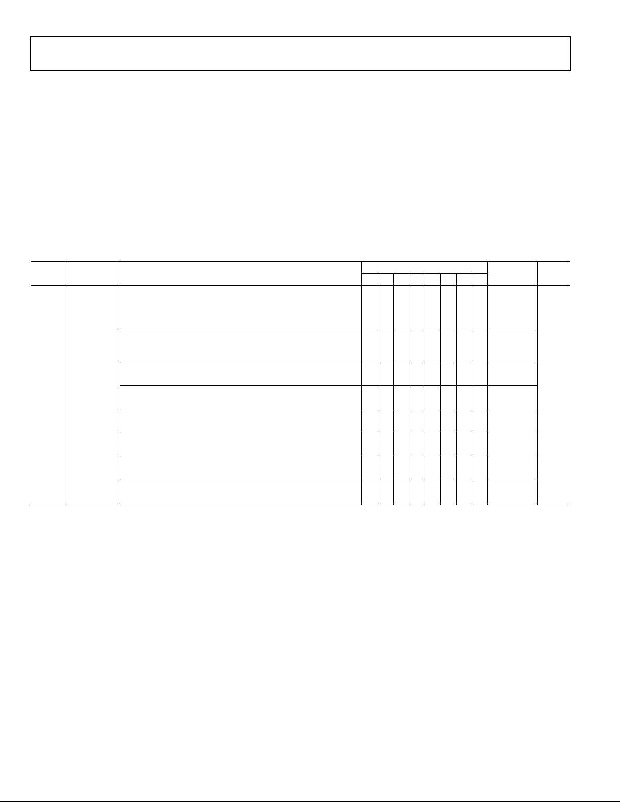
Table 17. Register 0x00
SR7 to Bit Number Register Reset
SR0 Register Bit Description 7 6 5 4 3 2 1 0 Setting Value
0x00 Power
mode
Sleep mode. With this control enabled, the current consumption
is reduced to µA level. All DACs and the internal PLL circuits are
disabled. Registers can be read from and written to in sleep
mode.
PLL and oversampling control. This control allows the internal
PLL 1 circuit to be powered down and the oversampling to be
switched off.
DAC 3: power on/off. 0 DAC 3 off
DAC 2: power on/off. 0 DAC 2 off
DAC 1: power on/off. 0 DAC 1 off
DAC 6: power on/off. 0 DAC 6 off
DAC 5: power on/off. 0 DAC 5 off
DAC 4: power on/off. 0 DAC 4 off
REGISTER PROGRAMMING
Tabl e 17 to Tabl e 35 describe the functionality of each register.
All registers can be read from as well as written to, unless
otherwise stated.
SUBADDRESS REGISTER (SR7 TO SR0)
The subaddress register is an 8-bit write-only register. After the
MPU port is accessed and a read/write operation is selected, the
subaddress is set up. The subaddress register determines to or
from which register the operation takes place.
0 Sleep
mode off
1 Sleep
mode on
0 PLL 1 on
1 PLL 1 off
1 DAC 3 on
1 DAC 2 on
1 DAC 1 on
1 DAC 6 on
1 DAC 5 on
1 DAC 4 on
0x12
Rev. B | Page 30 of 108
 Loading...