Multiformat 216 MHz
Video Encoder with Six NSV
™
14-Bit DACs
ADV7314
FEATURES
High Definition Input Formats
8-/10-,16-/20-, 24-/30-Bit (4:2:2, 4:4:4) Parallel YCrCb
Compliant with:
SMPTE 293M (525p)
BTA T-1004 EDTV2 525p
ITU-R BT.1358 (625p/525p)
ITU-R BT.1362 (625p/525p)
SMPTE 274M (1080i) at 30 Hz and 25 Hz
SMPTE 296M (720p)
RGB in 3 10-Bit 4:4:4 Input Format
HDTV RGB Supported:
RGB and RGBHV
Other High Definition Formats Using Async
Timing Mode
High Definition Output Formats
YPrPb Progressive Scan (EIA-770.1, EIA-770.2)
YPrPb HDTV (EIA 770.3)
RGB, RGBHV
CGMS-A (720p/1080i)
Macrovision Rev 1.1 (525p/625p)
CGMS-A (525p)
Standard Definition Input Formats
CCIR-656 4:2:2 8-/10-/16-/20-Bit Parallel Input
Standard Definition Output Formats
Composite NTSC M/N
Composite PAL M/N/B/D/G/H/I, PAL-60
SMPTE 170M NTSC Compatible Composite Video
ITU-R BT.470 PAL Compatible Composite Video
S-Video (Y/C)
EuroScart RGB
Component YPrPb (Betacam, MII, SMPTE/EBU N10)
Macrovision Rev 7.1.L1
CGMS/WSS
Closed Captioning
GENERAL FEATURES
Simultaneous SD and HD Inputs and Outputs
Oversampling up to 216 MHz
Programmable DAC Gain Control
Sync Outputs in All Modes
Purchase of licensed I2C components of Analog Devices or one of its
sublicensed Associated Companies conveys a license for the purchaser under
the Philips I2C Patent Rights to use these components in an I2C system,
provided that the system conforms to the I2C Standard Specification as
defined by Philips.
On-Board Voltage Reference
Six 14-Bit NSV Precision Video DACs
2-Wire Serial I
2C®
Interface
Dual Input/Output Supply 2.5 V/3.3 V Operation
Analog and Digital Supply 2.5 V
On-Board PLL
64-Lead LQFP Package
Lead (Pb) Free Product
APPLICATIONS
High End DVD
High End PS DVD Recorders/Players
SD/Prog Scan/HDTV Display Devices
SD/HDTV Set Top Boxes
Professional Video Systems
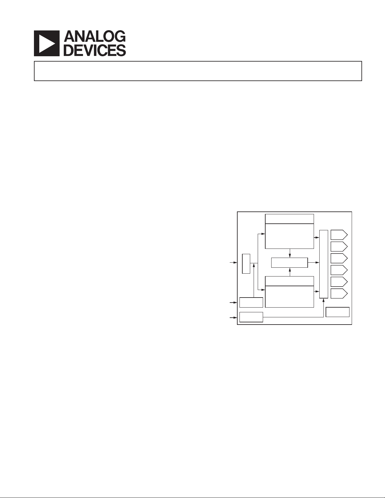
SIMPLIFIED FUNCTIONAL BLOCK DIAGRAM
STANDARD DEFINITION
CONTROL BLOCK
COLOR CONTROL
BRIGHTNESS
DNR
GAMMA
PROGRAMMABLE FILTERS
SD TEST PATTERN
PROGRAMMABLE
RGB MATRIX
HIGH DEFINITION
CONTROL BLOCK
HD TEST PATTERN
COLOR CONTROL
ADAPTIVE FILTER CTRL
SHARPNESS FILTER
O
V
E
R
S
A
M
P
L
I
N
G
INTERFACE
14-BIT
DAC
14-BIT
DAC
14-BIT
DAC
14-BIT
DAC
14-BIT
DAC
14-BIT
DAC
I2C
Y9–Y0
C9–C0
S9–S0
HSYNC
VSYNC
BLANK
CLKIN_A
CLKIN_B
ADV7314
D
E
M
U
X
TIMING
GENERATOR
PLL
GENERAL DESCRIPTION
The ADV®7314 is a high speed, digital-to-analog encoder on a
single monolithic chip. It includes six high speed NSV video
D/A converters with TTL compatible inputs.
The ADV7314 has separate 8-/10-/16-/20-bit input ports that
accept data in high definition and/or standard definition video
format. For all standards, external horizontal, vertical and
blanking signals, or EAV/SAV timing codes control the insertion of appropriate synchronization signals into the digital data
stream and therefore the output signal.
REV. 0
Information furnished by Analog Devices is believed to be accurate and
reliable. However, no responsibility is assumed by Analog Devices for its
use, nor for any infringements of patents or other rights of third parties that
may result from its use. No license is granted by implication or otherwise
under any patent or patent rights of Analog Devices. Trademarks and
registered trademarks are the property of their respective companies.
One Technology Way, P.O. Box 9106, Norwood, MA 02062-9106, U.S.A.
Tel: 781/329-4700 www.analog.com
Fax: 781/326-8703 © 2003 Analog Devices, Inc. All rights reserved.
ADV7314
P
P
P
DETAILED FEATURES
High Definition Programmable Features (720p/1080i)
2 Oversampling (148.5 MHz)
Internal Test Pattern Generator
(Color Hatch, Black Bar, Flat Field/Frame)
Fully Programmable YCrCb to RGB Matrix
Gamma Correction
Programmable Adaptive Filter Control
Programmable Sharpness Filter Control
CGMS-A (720p/1080i)
Programmable Features (525p/625p)
8 Oversampling (216 MHz Output)
Internal Test Pattern Generator
(Color Hatch, Black Bar, Flat Frame)
Individual Y and PrPb Output Delay
Gamma Correction
Programmable Adaptive Filter Control
Fully Programmable YCrCb to RGB Matrix
Undershoot Limiter
Macrovision Rev 1.1 (525p/625p)
CGMS-A (525p)
Standard Definition Programmable Features
16 Oversampling (216 MHz)
Internal Test Pattern Generator (Color Bars, Black Bar)
Controlled Edge Rates for Sync, Active Video
Individual Y and PrPb Output Delay
Gamma Correction
Digital Noise Reduction (DNR)
Multiple Chroma and Luma Filters
Luma-SSAF™ Filter with Programmable
Gain/Attenuation
PrPb SSAF
Separate Pedestal Control on Component and
Composite/S-Video Outputs
VCR FF/RW Sync Mode
Macrovision Rev 7.1.L1
CGMS/WSS
Closed Captioning
Standards Directly Supported
Frame Rate Clk Input
Resolution (Hz) (MHz) Standard
720480 29.97 27 ITU-R BT.656
720576 25 27 ITU-R BT.656
720483 59.94 27 SMPTE 293M
720480 59.94 27 BTA T-1004
720576 50 27 ITU-R BT.1362
1280720 60 74.25 SMPTE 296M
19201080 30 74.25 SMPTE 274M
19201080 25 74.25 SMPTE 274M*
Other standards are supported in Async Timing mode.
*SMPTE 274M-1998: System no.6
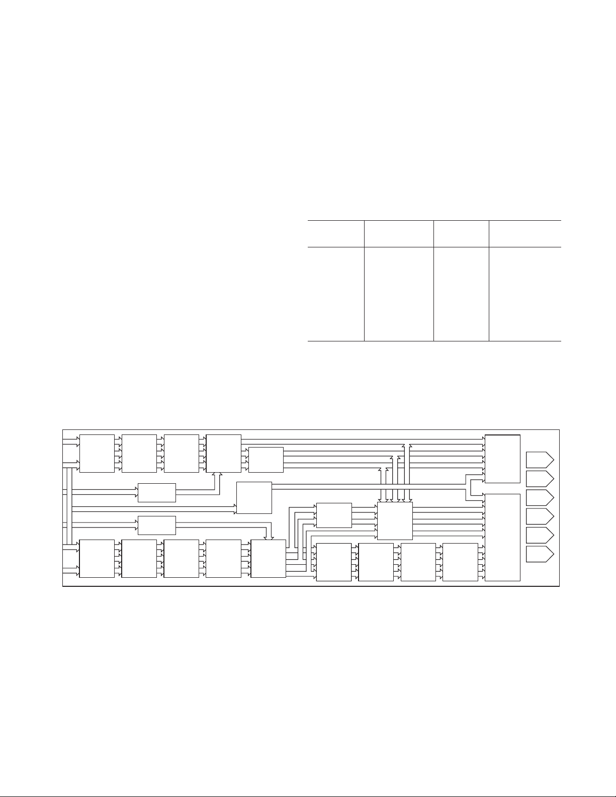
DETAILED FUNCTIONAL BLOCK DIAGRAM
HD PIXEL
INPUT
CLKIN_B
_HSYNC
_VSYNC
_BLANK
S_HSYNC
S_VSYNC
S_BLANK
CLKIN_A
SD PIXEL
INPUT
DEINTER-
LEAVE
DEINTER-
LEAVE
Y
TEST
CR
PATTERN
CB
CB
TEST
CR
PATTERN
Y
TIMING
GENERATOR
TIMING
GENERATOR
SHARPNESS
AND
ADAPTIVE
FILTER
CONT
ROL
DNR
GAMMA
Y COLOR
CR COLOR
CB COLOR
COLOR
CONTROL
CLOCK
CONTROL
AND PLL
INSERTION
4:2:2
TO
4:4:4
SYNC
U
UV SSAF
V
LUMA
CHROMA
FILTERS
AND
2 OVER-
SAMPLING
RGB
MATRIX
F
SC
MODULA-
TION
CGMS
WSS
PS 8
HDTV 2
SD 16
DAC
DAC
DAC
DAC
DAC
DAC
REV. 0–2–

TABLE OF CONTENTS
ADV7314
FEATURES . . . . . . . . . . . . . . . . . . . . . . . . . . . . . . . . . . . . . 1
GENERAL FEATURES . . . . . . . . . . . . . . . . . . . . . . . . . . . . 1
APPLICATIONS . . . . . . . . . . . . . . . . . . . . . . . . . . . . . . . . . 1
SIMPLIFIED FUNCTIONAL BLOCK DIAGRAM . . . . . . 1
GENERAL DESCRIPTION . . . . . . . . . . . . . . . . . . . . . . . . . 1
DETAILED FEATURES . . . . . . . . . . . . . . . . . . . . . . . . . . . 2
DETAILED FUNCTIONAL BLOCK DIAGRAM . . . . . . . 2
SPECIFICATIONS . . . . . . . . . . . . . . . . . . . . . . . . . . . . . . . 4
DYNAMIC SPECIFICATIONS . . . . . . . . . . . . . . . . . . . . . 5
TIMING SPECIFICATIONS . . . . . . . . . . . . . . . . . . . . . . . 6
ABSOLUTE MAXIMUM RATINGS . . . . . . . . . . . . . . . . 14
ORDERING GUIDE . . . . . . . . . . . . . . . . . . . . . . . . . . . . . 14
PIN CONFIGURATION . . . . . . . . . . . . . . . . . . . . . . . . . . 15
PIN FUNCTION DESCRIPTIONS . . . . . . . . . . . . . . . . . 15
TERMINOLOGY . . . . . . . . . . . . . . . . . . . . . . . . . . . . . . . . 16
MPU PORT DESCRIPTION . . . . . . . . . . . . . . . . . . . . . . . 17
REGISTER ACCESS . . . . . . . . . . . . . . . . . . . . . . . . . . . . . 18
Register Programming . . . . . . . . . . . . . . . . . . . . . . . . . . . 18
Subaddress Register (SR7–SR0) . . . . . . . . . . . . . . . . . . . 18
INPUT CONFIGURATION . . . . . . . . . . . . . . . . . . . . . . . 31
Standard Definition Only . . . . . . . . . . . . . . . . . . . . . . . . . 31
Progressive Scan Only or HDTV Only . . . . . . . . . . . . . . . 31
Simultaneous Standard Definition
and Progressive Scan or HDTV . . . . . . . . . . . . . . . . . . 32
Progressive Scan At 27 Mhz (Dual Edge)
or 54 MHz . . . . . . . . . . . . . . . . . . . . . . . . . . . . . . . . . . 32
OUTPUT CONFIGURATION . . . . . . . . . . . . . . . . . . . . . 34
TIMING MODES . . . . . . . . . . . . . . . . . . . . . . . . . . . . . . . 35
HD Async Timing Mode . . . . . . . . . . . . . . . . . . . . . . . . . 35
HD Timing Reset . . . . . . . . . . . . . . . . . . . . . . . . . . . . . . 36
SD Real-Time Control, Subcarrier Reset,
and Timing Reset . . . . . . . . . . . . . . . . . . . . . . . . . . . . . 37
Reset Sequence . . . . . . . . . . . . . . . . . . . . . . . . . . . . . . . . 38
SD VCR FF/RW Sync . . . . . . . . . . . . . . . . . . . . . . . . . . . 38
Vertical Blanking Interval . . . . . . . . . . . . . . . . . . . . . . . . . 39
SD Subcarrier Frequency Registers . . . . . . . . . . . . . . . . . 39
Square Pixel Timing . . . . . . . . . . . . . . . . . . . . . . . . . . . . 39
FILTER SECTION . . . . . . . . . . . . . . . . . . . . . . . . . . . . . . 40
HD Sinc Filter . . . . . . . . . . . . . . . . . . . . . . . . . . . . . . . . . 40
SD Internal Filter Response . . . . . . . . . . . . . . . . . . . . . . . 41
Typical Performance Characteristics . . . . . . . . . . . . . . . . . . 42
COLOR CONTROLS AND RGB MATRIX . . . . . . . . . . . 46
HD/PS Y Level, Cr Level, Cb Level . . . . . . . . . . . . . . . . 46
HD RGB Matrix . . . . . . . . . . . . . . . . . . . . . . . . . . . . . . . 46
Programming the RGB Matrix . . . . . . . . . . . . . . . . . . . . . 46
SD Luma and Color Control . . . . . . . . . . . . . . . . . . . . . . 46
SD Hue Adjust Value . . . . . . . . . . . . . . . . . . . . . . . . . . . . 47
SD Brightness Control . . . . . . . . . . . . . . . . . . . . . . . . . . . 47
SD Brightness Detect . . . . . . . . . . . . . . . . . . . . . . . . . . . . 47
Double Buffering . . . . . . . . . . . . . . . . . . . . . . . . . . . . . . . 47
PROGRAMMABLE DAC GAIN CONTROL . . . . . . . . . . 48
Gamma Correction . . . . . . . . . . . . . . . . . . . . . . . . . . . . . 49
HD Sharpness Filter Control and Adaptive Filter
Control . . . . . . . . . . . . . . . . . . . . . . . . . . . . . . . . . . . . . 50
HD Sharpness Filter and Adaptive Filter Application
Examples . . . . . . . . . . . . . . . . . . . . . . . . . . . . . . . . . . . 51
SD DIGITAL NOISE REDUCTION . . . . . . . . . . . . . . . . 53
Coring Gain Border . . . . . . . . . . . . . . . . . . . . . . . . . . . . . 53
Coring Gain Data . . . . . . . . . . . . . . . . . . . . . . . . . . . . . . 53
DNR Threshold . . . . . . . . . . . . . . . . . . . . . . . . . . . . . . . . 53
Border Area . . . . . . . . . . . . . . . . . . . . . . . . . . . . . . . . . . . 53
Block Size Control . . . . . . . . . . . . . . . . . . . . . . . . . . . . . . 54
DNR Input Select Control . . . . . . . . . . . . . . . . . . . . . . . . 54
DNR Mode Control . . . . . . . . . . . . . . . . . . . . . . . . . . . . . 54
Block Offset Control . . . . . . . . . . . . . . . . . . . . . . . . . . . . 54
SD ACTIVE VIDEO EDGE . . . . . . . . . . . . . . . . . . . . . . . . 55
SAV/EAV Step Edge Control . . . . . . . . . . . . . . . . . . . . . . 55
BOARD DESIGN AND LAYOUT CONSIDERATIONS . 56
DAC Termination and Layout Considerations . . . . . . . . 56
Video Output Buffer and Optional Output Filter . . . . . . . 56
PC BOARD LAYOUT CONSIDERATIONS . . . . . . . . . . 58
Supply Decoupling . . . . . . . . . . . . . . . . . . . . . . . . . . . . . . 58
Digital Signal Interconnect . . . . . . . . . . . . . . . . . . . . . . . 58
Analog Signal Interconnect . . . . . . . . . . . . . . . . . . . . . . . 58
APPENDIX 1—COPY GENERATION MANAGEMENT
SYSTEM . . . . . . . . . . . . . . . . . . . . . . . . . . . . . . . . . . . . . 60
PS CGMS Data Registers 2–0 . . . . . . . . . . . . . . . . . . . . . 60
SD CGMS Data Registers 2–0 . . . . . . . . . . . . . . . . . . . . . 60
Function of CGMS Bits . . . . . . . . . . . . . . . . . . . . . . . . . . 60
CGMS Functionality . . . . . . . . . . . . . . . . . . . . . . . . . . . . 60
APPENDIX 2—SD WIDE SCREEN SIGNALING . . . . . . 62
APPENDIX 3—SD CLOSED CAPTIONING . . . . . . . . . . 63
APPENDIX 4—TEST PATTERNS . . . . . . . . . . . . . . . . . . 64
APPENDIX 5—SD TIMING MODES . . . . . . . . . . . . . . . 66
Mode 0 (CCIR-656)—Slave Option . . . . . . . . . . . . . . . . 66
Mode 0 (CCIR-656)—Master Option . . . . . . . . . . . . . . . 67
Mode 1—Slave Option . . . . . . . . . . . . . . . . . . . . . . . . . . . 68
Mode 1—Master Option . . . . . . . . . . . . . . . . . . . . . . . . . 69
Mode 2—Slave Option . . . . . . . . . . . . . . . . . . . . . . . . . . . 70
Mode 2—Master Option . . . . . . . . . . . . . . . . . . . . . . . . . 71
Mode 3—Master/Slave Option . . . . . . . . . . . . . . . . . . . . . 72
APPENDIX 6—HD TIMING . . . . . . . . . . . . . . . . . . . . . . 73
APPENDIX 7—VIDEO OUTPUT LEVELS . . . . . . . . . . . 74
HD YPrPb Output Levels . . . . . . . . . . . . . . . . . . . . . . . . 74
RGB Output Levels . . . . . . . . . . . . . . . . . . . . . . . . . . . . . 75
YPrPb Output Levels . . . . . . . . . . . . . . . . . . . . . . . . . . . . 76
APPENDIX 8—VIDEO STANDARDS . . . . . . . . . . . . . . . 80
OUTLINE DIMENSIONS . . . . . . . . . . . . . . . . . . . . . . . . . 82
REV. 0
–3–

ADV7314–SPECIFICATIONS
(VAA = 2.375 V–2.625 V, VDD = 2.375 V–2.625 V; V
V
= 1.235 V, R
REF
= 3040 , R
SET
= 150 . All specifications T
LOAD
(0C to 70C), unless otherwise noted.)
= 2.375 V–3.6 V,
DD_IO
MIN
to T
MAX
Parameter Min Typ Max Unit Test Conditions
STATIC PERFORMANCE
1
Resolution 14 Bits
Integral Nonlinearity 2.0 LSB
Differential Nonlinearity
Differential Nonlinearity
2
, +ve 1.0 LSB
2
, –ve 3.0 LSB
DIGITAL OUTPUTS
Output Low Voltage, V
Output High Voltage, V
OL
OH
2.4 [2.0]
3
Three-State Leakage Current ± 1.0 mAV
0.4 [0.4]3VI
VI
= 3.2 mA
SINK
= 400 mA
SOURCE
= 0.4 V, 2.4 V
IN
Three-State Output Capacitance 2 pF
DIGITAL AND CONTROL INPUTS
Input High Voltage, V
Input Low Voltage, V
IH
IL
Input Leakage Current 3 mAV
Input Capacitance, C
IN
2V
0.8 V
= 2.4 V
IN
2pF
ANALOG OUTPUTS
Full-Scale Output Current 4.1 4.33 4.6 mA
Output Current Range 4.1 4.33 4.6 mA
DAC-to-DAC Matching 1.0 %
Output Compliance Range, V
Output Capacitance, C
OC
OUT
0 1.0 1.4 V
7pF
VOLTAGE REFERENCE
Internal Reference Range, V
External Reference Range, V
Current
V
REF
4
REF
REF
1.15 1.235 1.3 V
1.15 1.235 1.3 V
± 10 mA
POWER REQUIREMENTS
Normal Power Mode
5
I
DD
170 mA SD Only [16]
110 mA PS Only [8]
I
DD_IO
I
AA
7, 8
95 mA HDTV Only [2]
172 190
1.0 mA
39 45 mA
6
mA SD [16, 10 Bit] + PS [8, 20 Bit]
Sleep Mode
I
DD
I
AA
I
DD_IO
200 mA
10 mA
250 mA
Power Supply Rejection Ratio 0.01 %/%
NOTES
1
Oversampling disabled. Static DAC performance will be improved with increased oversampling ratios.
2
DNL measures the deviation of the actual DAC output voltage step from the ideal. For +ve DNL, the actual step value lies above the ideal step value; for –ve DNL,
the actual step value lies below the ideal step value.
3
Value in brackets for V
4
External current required to overdrive internal V
5
IDD, the circuit current, is the continuous current required to drive the digital core.
6
Guaranteed maximum by characterization.
7
IAA is the total current required to supply all DACs including the V
8
All DACs on.
Specifications subject to change without notice.
= 2.375 V–2.75 V.
DD_IO
REF
.
circuitry and the PLL circuitry.
REF
REV. 0–4–

ADV7314
(VAA = 2.375 V–2.625 V, VDD = 2.375 V–2.625 V; V
DYNAMIC SPECIFICATIONS
Parameter Min Typ Max Unit Test Conditions
PROGRESSIVE SCAN MODE
Luma Bandwidth 12.5 MHz
Chroma Bandwidth 5.8 MHz
SNR 65.6 dB Luma Ramp Unweighted
SNR 72 dB Flat Field Full Bandwidth
HDTV MODE
Luma Bandwidth 30 MHz
Chroma Bandwidth 13.75 MHz
STANDARD DEFINITION MODE
Hue Accuracy 0.44 ∞
Color Saturation Accuracy 0.20 %
Chroma Nonlinear Gain 0.84 ± %Referenced to 40 IRE
Chroma Nonlinear Phase –0.2 ±∞
Chroma/Luma Intermodulation 0 ±%
Chroma/Luma Gain Inequality 97.5 ± %
Chroma/Luma Delay Inequality 0 ns
Luminance Nonlinearity 0.1 ± %
Chroma AM Noise 84 dB
Chroma PM Noise 75.3 dB
Differential Gain 0.09 % NTSC
Differential Phase 0.12 ∞ NTSC
SNR 63.5 dB Luma Ramp
SNR 77.7 dB Flat Field Full Bandwidth
Specifications subject to change without notice.
3040 , R
= 150 . All specifications T
LOAD
MIN
= 2.375 V–3.6 V, V
DD_IO
to T
(0C to 70C), unless otherwise noted.)
MAX
= 1.235 V, R
REF
SET
=
REV. 0
–5–

ADV7314
TIMING SPECIFICATIONS
(VAA = 2.375 V–2.625 V, VDD = 2.375 V–2.625 V; V
3040 , R
= 150 . All specifications T
LOAD
MIN
= 2.375 V–3.6 V, V
DD_IO
to T
(0C to 70C), unless otherwise noted.)
MAX
= 1.235 V, R
REF
Parameter Min Typ Max Unit Conditions
MPU PORT
1
SCLOCK Frequency 0 400 kHz
SCLOCK High Pulsewidth, t
SCLOCK Low Pulsewidth, t
Hold Time (Start Condition), t
1
2
3
0.6 ms
1.3 ms
0.6 msThe first clock is generated after
this period
Setup Time (Start Condition), t
4
0.6 msRelevant for repeated start
condition
Data Setup Time, t
SDATA, SCLOCK Rise Time, t
SDATA, SCLOCK Fall Time, t
Setup Time (Stop Condition), t
5
6
7
8
100 ns
300 ns
300 ns
0.6 ms
RESET Low Time 100 ns
ANALOG OUTPUTS
Analog Output Delay
2
7ns
Output Skew 1 ns
CLOCK CONTROL AND PIXEL PORT
f
CLK
f
CLK
Clock High Time t
Clock Low Time t
Data Setup Time t
Data Hold Time t
SD Output Access Time t
SD Output Hold Time t
HD Output Access Time t
HD Output Hold Time t
PIPELINE DELAY
9
10
1
11
1
12
13
14
13
14
4
3
27 MHz Progressive Scan Mode
81 MHz HDTV Mode/ASYNC Mode
40 % of one clk cycle
40 % of one clk cycle
2.0 ns
2.0 ns
15 ns
5.0 ns
14 ns
5.0 ns
63 clk cycles SD [2, 16]
76 clk cycles SD Component Mode [16]
35 clk cycles PS [1]
41 clk cycles PS [8]
36 clk cycles HD [2, 1]
NOTES
1
Guaranteed by characterization.
2
Output delay measured from the 50% point of the rising edge of CLOCK to the 50% point of DAC output full-scale transition.
3
Data: C [9:0]; Y [9:0], S[9:0]
Control: P_HSYNC, P_VSYNC, P_BLANK, S_HSYNC, S_VSYNC, S_BLANK.
4
SD, PS = 27 MHz, HD = 74.25 MHz.
Specifications subject to change without notice.
SET
=
REV. 0–6–
CLKIN_A
ADV7314
t
12
t
13
t
14
CONTROL
INPUTS
t
= CLOCK HIGH TIME
9
t
= CLOCK LOW TIME
10
t
= DATA SETUP TIME
11
t
= DATA HOLD TIME
12
P_HSYNC,
P_VSYN
P_BLANK
Y9–Y0
C9–C0
CONTROL
OUTPUTS
t
t
9
10
C,
Y0 Y1 Y2 Y3 Y4 Y5
Cb0 Cr0 Cb2 Cr2 Cb4 Cr4
t11
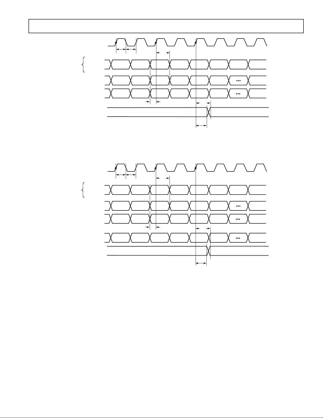
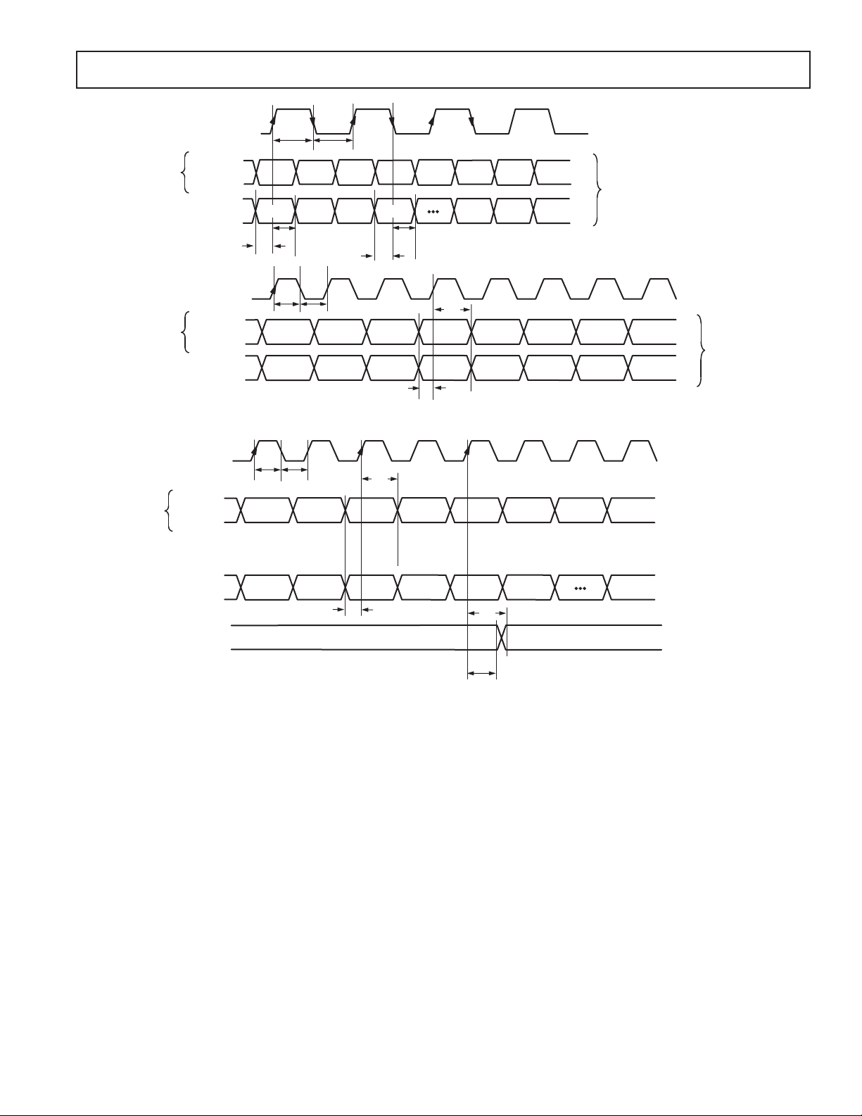
Figure 1. HD Only 4:2:2 Input Mode [Input Mode 010]; PS Only 4:2:2 Input Mode [Input Mode 001]
CLKIN_A
t
12
CONTROL
INPUTS
P_HSYNC,
P_VSYNC,
P_BLANK
Y9–Y0
t
t
9
10
Y0 Y1 Y2 Y3 Y4 Y5
Cb0 Cb1 Cb2 Cb3 Cb4 Cb5
t
11
Cr0 Cr1 Cr2 Cr3 Cr5
Cr4
t
13
t
14
CONTROL
OUTPUTS
t
= CLOCK HIGH TIME
9
t
= CLOCK LOW TIME
10
t
= DATA SETUP TIME
11
t
= DATA HOLD TIME
12
C9–C0
S9–S0
Figure 2. HD Only 4:4:4 Input Mode [Input Mode 010]; PS Only 4:4:4 Input Mode [Input Mode 001]
REV. 0
–7–

ADV7314
CONTROL
INPUTS
CLKIN_A
P_HSYNC,
P_VSYNC,
P_BLANK
t
t
9
10
t
12
CONTROL
OUTPUTS
t
= CLOCK HIGH TIME
9
t
= CLOCK LOW TIME
10
t
= DATA SETUP TIME
11
t
= DATA HOLD TIME
12
Y9–Y0
C9–C0
S9–S0
G0 G1 G2 G3 G4 G5
B0 B1 B2 B3 B4 B5
t
11
R0 R1 R2 R3 R4 R5
Figure 3. HD RGB 4:4:4 Input Mode [Input Mode 010]
CLKIN_B*
t9
t10
CONTROL
INPUTS
t
= CLOCK HIGH TIME
9
t
= CLOCK LOW TIME
10
t
= DATA SETUP TIME
11
t
= DATA HOLD TIME
12
P_HSYNC,
P_VSYNC,
P_BLANK
Y9–Y
CONTROL
OUTPUTS
Cb0 Y0 Cr0 Y1 Crxxx Yxxx
0
t12
t11
*CLKIN_B MUST BE USED IN THIS PS MODE.
Figure 4. PS 4:2:2 110-Bit Interleaved at 27 MHz
t
13
t
14
t12
t11
t13
t14
HSYNC/VSYNC
Input Mode [Input Mode 100]
REV. 0–8–

CONTROL
INPUTS
CLKIN_A
P_HSYNC,
P_VSYNC,
P_BLANK
t9
ADV7314
t10
Y9–Y0
CONTROL
OUTPUTS
t
= CLOCK HIGH TIME
9
t
= CLOCK LOW TIME
10
t
= DATA SETUP TIME
11
t
= DATA HOLD TIME
12
Figure 5. PS 4:2:2 110-Bit Interleaved at 54 MHz
t
= CLOCK HIGH TIME
9
t
= CLOCK LOW TIME
10
t
= DATA SETUP TIME
11
t
= DATA HOLD TIME
12
Cb0 Y0 Cr0 Y1 Crxxx Yxxx
t11
CLKIN_B*
Y9–Y
CONTROL
OUTPUTS
t12
t
t
9
3FF 00 00 XY Cb0 Y0 Cr0 Y1
0
t
12
t
11
*CLKIN_B USED IN THIS PS ONLY MODE.
10
t13
t14
HSYNC/VSYNC
t
12
t
11
t
13
t
14
Input Mode [Input Mode 111]
Figure 6. PS Only 4:2:2 110-Bit Interleaved at 27 MHz EAV/SAV Input Mode [Input Mode 100]
REV. 0
CLKIN_A
t10
t9
CONTROL
OUTPUTS
t
= CLOCK HIGH TIME
9
t
= CLOCK LOW TIME
10
t
= DATA SETUP TIME
11
t
= DATA HOLD TIME
12
Y9–Y0
3FF 00 00 XY Cb0 Y0 Cr0 Y1
t11
t12
NOTE: Y0, Cb0 SEQUENCE AS PER SUBADDRESS 0x01 BIT 1
t13
t14
Figure 7. PS Only 4:2:2 110-Bit Interleaved at 54 MHz EAV/SAV Input Mode [Input Mode 111]
–9–
ADV7314
CONTROL
INPUTS
CLKIN_B
P_HSYNC,
P_VSYNC,
P_BLANK
t
t
t
10
9
12
CONTROL
INPUTS
Y9–Y0
C9–C0
CLKIN_A
S_HSYNC,
S_VSYNC,
S_BLANK
S9–S0
Y0 Y1
Cb0 Cr0 Cb2
t
t
9
10
Cb0 Y0 Cr0
Y2
t
11
Y3 Y4 Y5
Cr2
Y1
t
11
t
12
Cb4 Cr4
Cb1 Y2
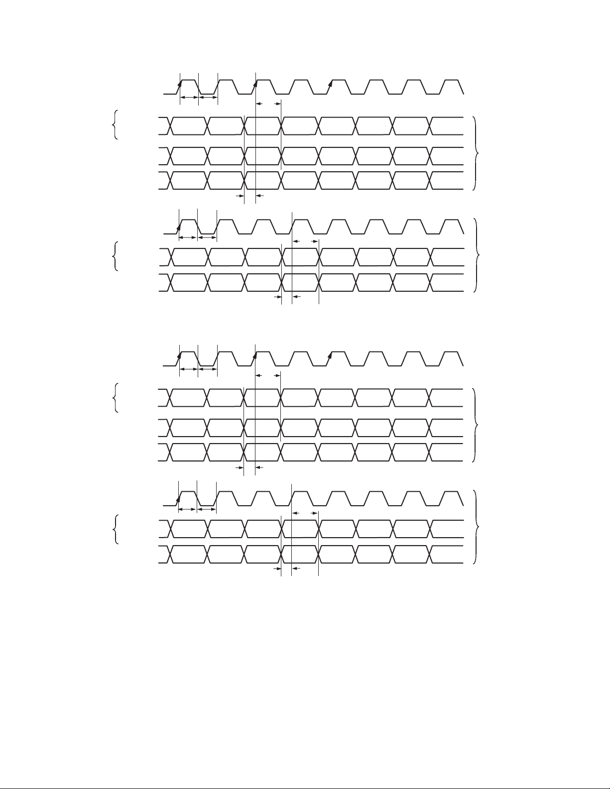
Figure 8. HD 4:2:2 and SD (10-Bit) Simultaneous Input Mode [Input Mode 101]; SD Oversampled
[Input Mode 110] HD Oversampled
CLKIN_B
t12
Y2
Y3 Y4 Y5
CONTROL
INPUTS
P_HSYNC,
P_VSYNC,
P_BLANK
Y9–Y0
t10
t9
Y0 Y1
HD INPUT
SD INPUT
PS INPUT
CONTROL
INPUTS
C9–C0
CLKIN_A
S_HSYNC,
S_VSYNC,
S_BLANK
S9–S0
Cb0 Cr0 Cb2
t11
t9
t10
Cb0 Y0 Cr0
t11
Cr2
Y1
Cb4 Cr4
t12
Cb1 Y2
Figure 9. PS (4:2:2) and SD (10-Bit) Simultaneous Input Mode [Input Mode 011]
SD INPUT
REV. 0–10–
CONTROL
INPUTS
CONTROL
INPUTS
CONTROL
INPUTS
CLKIN_B
t
10
PS INPUT
Crxxx Yxxx
t
12
t
11
t
t
10
12
Y1
t
11
Cb1 Y2
P_HSYNC,
P_VSYNC,
P_BLANK
Y9–Y0
CLKIN_A
S_HSYNC,
S_VSYNC,
S_BLANK
S9–S0
t
9
Cb0 Y0 Cr0 Y1
t
12
t
11
t
9
Cb0 Y0 Cr0
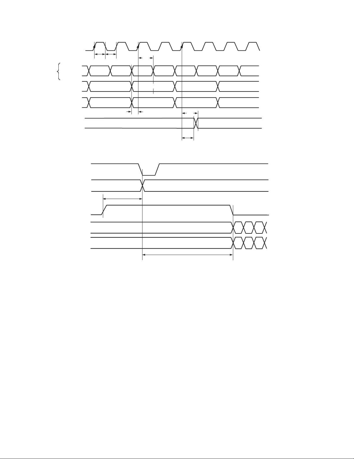
Figure 10. PS (10-Bit) and SD (10-Bit) Simultaneous Input Mode [Input Mode 100]
CLKIN_A
t
12
S_HSYNC,
S_VSYNC,
S_BLANK
t
t
9
10
ADV7314
SD INPUT
IN SLAVE MODE
S9–S0/Y9–Y0*
CONTROL
OUTPUTS
*SELECTED BY ADDRESS 0x01 BIT 7
Figure 11. 10-/8-Bit SD Only Pixel Input Mode [Input Mode 000]
Cb0 Cr0 Cb2 Cr2 Cb4 Cr4
t
11
t
13
t
14
IN MASTER/SLAVE MODE
REV. 0
–11–
ADV7314
P
CONTROL
INPUTS
CLKIN_A
S_HSYNC,
S_VSYNC,
S_BLANK
t
t
9
10
t
12
IN SLAVE MODE
S9–S0/Y9–Y0*
C9–C0
CONTROL
OUTPUTS
*SELECTED BY ADDRESS 0x01 BIT 7
Figure 12. 20-/16-Bit SD Only Pixel Input Mode [Input Mode 000]
_HSYNC
P_VSYNC
P_BLANK
Y9–Y0
C9–C0
Y0 Y2 Y3
Cb0 Cr0 Cb2 Cr2
t
11
A
Y1
t
13
t
14
Y0 Y1
Cb0 Cr0
IN MASTER/SLAVE MODE
Y2 Y3
Cr1 Cb1
B
A = 16 CLK CYCLES FOR 525p
A = 12 CLK CYCLES FOR 626p
A = 44 CLK CYCLES FOR 1080i @ 30Hz, 25Hz
A = 70 CLK CYCLES FOR 720p
AS RECOMMENDED BY STANDARD
B (MIN) = 122 CLK CYCLES FOR 525p
B (MIN) = 132 CLK CYCLES FOR 625p
B (MIN) = 236 CLK CYCLES FOR 1080i @ 30Hz, 25Hz
B (MIN) = 300 CLK CYCLES FOR 720p
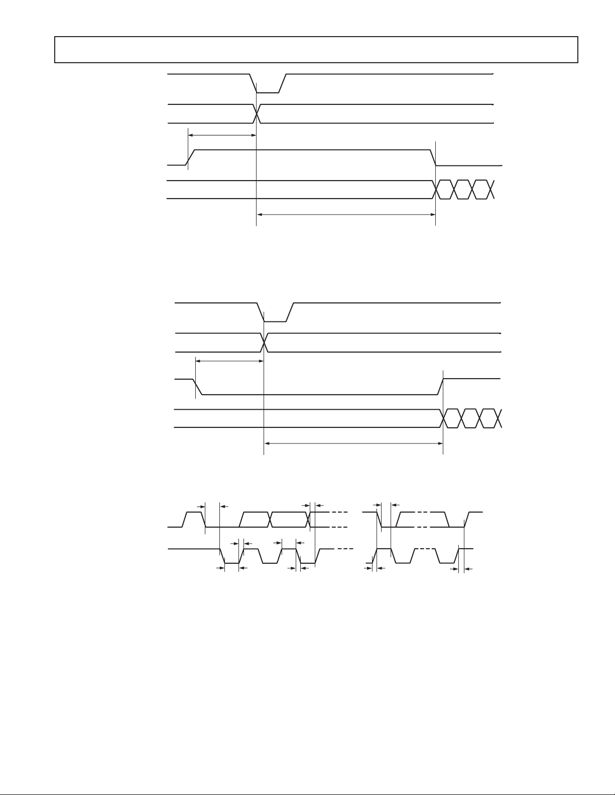
Figure 13. HD 4:2:2 Input Timing Diagram
REV. 0–12–
P
_HSYNC
P_VSYNC
P_BLANK
ADV7314
a
Y9–Y0
a = 32 CLK CYCLES FOR 525p
a = 24 CLK CYCLES FOR 625p
AS RECOMMENDED BY STANDARD
b(MIN) = 244 CLK CYCLES FOR 525p
b(MIN) = 264 CLK CYCLES FOR 625p
Figure 14. PS 4:2:2 110-Bit Interleaved Input Timing Diagram
S_HSYNC
S_VSYNC
PAL = 24 CLKCYCLES
NTSC = 32 CLKCYCLES
S_BLANK
S9–S0/Y9–Y0*
*SELECTED BY ADDRESS 0x01 BIT 7
Figure 15. SD Timing Input for Timing Mode 1
Cb Y
Cr Y
Cr Y
Cb Y
b
PAL = 24 CLK CYCLES
NTSC = 32 CLK CYCLES
t
3
t
4
t
8
SDA
SCLK
t
3
t
6
t
2
t
5
t
1
t
7
Figure 16. MPU Port Timing Diagram
REV. 0
–13–

ADV7314
ABSOLUTE MAXIMUM RATINGS*
VAA to AGND . . . . . . . . . . . . . . . . . . . . . . . . +3.0 V to –0.3 V
to GND . . . . . . . . . . . . . . . . . . . . . . . . . +3.0 V to –0.3 V
V
DD
V
to IO_GND . . . . . . . . . . . . –0.3 V to V
DD_IO
Ambient Operating Temperature (T
Storage Temperature (T
) . . . . . . . . . . . . . . .–65∞C to +150∞C
S
A
) . . . . . . . . . 0∞C to 70∞C
DD_IO
to +0.3 V
Infrared Reflow Soldering (20 secs) . . . . . . . . . . . . . . . . 260∞C
*Stresses above those listed under Absolute Maximum Ratings may cause perma-
nent damage to the device. This is a stress rating only; functional operation of the
device at these or any other conditions above those listed in the operational sections
of this specification is not implied. Exposure to absolute maximum rating conditions for extended periods may affect device reliability.
The ADV7314 is a Pb-free environmentally friendly product. It is
manufactured using the most up-to-date materials and processes.
The coating on the leads of each device is 100% pure Sn electroplate. The device is suitable for Pb-free applications and is able to
withstand surface-mount soldering at up to 255∞C [± 5∞C]. In
addition, it is backward compatible with conventional SnPb soldering processes. This means that the electroplated Sn coating can
be soldered with Sn/Pb solder pastes at conventional reflow temperatures of 220∞C to 235∞C.
ORDERING GUIDE*
Model Package Description Package Option
THERMAL CHARACTERISTICS
JC = 11∞C/W
= 47∞C/W
JA
ADV7314KST Plastic Quad Flatpack ST-64
(LQFP)
*Analog output short circuit to any power supply or common can be of an indefi-
nite duration.
CAUTION
ESD (electrostatic discharge) sensitive device. Electrostatic charges as high as 4000 V readily
accumulate on the human body and test equipment and can discharge without detection. Although the
ADV7314 features proprietary ESD protection circuitry, permanent damage may occur on devices
subjected to high energy electrostatic discharges. Therefore, proper ESD precautions are recommended
to avoid performance degradation or loss of functionality.
REV. 0–14–
PIN CONFIGURATION
K
DD
GND_IO
CLKN_BS9S8S7S6S5DGND
V
S4S3S2S1S0
S_HSYNCS_VSYNC
49505152535455565758596061626364
ADV7314
V
DD_IO
V
DGND
1
PIN 1
2
Y0
Y1
Y2
Y3
Y4
Y5
Y6
Y7
DD
Y8
Y9
C0
C1
C2
10
11
12
13
14
15
16
3
4
5
6
7
8
9
IDENTIFIER
2
C3
C4
C
I
ALSB
SDA
ADV7314
LQFP
TOP VIEW
(Not to Scale)
SCLK
P_VSYNC
P_BLANK
P_HSYNC
C5C6C7C8C9
48
47
46
45
44
43
42
41
40
39
38
37
36
35
34
33
32313029282726252423222120191817
CLKIN_A
RTC_SCR_TR
S_BLAN
R
SET1
V
REF
COMP1
DAC A
DAC B
DAC C
V
AA
AGND
DAC D
DAC E
DAC F
COMP2
R
SET2
EXT_LF
RESET
PIN FUNCTION DESCRIPTIONS
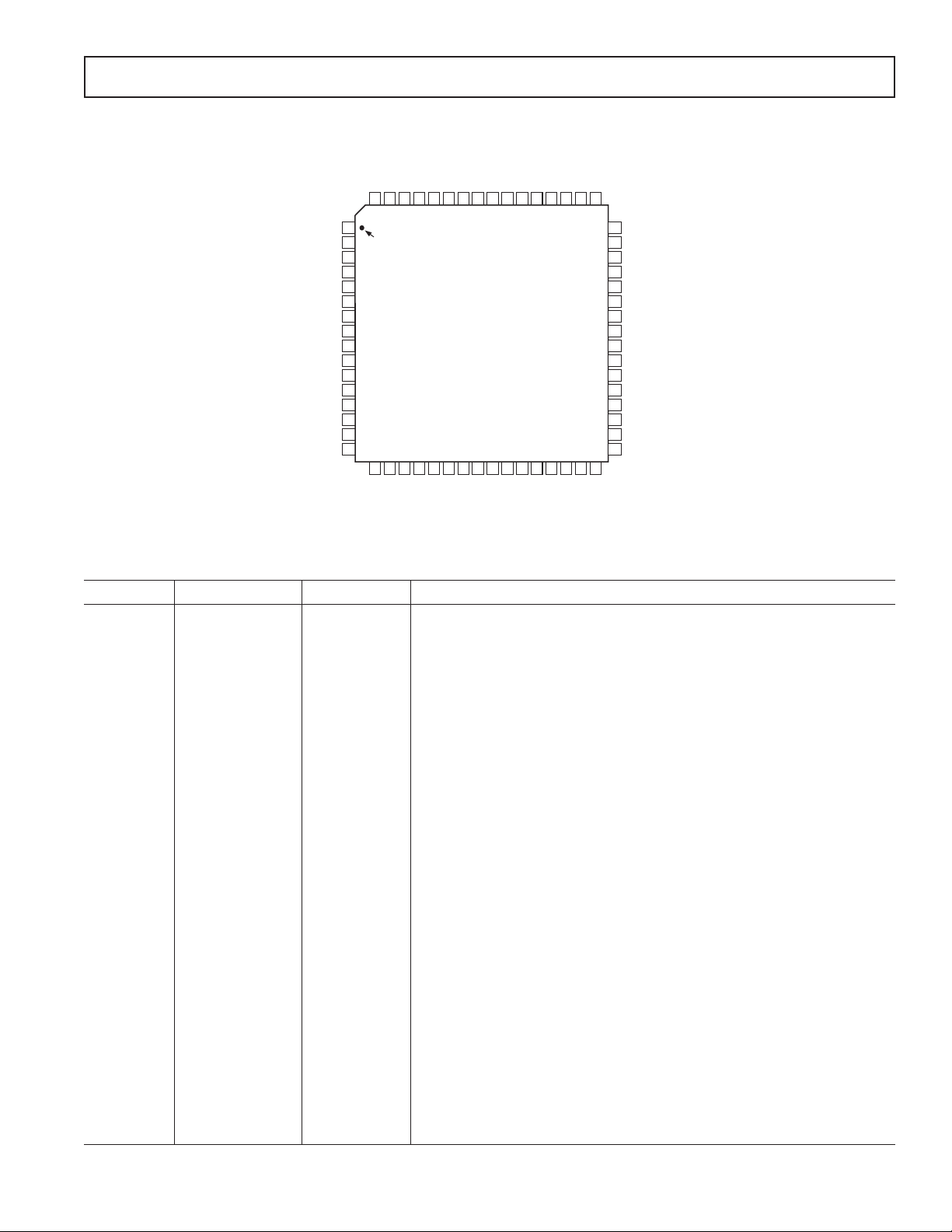
Pin No. Mnemonic Input/Output Function
11, 57 DGND G Digital Ground.
40 AGND G Analog Ground.
32 CLKIN_A I Pixel Clock Input for HD (74.25 MHz Only, PS Only (27 MHz), SD Only
(27 MHz).
63 CLKIN_B I Pixel Clock Input. Requires a 27 MHz reference clock for Progressive Scan
mode or a 74.25 MHz (74.1758 MHz) reference clock in HDTV mode. This
clock is only used in dual modes.
36, 45 COMP2, COMP1 O Compensation Pin for DACs. Connect 0.1 mF capacitor from COMP pin
to V
.
AA
44 DAC A O CVBS/Green/Y/Y Analog Output.
43 DAC B O Chroma/Blue/U/Pb Analog Output.
42 DAC C O Luma/Red/V/Pr Analog Output.
39 DAC D O In SD Only Mode: CVBS/Green/Y Analog Output.
In HD Only mode and simultaneous HD/SD mode: Y/Green [HD] Analog
Output.
38 DAC E O In SD Only Mode: Luma/Blue/U Analog Output.
In HD Only mode and simultaneous HD/SD mode: Pr/Red Analog Output.
37 DAC F O In SD Only Mode: Chroma/Red/V Analog Output.
In HD Only mode and simultaneous HD/SD mode: Pb/Blue [HD] Analog
Output.
23 P_HSYNC IVideo Horizontal Sync Control Signal for HD in Simultaneous SD/HD Mode
and HD.
24 P_VSYNC IVideo Vertical Sync Control Signal for HD in Simultaneous SD/HD Mode
and HD.
25 P_BLANK I Video Blanking Control Signal for HD in Simultaneous SD/HD Mode and HD.
48 S_BLANK I/O Video Blanking Control Signal for SD only.
REV. 0
–15–

ADV7314
Pin No. Mnemonic Input/Output Function
50 S_HSYNC I/O Video Horizontal Sync Control Signal for SD Only.
49 S_VSYNC I/O Video Vertical Sync Control Signal for SD Only.
2–9, 12–13 Y9–Y0 I SD or Progressive Scan/HDTV Input Port for Y Data. Input port for inter-
leaved progressive scan data. The LSB is set up on Pin Y0. For 8-bit data
input, LSB is set up on Y2.
14–18, 26–30 C9–C0 I Progressive Scan/HDTV Input Port. In 4:4:4 Input mode, this port is used for
the Cb[Blue/U] data. The LSB is set up on Pin C0. For 8-bit data input, LSB
is set up on C2.
51–55, 58–62 S9–S0 I SD or Progressive Scan/HDTV Input Port for Cr [Red/V] Data in 4:4:4 Input
Mode. LSB is set up on Pin S0. For 8-bit data input, LSB is set up on S2.
33 RESET IThis input resets the on-chip timing generator and sets the ADV7314 into
default register setting. RESET is an active low signal.
35, 47 R
22 SCLK I I
21 SDA I/O I
20 ALSB I TTL Address Input. This signal sets up the LSB of the I
1V
10, 56 V
41 V
46 V
34 EXT_LF I External Loop Filter for the Internal PLL.
SET2
DD_IO
DD
AA
REF
, R
SET1
IA 3040 W resistor must be connected from this pin to AGND and is used
to control the amplitudes of the DAC outputs.
2
C Port Serial Interface Clock Input.
2
C Port Serial Data Input/Output.
2
C address. When
this pin is tied low, the I
2
C filter is activated, reducing noise on the I2C
interface.
PPower Supply for Digital Inputs and Outputs.
PDigital Power Supply.
PAnalog Power Supply.
I/O Optional External Voltage Reference Input for DACs or Voltage Reference
Output (1.235 V).
31 RTC_SCR_TR I Multifunctional Input. Real-time control (RTC) input, timing reset input,
subcarrier reset input.
19 I
CIThis input pin must be tied high (V
over the I
2
C port.
) for the ADV7314 to interface
DD_IO
2
64 GND_IO Digital Input/Output Ground.
TERMINOLOGY
SD Standard definition video, conforming to ITU-R BT.601/656.
HD High definition video, such as progressive scan or HDTV.
PS Progressive scan video, conforming to SMPTE 293M, ITU-R BT.1358, BTA T-1004 EDTV2, BTA 1362
HDTV High definition television video, conforming to SMPTE 274M or SMPTE 296M.
YCrCb SD, HD, or PS component digital video.
YPrPb HD, SD, or PS component analog video.
REV. 0–16–
ADV7314
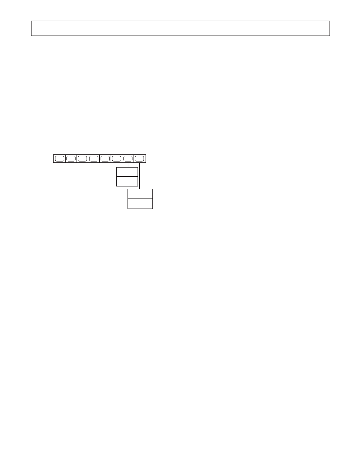
MPU PORT DESCRIPTION
The ADV7314 supports a 2-wire serial (I2C compatible) microprocessor bus driving multiple peripherals. Two inputs, serial
data (SDA) and serial clock (SCL), carry information between
any device connected to the bus. Each slave device is recognized
by a unique address. The ADV7314 has four possible slave
addresses for both read and write operations. These are unique
addresses for each device and are illustrated in Figure 17. The
LSB sets either a read or write operation. Logic 1 corresponds
to a read operation, while Logic 0 corresponds to a write operation. A1 is set by setting the ALSB pin of the ADV7314 to
Logic 0 or Logic 1. When ALSB is set to 1, there is greater
input bandwidth on the I
transfers on this bus. When ALSB is set to 0, there is reduced
input bandwidth on the I
less than 50 ns will not pass into the I
2
C lines, which allows high speed data
2
C lines, which means that pulses of
2
C internal controller.
This mode is recommended for noisy systems.
1 1 0 1 0 1 A1 X
ADDRESS
CONTROL
SET UP BY
ALSB
READ/WRITE
CONTROL
0 WRITE
1 READ
Figure 17. ADV7314 Slave Address = D4h
To control the various devices on the bus, the following protocol
must be followed. First, the master initiates a data transfer by
establishing a start condition, defined by a high-to-low transition
on SDA, while SCL remains high. This indicates that an address/
data stream will follow. All peripherals respond to the start
condition and shift the next eight bits (7-bit address + R/W bit).
The bits are transferred from MSB down to LSB. The peripheral that recognizes the transmitted address responds by pulling
the data line low during the ninth clock pulse. This is known as
an acknowledge bit. All other devices withdraw from the bus at
this point and maintain an idle condition. The idle condition is
when the device monitors the SDA and SCL lines waiting for
the start condition and the correct transmitted address. The
R/W bit determines the direction of the data.
A Logic 0 on the LSB of the first byte means that the master
will write information to the peripheral. A Logic 1 on the LSB
of the first byte means that the master will read information
from the peripheral.
The ADV7314 acts as a standard slave device on the bus. The
data on the SDA pin is eight bits wide, supporting the 7-bit
addresses plus the R/W bit. It interprets the first byte as the
device address and the second byte as the starting subaddress.
There is a subaddress auto-increment facility, which allows data
to be written to or read from registers in ascending subaddress
sequence starting at any valid subaddress. A data transfer is
always terminated by a stop condition. The user can also access
any unique subaddress register on a one-by-one basis without
having to update all the registers.
Stop and start conditions can be detected at any stage during
the data transfer. If these conditions are asserted out of sequence
with normal read and write operations, then these cause an
immediate jump to the idle condition. During a given SCL high
period, the user should issue only one start condition, one stop
condition, or a single stop condition followed by a single start
condition. If an invalid subaddress is issued by the user, the
ADV7314 will not issue an acknowledge and will return to the
idle condition. If in auto-increment mode the user exceeds the
highest subaddress, the following action will be taken:
1. In read mode, the highest subaddress register contents
will continue to be output until the master device issues a
no-acknowledge. This indicates the end of a read. A
no-acknowledge condition is when the SDA line is not
pulled low on the ninth pulse.
2. In write mode, the data for the invalid byte will not be loaded
into any subaddress register, a no-acknowledge will be issued
by the ADV7314, and the part will return to the idle condition.
REV. 0
–17–
ADV7314
Before writing to the subcarrier frequency registers, the ADV7314
must have been reset at least once since power-up.
The four subcarrier frequency registers must be updated starting with subcarrier frequency register 0 through subcarrier
frequency register 3. The subcarrier frequency will not update
until the last subcarrier frequency register byte has been received
by the ADV7314.
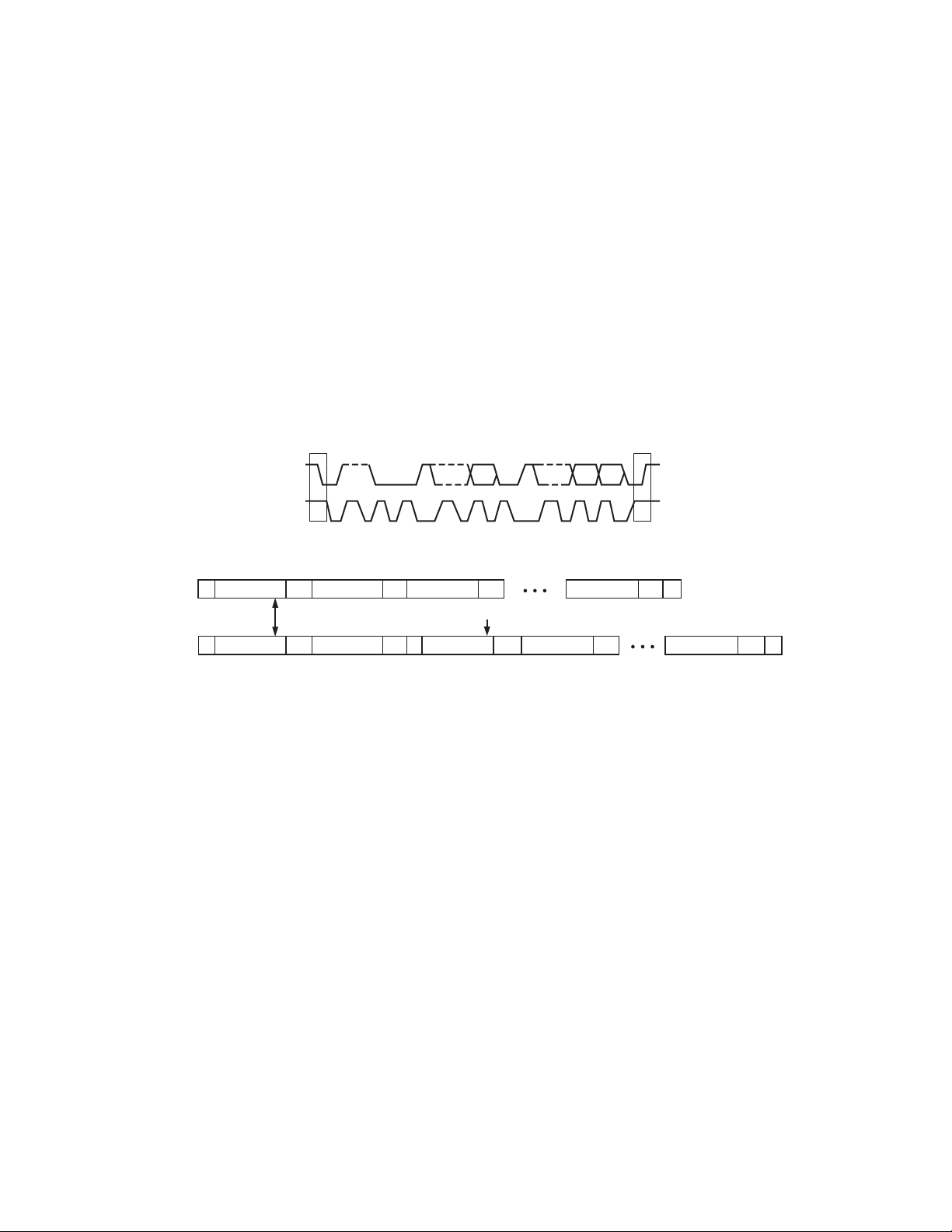
Figure 18 illustrates an example of the data transfer for a write
sequence and the start and stop conditions.
Figure 19 shows bus write and read sequences.
REGISTER ACCESS
The MPU can write to or read from all of the registers of the
ADV7314 except the subaddress registers, which are write-only
registers. The subaddress register determines which register the
SDATA
SCLOCK
S
1–7 8
START ADRR R/W ACK SUBADDRESS ACK DATA ACK STOP
9
1–7 8 9
Figure 18. Bus Data Transfer
next read or write operation accesses. All communications with
the part through the bus start with an access to the subaddress
register. A read/write operation is then performed from/to the
target address, which increments to the next address until a stop
command on the bus is performed.
Register Programming
The following section describes the functionality of each register.
All registers can be read from as well as written to unless otherwise stated.
Subaddress Register (SR7–SR0)
The communications register is an 8-bit write-only register. After
the part has been accessed over the bus and a read/write operation is selected, the subaddress is set up. The subaddress register
determines to/from which register the operation takes place.
1–7
89
P
WRITE
SEQUENCE
READ
SEQUENCE
S SLAVE ADDR A(S) SUB ADDR A(S) DATA A(S) DATA A(S) P
LSB = 0
S SLAVE ADDR A(S) SUB ADDR A(S) S SLAVE ADDR A(S) DATA DATAA(M) A(M) P
S = START BIT
P = STOP BIT
A(S) = ACKNOWLEDGE BY SLAVE
A(M) = ACKNOWLEDGE BY MASTER
LSB = 1
A(S) = NO-ACKNOWLEDGE BY SLAVE
A(M) = NO-ACKNOWLEDGE BY MASTER
Figure 19. Write and Read Sequence
REV. 0–18–
ADV7314
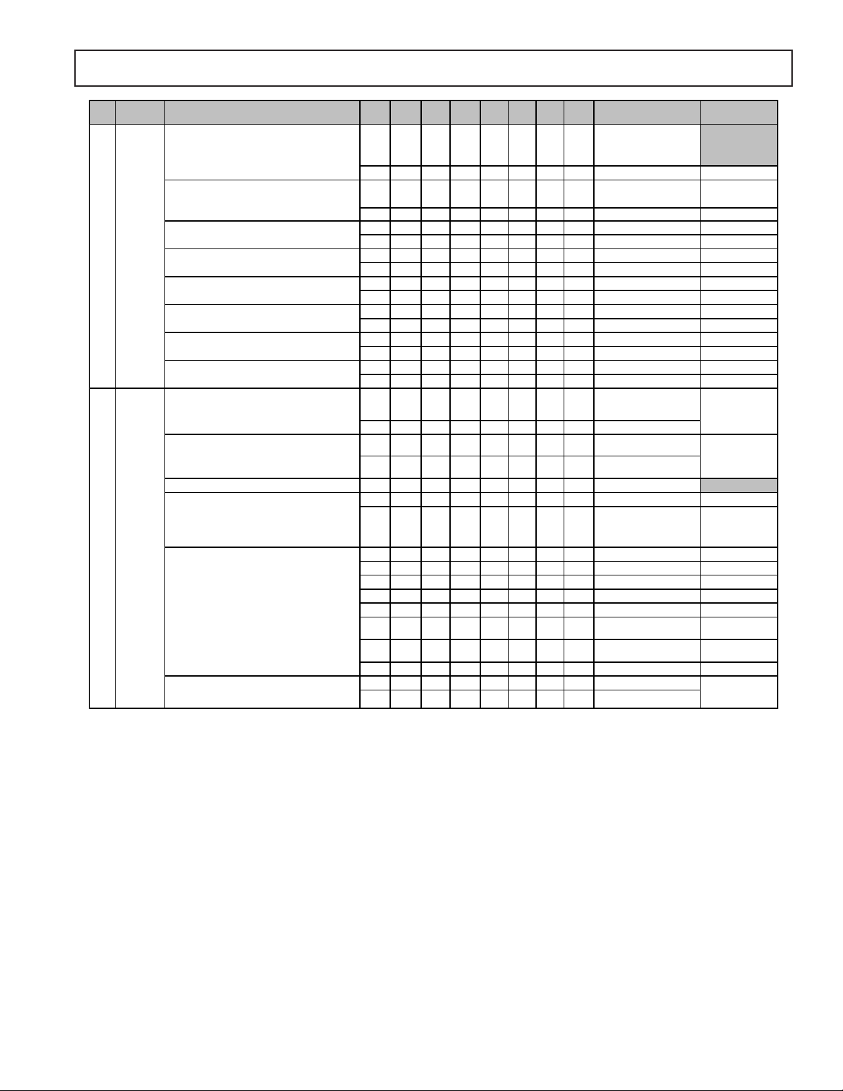
SR7SR0 Register Bit Description Bit 7 Bit 6 Bit 5 Bit 4 Bit 3 Bit 2 Bit 1 Bit 0 Register Setting
00h Power
Mode
Register
Mode Select
01h
Register
Sleep Mode. With this control enabled, the current
consumption is reduced to
the internal PLL cct are disabled. I
be read from and written to in sleep mode.
PLL and Oversampling Control. This control
allows the internal PLL cct to be powered down
and the oversampling to be switched off.
DAC F. Power on/off.
DAC E. Power on/off.
DAC D. Power on/off.
DAC C. Power on/off.
DAC B. Power on/off.
DAC A. Power on/off.
BTA T-1004 or 1362 Compatibility
Clock Edge
Reserved 0 38h
Clock Align
Input Mode
Y/S Bus Swap
A level. All DACs and
2
C registers can
0 DAC F off
1 DAC F on
0 DAC E off
1 DAC E on
0 DAC D off
1 DAC D on
0 DAC D off
1 DAC C on
0 DAC B off
1 DAC B on
0 DAC A off
1 DAC A on
0
1 Must be set if the phase
000 SD input only
001 PS input only
010 HDTV input only
011 SD and PS [20-bit]
100 SD and PS [10-bit]
101 SD and HDTV [SD
110 SD and HDTV [HDTV
111 PS only [at 54 MHz]
0 10-bit data on S Bus
1 10-bit data on Y Bus
0Sleep Mode off FCh
1Sleep Mode on
0 PLL on
1 PLL off
0Disabled
1 Enabled
0 Cb clocked on rising edge
1Y clocked on rising edge
delay between the two
input clocks is <9.25 ns or
>27.75 ns.
oversampled
oversampled]
Register Reset
Value (Shaded)
Only for PS dual
edge clk mode
Only for PS
interleaved input at
27 MHz
Only if two input
clocks are used
SD Only. 10-Bit/
20-Bit Input mode
REV. 0
–19–
ADV7314
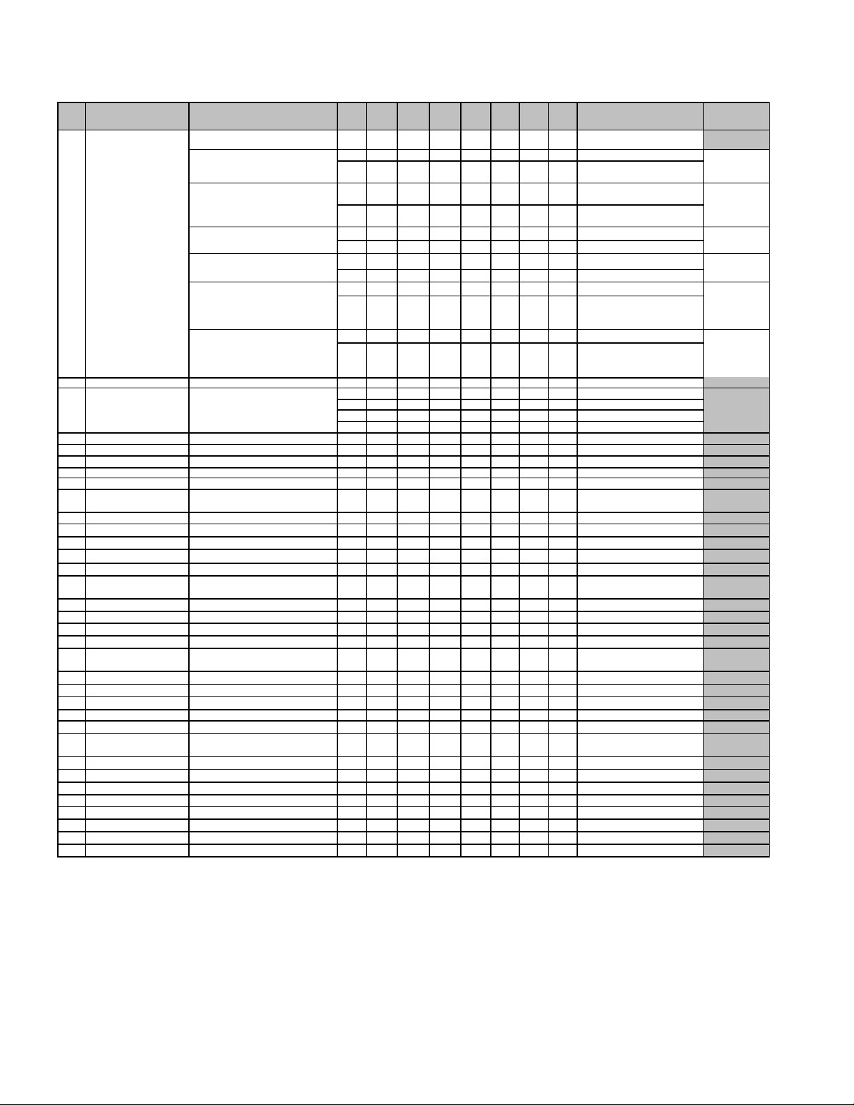
SR7SR0 Register Bit Description Bit 7 Bit 6 Bit 5 Bit 4 Bit 3 Bit 2 Bit 1 Bit 0 Register Setting
02h Mode Register 0 Reserved 00 Zero must be written to
Test Pattern Black Bar 0 Disabled
RGB Matrix 0 Disable Programmable
Sync on RGB
RGB/YUV Output 0 RGB component outputs
SD Sync 0 No Sync output
HD Sync 0 No Sync output
03h RGB Matrix 0 xx LSB for GY 03h
04h RGB Matrix 1 x x LSB for RV F0h
05h RGB Matrix 2 x xxxxxxxBit 9–2 for GY 4Eh
06h RGB Matrix 3 x xxxxxxxBit 9–2 for GU 0Eh
07h RGB Matrix 4 x xxxxxxxBit 9–2 for GV 24h
08h RGB Matrix 5 x xxxxxxxBit 9–2 for BU 92h
09h RGB Matrix 6 x xxxxxxxBit 9–2 for RV 7Ch
0Ah DAC A,B,C Output
0Bh DAC D,E,F Output
0Ch 0 0110011Note 3 00h
0Dh 1 1000000Note 3 00h
0Eh Reserved 00h
0Fh Reserved 00h
1
For more detail, refer to Appendix 7.
2
For more detail on the programmable output levels, refer to the Programmable DAC Gain Control section.
3
Must be written to after power-up/reset.
Level
Level
2
Positive Gain to DAC Output
Voltage
Negative Gain to DAC Output
Voltage
Positive Gain to DAC Output
Voltage
Negative Gain to DAC Output
Voltage
1
1 Output SD syncs on
1 Output HD syncs on
xx LSB for GU
0 00000000% 00h
0 0000001+0.018%
0 00000100.036%
0 0111111+7.382%
0 1000000+7.5%
1 1000000–7.5%
1 1000001–7.382%
1 0000010–7.364%
1 1111111–0.018%
0 00000000% 00h
0 0000001+0.018%
0 00000100.036%
0 0111111+7.382%
0 1000000+7.5%
1 1000000–7.5%
1 1000001–7.382%
1 0000010–7.364%
1 1111111–0.018%
0 No Sync
1 Sync on all RGB outputs
1 YUV component outputs
xx LSB for GV
1 Enabled
1 Enable Programmable
xx LSB for BU
these bits
RGB Matrix
RGB Matrix
S_HSYNC output, S_VSYNC
output, S_BLANK output
P_HSYNC output, P_VSYNC
output, P_BLANK output
………
……….
………
……….
Reset Value
20h
11h, Bit 2 must
be enabled also
REV. 0–20–
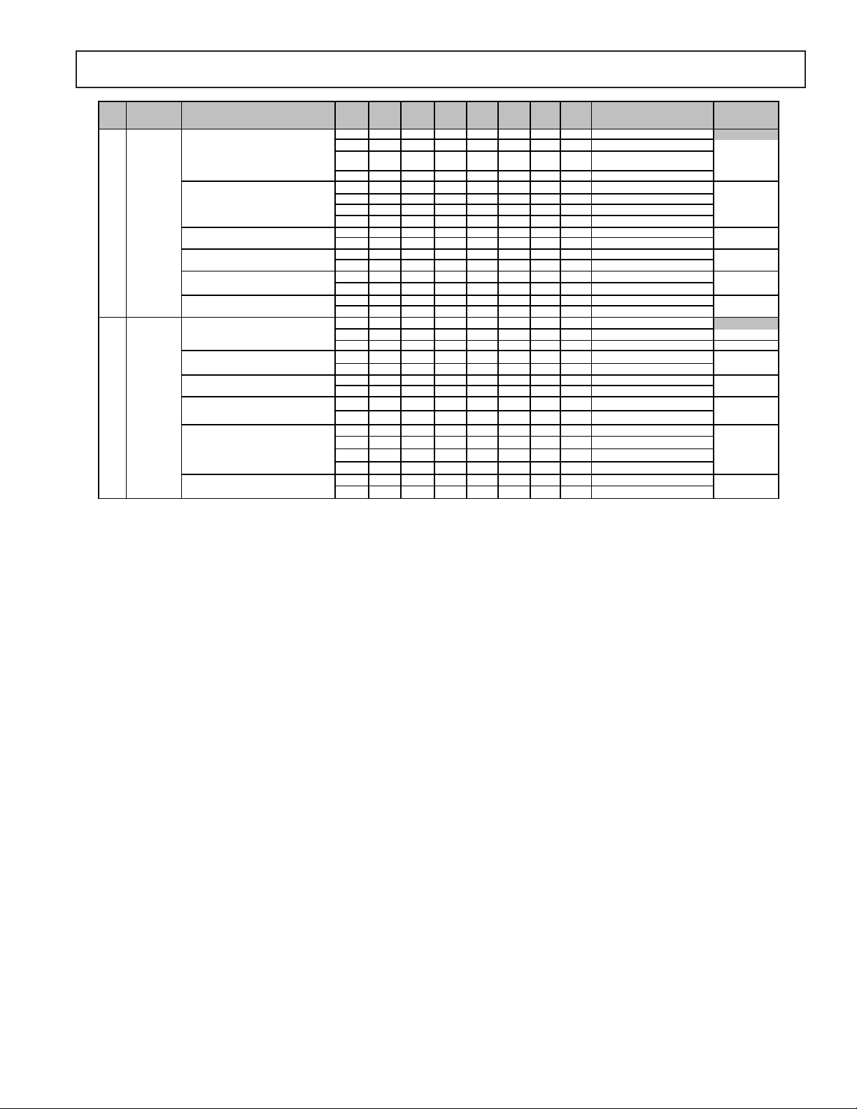
ADV7314
g
,
y
g
isabled
d
HD Sh
Fil
Disabled
SR7SR0 Register Bit Description Bit 7 Bit 6 Bit 5 Bit 4 Bit 3 Bit 2 Bit 1 Bit 0 Register Setting
10h HD Output Standard 0 0 EIA770.2 output 00h
HD Mode
Register 1
HD Input Control Signals 0 0
HD 625p 0 525p
HD 720p 0 1080i
HD BLANK Polarit
HD Macrovision for 525p/625p 0 Macrovision off
11h HD Pixel Data Valid 0Pixel data valid off 00h
HD Mode
Register 2
HD Test Pattern Enable 0 HD test pattern off
HD Test Pattern Hatch/Field 0 Hatch
HD VBI Open 0 D
HD Undershoot Limiter 0 0 Disabled
arpness
ter 0
1Macrovision on
1 Enabled
1720p
0
1
01 –11 IRE
10 –6 IRE
11 –1.5 IRE
01 EAV/SAV codes
10 Async timing mode
11 Reserved
1625p
1Field/Frame
1 Enable
01 EIA770.1 output
10 Output levels for full input
11 Reserved
0Reserved
1 HD test pattern on
ran
e
VSYNC, BLANK
HSYNC
BLANK active hi
BLANK active low
1Pixel data valid on
h
Reset Values
REV. 0
–21–
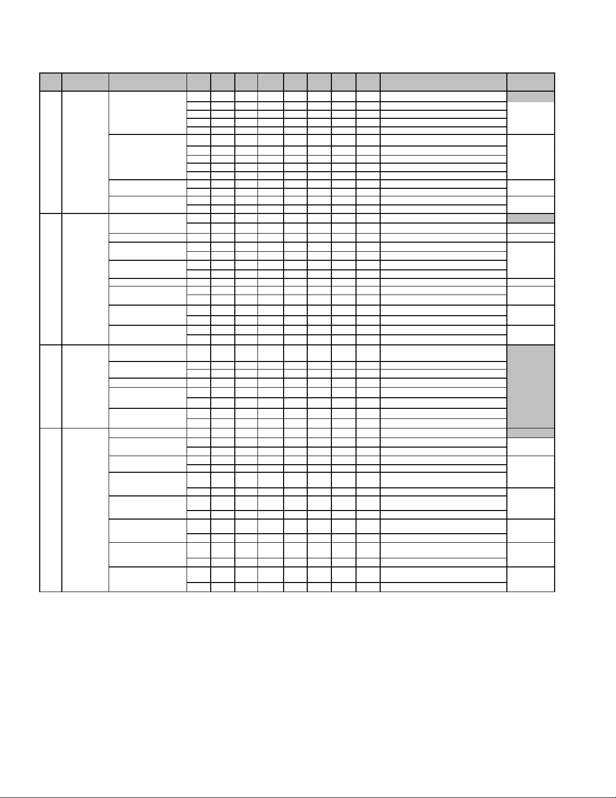
ADV7314
SR7SR0 Register Bit Description Bit 7 Bit 6 Bit 5 Bit 4 Bit 3 Bit 2 Bit 1 Bit 0 Register Setting
12h 0000 clk cycle 00h
HD Mode
Register 3
HD Mode
13h HD Cr/Cb Sequence 0
Register 4
14h HD Mode
Register 5
15h Reserved 0 0 must be written to this bit 00h
HD Mode
Register 6
NOTES
1
When set to 0, the line and field counters automatically wrap around at the end of the field/frame of the standard selected. When set to 1 , the field/line
HD Y Delay with
Respect to Falling Edge
of HSYNC
HD with Respect to
Falling Edge of HSYNC
HD CGMS 0 Disabled
HD CGMS CRC 0 Disabled
Reserved 0 0 must be written to this bit
HD Input Format
Sinc Filter on DAC D,
E, F
Reserved 0 0 must be written to this bit
HD Chroma SSAF 0 Disabled
HD Chroma Input 0 4:4:4
HD Double Buffering
HD Timing Reset x A low-high-low transition resets the
1080i Frame Rate 0 0 30 Hz/2200 total samples/line
Reserved 0 0 0 0 should be written to these bits
HD VSYNC/Field
Input
Lines/Frame
HD RGB Input 0 Disabled
HD Sync on PrPb 0 Disabled
HD Color DAC Swap 0 DAC E = Pb; DAC F = Pr
HD Gamma Curve A/B 0 Gamma Curve A
HD Gamma Curve
Enable
HD Adaptive Filter
Mode
HD Adaptive Filter
Enable
1
2
2
1 Enabled
0Disabled
1 Enabled
0 Update Field/line counter
1Field/line counter free running
0Disabled
1 Enabled
00 0 0 clk cycle
00 1 1 clk cycle
01 0 2 clk cycle
01 1 3 clk cycle
10 0 4 clk cycle
1 Enabled
1 Enabled
14:2:2
0Field Input
1
1 Gamma Curve B
0Disabled
1 Enabled
0 Mode A
1 Mode B
0011 clk cycle
0102 clk cycle
0113 clk cycle
1004 clk cycle
Cb after falling edge of HSYNC
1
Cr after falling edge of HSYNC
08-bit input
1 10-bit input
0Disabled
1 Enabled
internal HD timing counters
01 25 Hz/2640 total samples/line
VSYNC Input
1 Enabled
1 Enabled
1 DAC E = Pr; DAC F = Pb
counters are free running and wrap around when external sync signals indicate so.
2
Adaptive Filter mode is not available in PS only @ 54 MHz input mode.
Reset Value
4Ch
00h
REV. 0–22–
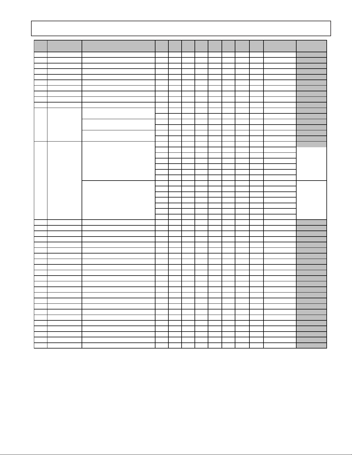
ADV7314
SR7SR0 Register Bit Description Bit 7 Bit 6 Bit 5 Bit 4 Bit 3 Bit 2 Bit 1 Bit 0
16h
HD Y Level
17h
HD Cr Level
18h
HD Cb Level
1
1
1
xxxxx xx x Y color value A0h
xxxxx xx x Cr color value 80 h
xxxxx xx x Cb color value 8 0 h
Register
Setting
Reset Value
19h Reserved 00h
1Ah Reserved 00h
1Bh Reserved 00h
1Ch Reserved 00h
1Dh Reserved 00h
1Eh Reserved 00h
1Fh Reserved 00h
15h HD Mode
Register 6
HD Gamma Curve Enable
HD Adaptive Filter Mode
0 Disabled
1 Enabled
0Mode A
1Mode B
HD Adaptive Filter Enable
0 Disabled
1 Enabled
20h 0000Gain A = 0 00 h
HD Sharpness
Filter Gain
HD Sharpness Filter Gain Value A
0001Gain A = +1
.. .. .. .. … …
0111Gain A = +7
100 0 Gain A = –8
.. .. .. .. … …
111 1 Gain A = –1
HD Sharpness Filter Gain Value B
0000 Gain B = 0
0001 Gain B = +1
.. .. .. .. …… .
0111 Gain B = +7
1000 Gain B = –8
.. .. .. .. …… ..
2
HD CGMS HD CGMS Data Bits 0000C19C18C17C16CGMS 19–16 00 h
21h
1111 Gain B = –1
22h HD CGMS HD CGMS Data Bits C15 C14 C13 C12 C 11 C10 C9 C8 CGMS 15–8 00h
23h HD CGMS HD CGMS Data Bits C7 C6 C5 C4 C3 C2 C1 C0 CGMS 7–0 00 h
24h
HD Gamma A
1
HD Gamma Curve A Data Points xxxxx xx x A0 00h
25h HD Gamma A HD Gamma Curve A Data Points xxxxx xx x A1 00h
26h HD Gamma A HD Gamma Curve A Data Points xxxxx xx x A2 00h
27h HD Gamma A HD Gamma Curve A Data Points xxxxx xx x A3 00h
28h HD Gamma A HD Gamma Curve A Data Points xxxxx xx x A4 00h
29h HD Gamma A HD Gamma Curve A Data Points xxxxx xx x A5 00h
2Ah HD Gamma A HD Gamma Curve A Data Points xxxxxxx x A6 00h
2Bh HD Gamma A HD Gamma Curve A Data Points xxxxxxx x A7 00h
2Ch HD Gamma A HD Gamma Curve A Data Points xxxxx xx x A8 00h
2Dh HD Gamma A HD Gamma Curve A Data Points xxxxx xx x A9 00h
2Eh HD Gamma B HD Gamma Curve B Data Points xxxxx xx x B0 00h
2Fh HD Gamma B HD Gamma Curve B Data Points xxxxx xx x B1 00h
30h HD Gamma B HD Gamma Curve B Data Points xxxxx xx x B2 00h
31h HD Gamma B HD Gamma Curve B Data Points xxxxx xx x B3 00h
32h HD Gamma B HD Gamma Curve B Data Points xxxxx xx x B4 00h
33h HD Gamma B HD Gamma Curve B Data Points xxxxx xx x B5 00h
34h HD Gamma B HD Gamma Curve B Data Points xxxxx xx x B6 00h
35h HD Gamma B HD Gamma Curve B Data Points xxxxx xx x B7 00h
36h HD Gamma B HD Gamma Curve B Data Points xxxxx xx x B8 00h
2
HD Gamma B HD Gamma Curve B Data Points xxxxx xx x B9 00h
37h
NOTES
1
Used for internal test pattern only.
2
Programmable gamma correction is not available in PS only mode @ 54 MHz operation.
REV. 0
–23–
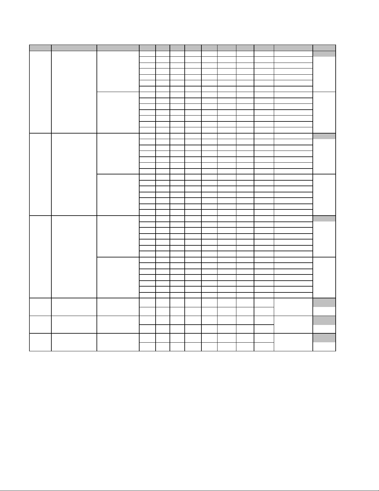
ADV7314
SR7–SR0 Register Bit Description Bit 7 Bit 6 Bit 5 Bit 4 Bit 3 Bit 2 Bit 1 Bit 0 Register Setting Value
38h HD Adaptive Filter 0 0 0 0 Gain A = 0 00h
39h 00 0 0 Gain A = 0 00h
3Ah 00 0 0 Gain A = 0 00h
3Bh
Gain 1 00 0 1 Gain A = +1
HD Adaptive Filter
Gain 2
HD Adaptive Filter
Gain 3
HD Adaptive Filter
Threshold A
HD Adaptive Filter
Gain 1 Value A
HD Adaptive Filter
Gain 1 Value B
HD Adaptive Filter
Gain 2 Value A
HD Adaptive Filter
Gain 2 Value B
HD Adaptive Filter
Gain 3 Value A
HD Adaptive Filter
Gain 3 Value B
HD Adaptive Filter
Threshold A Value
.. .. .. .. ……
01 1 1 Gain A = +7
10 0 0 Gain A = –8
.. .. .. .. ……
11 1 1 Gain A = –1
0000 Gain B = 0
0001 Gain B = +1
.. .. .. .. …….
0111 Gain B = +7
1000 Gain B = –8
.. .. .. .. ……..
1111 Gain B = –1
00 0 1 Gain A = +1
.. .. .. .. ……
01 1 1 Gain A = +7
10 0 0 Gain A = –8
.. .. .. .. ……
11 1 1 Gain A = –1
0000 Gain B = 0
0001 Gain B = +1
.. .. .. .. …….
0111 Gain B = +7
1000 Gain B = –8
.. .. .. .. ……..
1111 Gain B = –1
00 0 1 Gain A = +1
.. .. .. .. ……
01 1 1 Gain A = +7
10 0 0 Gain A = –8
.. .. .. .. ……
11 1 1 Gain A = –1
0000 Gain B = 0
0001 Gain B = +1
.. .. .. .. …….
0111 Gain B = +7
1000 Gain B = –8
.. .. .. .. ……..
1111 Gain B = –1
xxxxxx x x Threshold A 00h
3Ch
3Dh
HD Adaptive Filter
Threshold B
HD Adaptive Filter
Threshold C
HD Adaptive Filter
Threshold B Value
HD Adaptive Filter
Threshold C Value
xxxxxx x x Threshold B 00h
xxxxxx x x Threshold C 00h
REV. 0–24–
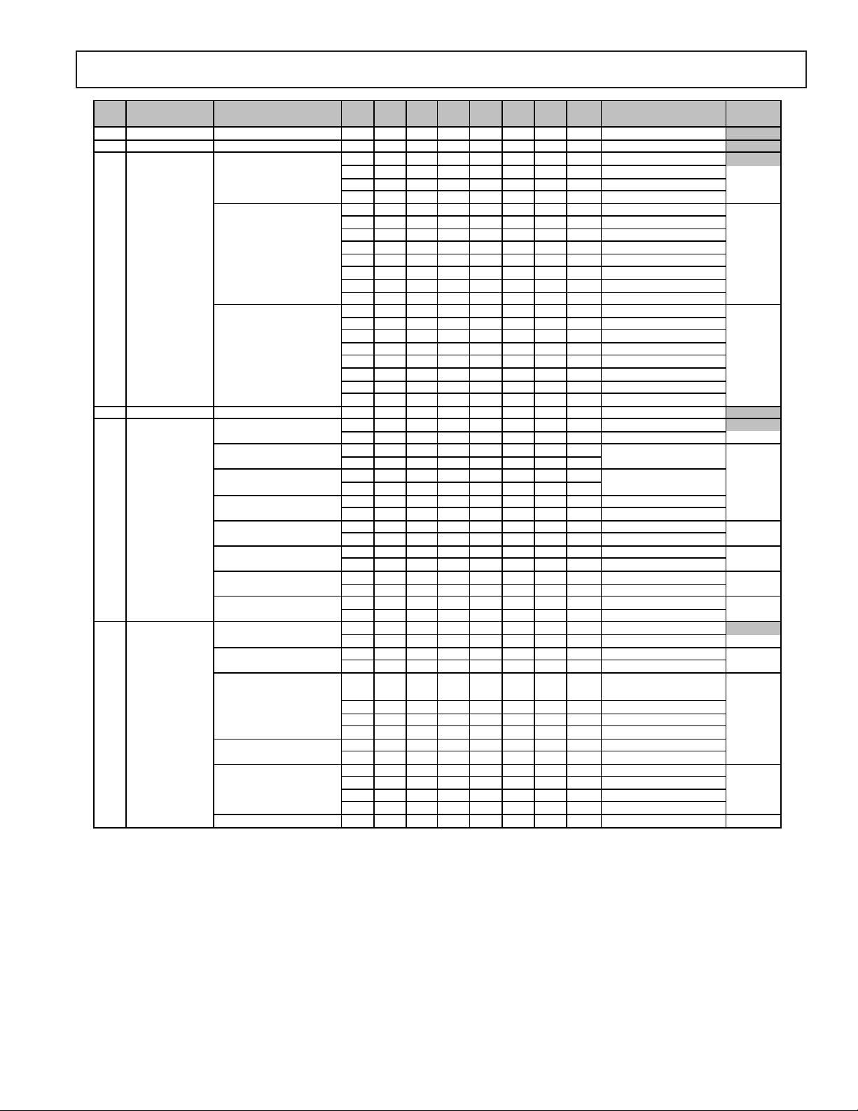
ADV7314
SR7–
SR0 Register Bit Description Bit 7 Bit 6 Bit 5 Bit 4 Bit 3 Bit 2 Bit 1 Bit 0
3Eh Reserved 00h
3Fh Reserved 00h
40h SD Mode Register 0 SD Standard 0 0
SD Luma Filter 0 0 0
SD Chroma Filter 0 0 0
41h Reserved 00h
42h SD Mode Register 1 SD UV SSAF 0
SD DAC Output 1 0
SD DAC Output 2 0
SD Pedestal 0
SD Square Pixel 0
SD VCR FF/RW Sync 0
SD Pixel Data Valid 0
SD SAV/EAV Step Edge
Control
43h SD Mode Register 2 SD Pedestal YPrPb Output 0
SD Output Levels Y 0
SD Output Levels PrPb 0 0
SD VBI Open 0
SD CC Field Control 0 0
Reserved 0 Reserved
001
010
011
100
101 Chroma CIF
110
111
1
0
1
01
10
11
00 1
01 0
01 1
10 0
10 1
11 0
11 1
1
1
1
01
10
11
1
01
10
11
1
1
1
Register Setting
NTSC
PAL B, D, G, H, I
PAL M
PAL N
LPF NTSC
LPF PAL
Notch NTSC
Notch PAL
SSAF Luma
Luma CIF
Luma QCIF
Reserved
1.3 MHz
0.65 MHz
1.0 MHz
2.0 MHz
Reserved
Chroma QCIF
3.0 MHz
Disabled
1
Enabled
Refer to Output
Configuration section
Refer to Output
Configuration section
Disabled
Enabled
Disabled
Enabled
Disabled
Enabled
Disabled
Enabled
Disabled
Enabled
No pedestal on YUV
1 7.5 IRE pedestal on YUV
Y = 700/300 mV
Y = 714/286 mV
700 mV p-p[PAL]; 1000 mV
p-p[NTSC]
700 mV p-p
1000 mV p-p
648 mV p-p
Disabled
Enabled
CC disabled
CC on odd field only
CC on even field only
CC on both fields
Reset
Value
00h
08h
00h
REV. 0
–25–
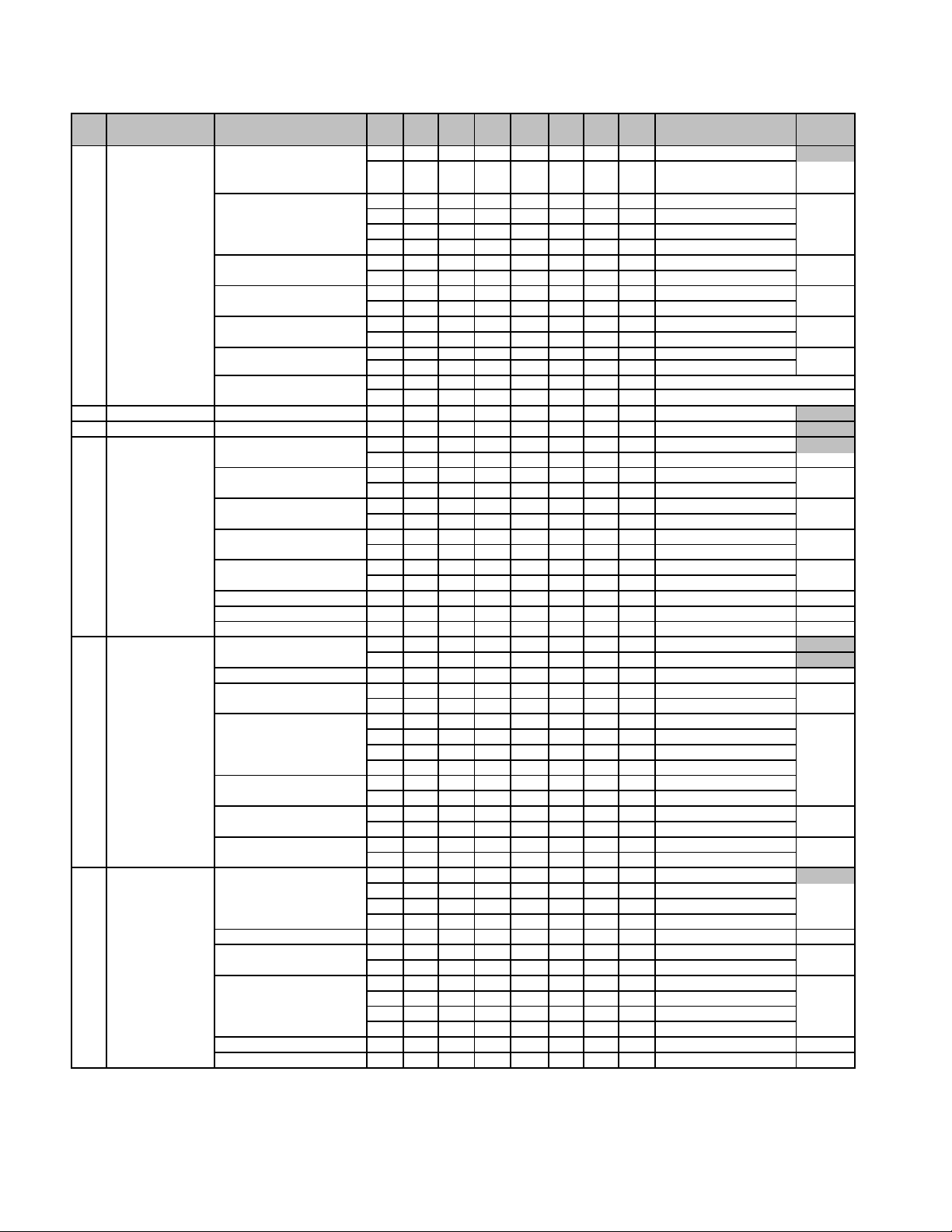
ADV7314
SR7–
SR0 Register Bit Description Bit 7 Bit 6 Bit 5 Bit 4 Bit 3 Bit 2 Bit 1 Bit 0 Register Setting
44h SD Mode Register SD VSYNC–3H 0 Disabled 0 0h
SD RTC/TR/SCR* 00 Genlock disabled
01 Subcarrier reset
10 Timing reset
11 RTC enabled
SD Active Video Length 0 720 pixels
1 710 [NTSC]/702 [PAL]
SD Chroma 0 Chroma enabled
1 Chroma disabled
SD Burst 0 Enabled
1 Disabled
SD Color Bars 0 Disabled
1 Enabled
SD DAC Swap 0
1
45h Reserved 00h
46h Reserved 00h
47h SD Mode Register SD PrPb Scale 0 Disabled 00h
SD Y Scale 0 Disabled
SD Hue Adjust 0 Disabled
1 Enabled
SD Brightness 0 Disabled
1 Enabled
SD Luma SSAF Gain 0 Disabled
1 Enabled
Reserved 0 0 must be written to
Reserved 0 0 must be written to
Reserved 0 0 must be written to
48h SD Mode Register Reserved 00h
1
VSYNC = 2.5 lines [PAL]
VSYNC = 3 lines [NTSC]
DAC B = Luma, DAC C = Chroma
DAC B = Chroma, DAC C = Luma
1 Enabled
1 Enabled
Reset
Value
Reserved 0 0 must be written to
SD Double Buffering 0 Disabled
SD Input Format 0 0 8-bit input
01 16-bit input
10 10-bit input
11 20-bit input
SD Digital Noise 0 Disabled
1 Enabled
SD Gamma Control 0 Disabled
1 Enabled
SD Gamma Curve 0 Gamma Curve A
1 Gamma Curve B
49h SD Mode Register SD Undershoot Limiter 0 0 Disabled 00h
Reserved 0 0 must be written to
SD Black Burst Output 0 Disabled
SD Chroma Delay 0 0 Disabled
01 4 clk cycles
10 8 clk cycles
11 Reserved
Reserved 0 0 must be written to
Reserved 0 0 must be written to
1 Enabled
01 –11 IRE
10 –6 IRE
11 –1.5 IRE
1 Enabled
*See Figure 31, RTC Timing and Connections.
REV. 0–26–
 Loading...