

Analog Devices ADV7202 Datasheet
PRELIMINARY TECHNICAL DATA
Simultaneous Sampling
a
Preliminary Technical Data
FEATURES
Four 10-Bit Video DACs (4:2:2, YCrCb, RGB I/P
Supported)
10-Bit Video Rate Digitization at Up to 54 Mhz
AGC Control (ⴞ6 dB)
Front-End 3-Channel Clamp Control
Up to Five CVBS Input Channels, Two Component YUV,
Three S-Video, or a combination of the above. Simul-
taneous Digitization of Two CVBS Input Channels.
Aux 8-Bit SAR ADC @ 843 kHz Sampling Giving up to
Eight General Purpose Inputs
2
C and SPI Compatible Interface with I2C Filter
I
RGB Inputs for Picture-on-Picture of the RGB DACs
APPLICATIONS
Picture-on-Picture Video Systems
Simultaneous Video Rate Processing
Hybrid Set-Top Box TV Systems
Direct Digital Synthesis/I-Q Demodulation
Image Processing
Video Rate Codec
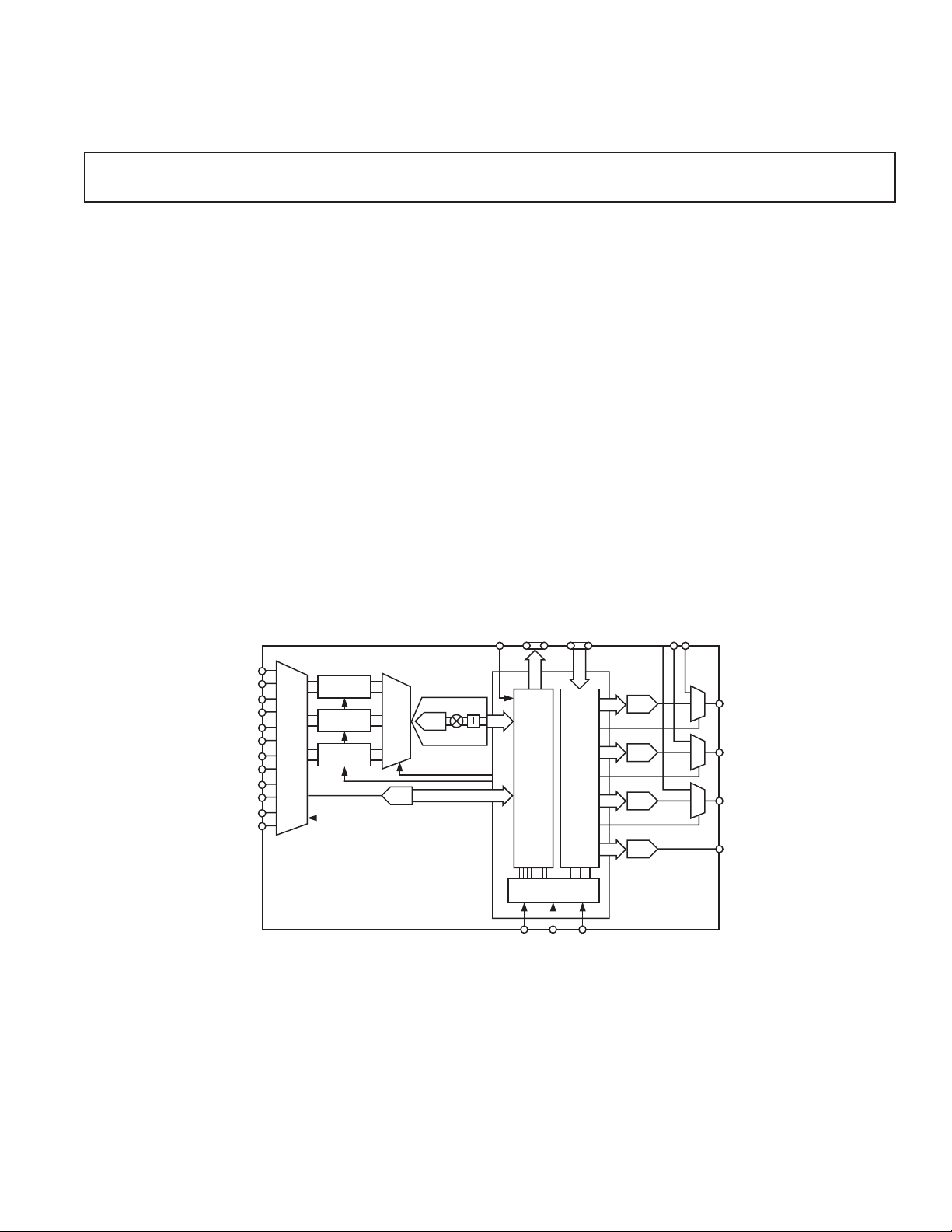
ADV7202
GENERAL DESCRIPTION
The ADV7202 is a video rate sampling Codec.
It has the capability of sampling up to five NTSC/PAL/SECAM
video I/P signals. The resolution on the front-end digitizer is
12 bits; 2 bits (12 dB) are used for gain and offset adjustment.
The digitizer has a conversion rate of 54 MHz.
It also has up to eight auxiliary inputs that can be sampled by
an 843 kHz SAR ADC for system monitoring, etc.
The back end consists of four 10-bit DACs that run at up to
54 MHz and can be used to output CVBS, S-Video, Component
YCrCb, and RGB.
This Codec also supports Picture-on-Picture with the 3-channel
I/P mux that also muxes to the DAC O/Ps.
The ADV7202 can operate at 3.3 V or 5 V. Its monolithic CMOS
construction ensures greater functionality with lower power
dissipation.
The ADV7202 is packaged in a small 64-lead LQFP package.
AIN1P
AIN1M
AIN2P
AIN2M
AIN3P
AIN3M
AIN4P
AIN4M
AIN5P
AIN5M
AIN6P
AIN6M
I/P
MUX
SHA AND
CLAMP
SHA AND
CLAMP
SHA AND
CLAMP
8-BIT 843KHz
ADV7202
FUNCTIONAL BLOCK DIAGRAM
DOUT
DAC DATA
[9:0]
12C/SPI
[9:0]
DAC
LOGIC
MUX
A/D
ADC BLOCK
12-BIT
A/D
XTAL
ADC
LOGIC
10-BIT
D/A
10-BIT
D/A
10-BIT
D/A
10-BIT
D/A
OSD I/P "S"
DAC0
DAC1
DAC2
DAC3
REV. PrB
Information furnished by Analog Devices is believed to be accurate and
reliable. However, no responsibility is assumed by Analog Devices for its
use, nor for any infringements of patents or other rights of third parties that
may result from its use. No license is granted by implication or otherwise
under any patent or patent rights of Analog Devices.
One Technology Way, P.O. Box 9106, Norwood, MA 02062-9106, U.S.A.
Tel: 781/329-4700 www.analog.com
Fax: 781/326-8703 © Analog Devices, Inc., 2002

PRELIMINARY TECHNICAL DATA
ADV7202–SPECIFICATIONS
5 V SPECIFICATIONS
(AVDD/DVDD = 5 V ⴞ 5%, V
= 1.235 V R
REF
= 1.2 k⍀, all specifications T
SET
MIN
1
to T
unless otherwise noted.)
MAX
Parameter Min Typ Max Unit Test Conditions
STATIC PERFORMANCE
Resolution (Each DAC) 10 Bits
Accuracy (Each DAC) 10
Integral Nonlinearity ± 2 LSB 10-Bit Operation
Differential Nonlinearity ± 2 LSB 10-Bit Operation
VIDEO ADC
Resolution 10 Bits (plus 2-Bits for gain ranging) 2.2 V Ref.
Accuracy 10
Integral Nonlinearity ± 1 LSB 10-Bit
Differential Nonlinearity ± 0.25 LSB 10-Bit
Input Voltage Range
SNR 62 dB 27 MHz Clock, f
2
–V
REFADC
+V
REFADC
See Figure TBD
= 100 kHz
IN
50 dB 54 MHz Clock, fIN = 100 kHz
AUX ADC
Resolution 8 Bits
Differential Nonlinearity ± 1 LSB Guaranteed Monotonic
Integral Nonlinearity ± 2 LSB
SNR 44 dB 27 MHz Clock
Input Voltage Range 0 2 V
REFADC
V
DIGITAL INPUTS
Input High Voltage, V
Input Low Voltage, V
Input Current, I
Input Capacitance, C
INL
IN
IN
INH
2V
0.8 V
± 1 µA
TBD pF
DIGITAL OUTPUTS
Output High Voltage, V
Output Low Voltage, V
OL
OH
2.4 V I
0.4 V I
SOURCE
= 3.2 mA
SINK
= 400 µA
Three-State Leakage Current 10 µA
Output Capacitance 10 pF
Digital Output Access Time, t
Digital Output Hold Time, t
14
15
8 ns See Figure 16
3ns
ANALOG OUTPUTS
Output Current 4.33 mA R
= 1.2 kΩ, RL = 300 Ω
SET
DAC-to-DAC Matching 2 %
Output Compliance, V
Output Impedance, R
Output Capacitance, C
Analog Output Delay
OC
OUT
3
OUT
0 +1.4 V
50 kΩ
30 pF I
7ns
OUT
= 0 mA
DAC Output Skew 0 ns
VOLTAGE REFERENCE
Reference Range, V
Reference Range, V
Reference Range, V
NOTES
1
0°C to 70°C
2
SHA gain = 1, half range for SHA gain = 2, see Table II.
3
Output Delay measured from 50% of the rising edge of the clock to the 50% point of full-scale transition.
Specifications subject to change without notice.
REFDAC
REFADC
REFADC
1.235 V
2.200 V Programmable 1.1 V or 2.2 V
1.100 V
–2–
REV. PrB

PRELIMINARY TECHNICAL DATA
ADV7202
5 V SPECIFICATIONS
(AVDD/DVDD = 5 V ⴞ 5%, V
= 1.235 V R
REF
= 1.2 k⍀, all specifications T
SET
MIN
to T
unless otherwise noted.)
MAX
Parameter Min Typ Max Unit Test Conditions
POWER REQUIREMENTS
1
AVDD/DVDD 4.75 5 5.25 V
Normal Power Mode
I
DAC
I
DSC
I
ADC
2
3
4
4mAR
= 1.2 kΩ, RL = 300 Ω
SET
34 mA
21 mA
Sleep Mode
Current 100 µAR
= 1.2 kΩ, RL = 300 Ω
SET
PSU Rejection Ratio
DACs 0.01 0.5 %/% COMP = 0.1 µF
Video ADC 0.01 0.5 %/%
Aux ADC TBD TBD TBD TBD
Power-Up Time TBD TBD Ref. power-up time
MPU PORT—I
2C5
SCLOCK Frequency 0 400 kHz
SCLOCK High Pulsewidth, t
SCLOCK Low Pulsewidth, t
1
2
Hold Time (Start Condition), t
0.6 µs
1.3 µs
0.6 µs After this period the first clock is
3
generated.
Setup Time (Start Condition), t
Data Setup Time, t
5
SDATA, SCLOCK Rise Time, t
SDATA, SCLOCK Fall Time, t
0.6 µs Relevant for Repeated Start Condition
4
100 ns
6
7
300 ns
300 ns
Setup Time (Stop Condition), t80.6 µs
MPU PORT—SPI
5, 6
SCLOCK Frequency 0 10 MHz
SCLOCK High Pulsewidth, t
SCLOCK Low Pulsewidth, t
SI Data Setup Time, t
SI Data Hold Time, t
19
21
22
20
TBD TBD kHz
TBD TBD ns
TBD TBD ns
TBD TBD ns
RESET Low Time 100 ns
NOTES
1
All DACs and ADCs on.
2
I
is the DAC supply current.
DAC
3
I
is the digital core supply current.
DSC
4
I
is the ADC supply current.
ADC
5
TTL input values are 0 V to 3 V, with input rise/fall times
Timing reference points at 50% for inputs and outputs.
6
See SPI timing diagram Figures 10 and 11.
Specifications subject to change without notice.
≤3 ns, as measured between the 10% and 90% points.
REV. PrB
–3–

PRELIMINARY TECHNICAL DATA
ADV7202–SPECIFICATIONS
5 V SPECIFICATIONS
(AVDD/DVDD = 4.75 – 5.25, V
= 1.235 V R
REF
= 1.2 k⍀, all specifications T
SET
MIN
Parameter Min Typ Max Unit Condition
1
to T
unless otherwise noted.)
MAX
2
PROGRAMMABLE GAIN
AMPLIFIER
Video ADC Gain –6 +6 dB Setup Conditions
CLAMP CIRCUITRY
3
Clamp Off Leakage Current TBD µA
Clamp Fine Source/Sink Current 3 µA
Clamp Coarse Source/Sink Current 0.5 mA
CLOCK CONTROL
DACCLK0/1
DACCLK1 80 MHz Single Edge Single Clock Mode
DACCLK1
8
Data Setup Time, t
Data Hold Time, t
Pipeline Delay
6, 7
4
27 MHz Dual CLK Dual Edge Mode
27 MHz 4:2:2 Mode
12
13
5
, t
18
2 ns All Input Modes
2ns
Video ADC TBD Clock Cycles
SAR TBD Clock Cycles
RESET CONTROL
RESET Low Time 10 ns
NOTES
1
Temperature range T
2
The max/min specifications are guaranteed over this range. The max/min values are typical over 4.75 V to 5.25 V range.
3
External clamp capacitor = 0.1 µF.
4
TTL input values are 0 V to 3 V, with input rise/fall times ≤3 ns, measured between the 10% and 90% points. Timing reference points at 50% for inputs and outputs.
Analog output load ≤10 pF.
5
Output delay measured from the 50% point of the rising edge of CLOCK to the 50% point of full scale transition.
6
Maximum clock speed determined by setup and hold conditions.
7
Single DAC only.
8
Guaranteed by Characterization.
Specifications subject to change without notice.
MIN
to T
: 0oC to 70oC.
MAX
–4–
REV. PrB

PRELIMINARY TECHNICAL DATA
ADV7202
3.3 V SPECIFICATIONS
(AVDD/DVDD = 3.3 V ⴞ 5%, V
= 1.235 V R
REF
= 1.2 k⍀, all specifications T
SET
MIN
1
to T
unless otherwise noted.)
MAX
Parameter Min Typ Max Unit Test Conditions
STATIC PERFORMANCE
Resolution (Each DAC) 10 Bits
Accuracy (Each DAC) 10
Integral Nonlinearity ± 2 LSB 10-Bit Operation
Differential Nonlinearity ± 2 LSB 10-Bit Operation
VIDEO ADC
Resolution 10 10 Bits (Plus 2-Bits for gain ranging) 2.2 V Ref.
Accuracy 10
Integral Nonlinearity ± 1 LSB 10-Bit
Differential Nonlinearity ± 0.25 LSB 10-Bit
Differential Input Voltage Range
SNR 62 dB 27 MHz Clock, f
2
–V
REFADC
+V
REFADC
See Table II
= 100 kHz
IN
50 dB 54 MHz Clock, fIN = 100 kHz
AUX ADC
Resolution Bits
Differential Nonlinearity ± 1 LSB Guaranteed Monotonic
Integral Nonlinearity ± 2 LSB
SNR 44 dB 27 MHz Clock
Input Voltage Range 0 2 V
REFADC
V
DIGITAL INPUTS
Input High Voltage, V
Input Low Voltage, V
Input Current, I
Input Capacitance, C
INL
IN
IN
INH
2V
0.8 V
± 1 µA
10 pF
DIGITAL OUTPUTS
Output High Voltage, V
Output Low Voltage, V
OL
OH
2.4 V I
0.4 V I
SOURCE
= 3.2 mA
SINK
= 400 µA
Three-State Leakage Current 10 µA
Output Capacitance 30 pF
Digital Output Access Time, t
Digital Output Hold Time, t
14
15
8 ns See Figure 16
3ns
ANALOG OUTPUTS
Output Current 4.33 mA R
DAC-to-DAC Matching 2 %
Output Compliance, V
Output Impedance, R
Output Capacitance, C
Analog Output Delay
OUT
3
OC
OUT
0 1.4 V
50 kΩ
30 pF I
7ns
DAC Output Skew 0 ns
VOLTAGE REFERENCE
Reference Range, V
Reference Range, V
NOTES
1
0°C to 70°C.
2
SHA gain = 1, half range for SHA gain = 2, see Table II.
3
Output delay measured from 50% of the rising edge of the clock to the 50% point of full scale transition.
Specifications subject to change without notice.
REFDAC
REFADC
1.235 V
1.100 V
= 1.2 kΩ, RL = 300 Ω
SET
= 0 mA
OUT
REV. PrB
–5–

PRELIMINARY TECHNICAL DATA
ADV7202–SPECIFICATIONS
3.3 V SPECIFICATIONS
(AVDD/DVDD = 3.3 V ⴞ 5%, V
= 1.235 V R
REF
= 1.2 k⍀, all specifications T
SET
MIN
to T
MAX
Parameter Min Typ Max Unit Test Conditions
POWER REQUIREMENTS
1
AVDD/DVDD 3.15 3.3 3.45 V
Normal Power Mode
I
DAC
I
DSC
I
ADC
2
3
4
4mAR
= 1.2 kΩ, RL = 300 Ω
SET
34 mA
21 mA
Sleep Mode
Current 100 µAR
= 1.2 kΩ, RL = 300 Ω
SET
PSU Rejection Ratio
DACs 0.01 0.5 %/% COMP = 0.1 µF
Video ADC 0.01 0.5 %/%
Aux ADC TBD TBD TBD TBD
Power-Up Time TBD TBD TBD
MPU PORT—I
2C5
SCLOCK Frequency 0 400 kHz
SCLOCK High Pulsewidth, t
SCLOCK Low Pulsewidth, t
1
2
Hold Time (Start Condition), t
0.6 µs
1.3 µs
0.6 µs After this period the first clock is
3
generated.
Setup Time (Start Condition), t
Data Setup Time, t
5
SDATA, SCLOCK Rise Time, t
SDATA, SCLOCK Fall Time, t
0.6 µs Relevant for Repeated Start Condition
4
100 ns
6
7
300 ns
300 ns
Setup Time (Stop Condition), t80.6 µs
MPU PORT—SPI
5, 6
SCLOCK Frequency TBD TBD kHz
SCLOCK High Pulsewidth, t
SCLOCK Low Pulsewidth, t
SI Data Setup Time, t
SI Data Hold Time, t
19
21
22
20
TBD TBD kHz
TBD TBD ns
TBD TBD ns
TBD TBD ns
RESET Low Time 100 ns
NOTES
1
All DACs and ADCs on.
2
I
is the DAC supply current.
DAC
3
I
is the digital core supply current.
DSC
4
I
is the ADC supply current.
ADC
5
TTL input values are 0 V to 3 V, with input rise/fall times
6
See SPI timing diagram Figures 10 and 11.
Specifications subject to change without notice.
≤ 3 ns, as measured between the 10% and 90% points. Timing reference points at 50% for inputs and outputs.
unless otherwise noted.)
–6–
REV. PrB

PRELIMINARY TECHNICAL DATA
ADV7202
3.3 V SPECIFICATIONS
(AVDD/DVDD = 3.3 V ⴞ 5%, V
= 1.235 V R
REF
= 1.2 k⍀, all specifications T
SET
MIN
Parameter Min Typ Max Unit Condition
1
to T
unless otherwise noted.)
MAX
2
PROGRAMMABLE GAIN
AMPLIFIER
Video ADC Gain –6 +6 dB Setup Conditions
CLAMP CIRCUITRY
3
Clamp Off Leakage Current TBD µA
Clamp Fine Source/Sink Current 3 µA
Clamp Coarse Source/Sink Current 0.5 mA
CLOCK CONTROL
4
DACCLK0/1 27 MHz Dual CLK Dual Edge Mode
DACCLK1 54 MHz Single Edge Dual Clock Mode
DACCLK1 27 MHz 4 : 2 : 2 Mode
Clock High Time, t
Clock Low Time, t
Clock High Time, t
Clock Low Time, t
Data Setup Time, t
Data Hold Time, t
Pipeline Delay
(DACCLK0) 18 ns Dual Edge Dual Clock Mode
10
(DACCLK0) 18 ns
11
(DACCLK1) 18 ns
10
(DACCLK1) 18 ns
11
12
13
5
, t
18
2 ns All Input Modes
2ns
Video ADC TBD Clock Cycles
SAR TBD Clock Cycles
RESET CONTROL
RESET Low Time 10 ns
NOTES
1
Temperature range T
2
The max/min specifications are guaranteed over this range. The max/min values are typical over 3.15 V to 3.45 V range.
3
External clamp capacitor = 0.1 µF.
4
TTL input values are 0 V to 3 V, with input rise/fall times ≤3 ns, measured between the 10% and 90% points. Timing reference points at 50% for inputs and outputs.
Analog output load ≤10 pF.
5
Output delay measured from the 50% point of the rising edge of CLOCK to the 50% point of full-scale transition.
Specifications subject to change without notice.
MIN
to T
: 0oC to 70oC.
MAX
REV. PrB
–7–
ADV7202
WARNING!
ESD SENSITIVE DEVICE
PRELIMINARY TECHNICAL DATA
ABSOLUTE MAXIMUM RATINGS
1
AVDD to AVSS . . . . . . . . . . . . . . . . . . . . . . . . . . . . . . . . . 7 V
DVDD to DVSS . . . . . . . . . . . . . . . . . . . . . . . . . . . . . . . . 7 V
Ambient Operating Temperature (T
Storage Temperature (T
Junction Temperature (T
) . . . . . . . . . . . . . . –65°C to +150°C
S
) . . . . . . . . . . . . . . . . . . . . . 150°C
J
) . . . . . . . . 0°C to 70°C
A
Lead Temperature (Soldering, 10 secs) . . . . . . . . . . . . 300°C
Vapor Phase Soldering (1 minute) . . . . . . . . . . . . . . . . 220°C
to GND2 . . . . . . . . . . . . . . . . . . . . . . . . . . . . 0 V to V
I
OUT
NOTES
1
Stresses above those listed under Absolute Maximum Ratings may cause perma-
AA
nent damage to the device. This is a stress rating only; functional operation of the
device at these or any other conditions above those listed in the operational
sections of this specification is not implied. Exposure to absolute maximum rating
conditions for extended periods may affect device reliability.
2
Analog output short circuit to any power supply or common can be of an indefinite
duration.
ORDERING INFORMATION
1
Model Temperature Range Package Description Package Option
ADV7202 0°C to 70°C 64-Lead Plastic Quad Flatpack (LQFP) ST-64
CAUTION
ESD (electrostatic discharge) sensitive device. Electrostatic charges as high as 4000 V readily
accumulate on the human body and test equipment and can discharge without detection. Although
the ADV7202 features proprietary ESD protection circuitry, permanent damage may occur on
devices subjected to high-energy electrostatic discharges. Therefore, proper ESD precautions are
recommended to avoid performance degradation or loss of functionality.
SYNC_IN
CLK/SCK
LE/ALSB
XTAL0
XTAL1
AVDD_ADC
AVSS_ADC
AIN1P
AIN1M
AIN2P
AIN12M
AIN3P
AIN3M
AIN4P
AIN4M
AIN5P
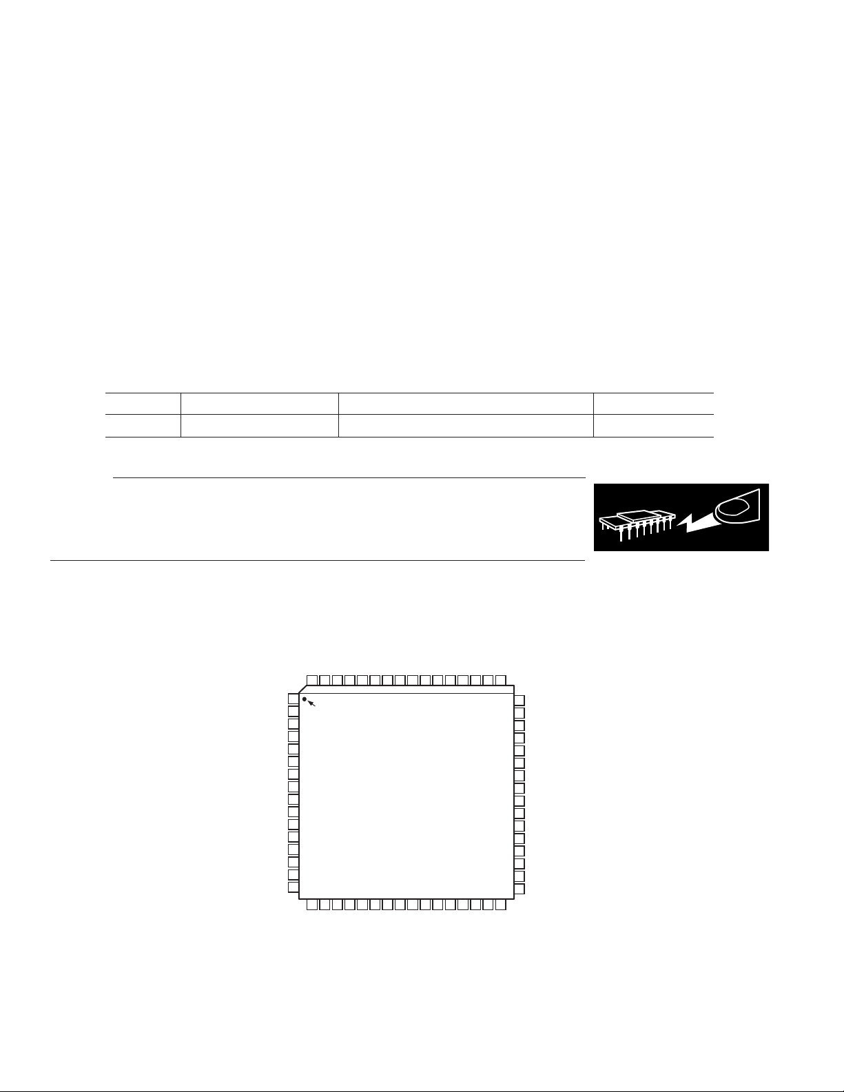
PIN CONFIGURATION
SYNC_OUT
DAC_DATA0
DAC_DATA1
DAC_DATA2
DAC_DATA3
DACCLK0
DACCLK1
DAC_DATA4
DAC_DATA5
CAP1
DOUT9
OSDEN
DVDD
DVSS
DOUT8
DOUT7
SI_DATA9
64 63 62 61 60 55 54 53 52 51 50 4959 58 57 56
1
PIN 1
2
IDENTIFIER
3
4
5
6
7
8
9
10
11
12
13
14
15
16
17 18 19 20 21 22 23 24 25 26 27 28 29 30 31 32
AIN6P
AIN5M
AIN6M
SPI_SEL
REFADC
ADV7202
TOP VIEW
(Not to Scale)
CML
CAP2
DAC_DATA6
DAC_DATA7
DAC_DATA8
DAC_DATA9
DOUT6
DOUT5
DOUT3
DOUT4
48
RESET
47
RSET
46
VREFDAC
45
COMP
44
DAC0_OUT
43
DAC1_OUT
42
AVSDD_DAC
41
AVSS_DAC
40
DAC2_OUT
39
DAC3_OUT
38
OSDIN0
37
OSDIN1
36
OSDIN2
35
DOUT0
34
DOUT1
33
DOUT2
–8–
REV. PrB
 Loading...