Analog Devices ADV7178, ADV7177 Datasheet
Integrated Digital CCIR-601
a
FEATURES
ITU-R BT601/656 YCrCb to PAL/NTSC Video Encoder
High Quality 9-Bit Video DACs
Integral Nonlinearity <1 LSB at 9 Bits
NTSC-M, PAL-M/N, PAL-B/D/G/H/I
Single 27 MHz Crystal/Clock Required (ⴛ2 Oversampling)
75 dB Video SNR
32-Bit Direct Digital Synthesizer for Color Subcarrier
Multistandard Video Output Support:
Composite (CVBS)
Component S-Video (Y/C)
Component YUV and RGB
Video Input Data Port Supports:
CCIR-656 4:2:2 8-Bit Parallel Input Format
4:2:2 16-Bit Parallel Input Format
SMPTE 170M NTSC-Compatible Composite Video
ITU-R BT.470 PAL-Compatible Composite Video
Full Video Output Drive or Low Signal Drive Capability
34.7 mA max into 37.5 ⍀ (Doubly-Terminated 75R)
5 mA min with External Buffers
Programmable Simultaneous Composite and S-VHS
(VHS) Y/C or RGB (SCART)/YUV Video Outputs
Programmable Luma Filters (Low-Pass/Notch/Extended)
Programmable VBI (Vertical Blanking Interval)
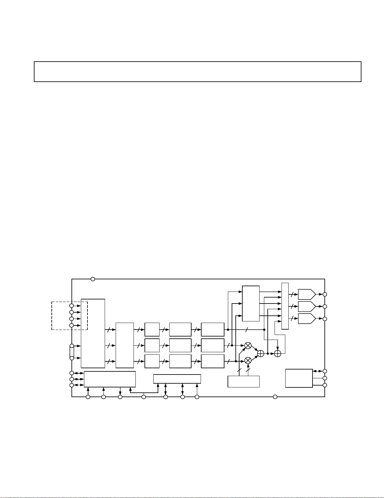
FUNCTIONAL BLOCK DIAGRAM
V
AA
to PAL/NTSC Video Encoder
ADV7177/ADV7178
Programmable Subcarrier Frequency and Phase
Programmable LUMA Delay
Individual ON/OFF Control of Each DAC
CCIR and Square Pixel Operation
Color Signal Control/Burst Signal Control
Interlaced/Noninterlaced Operation
Complete On-Chip Video Timing Generator
OSD Support (AD7177 Only)
Programmable Multimode Master/Slave Operation
Macrovision Antitaping Rev 7.01 (ADV7178 Only)**
Closed Captioning Support
Onboard Voltage Reference
2-Wire Serial MPU Interface (I
Single Supply +5 V or +3 V Operation
Small 44-Lead PQFP Package
Synchronous 27 MHz/13.5 MHz Clock O/P
APPLICATIONS
MPEG-1 and MPEG-2 Video, DVD, Digital Satellite/
Cable Systems (Set Top Boxes/IRDs), Digital TVs,
CD Video/Karaoke, Video Games, PC Video/Multimedia
GENERAL DESCRIPTION
The ADV7177/ADV7178 is an integrated digital video encoder
that converts Digital CCIR-601 4:2:2 8- or 16-bit component
video data into a standard analog baseband television signal
2C®
Compatible)
(Continued on page 11)
M
U
ADV7177
ONLY
OSD_EN
OSD_0
OSD_1
OSD_2
COLOR
DATA
P7–P0
P15–P8
HSYNC
FIELD/VSYNC
BLANK
*Protected by U.S. Patent Numbers 5,343,196 and 5,442,355 and other intellectual property rights.
**This device is protected by U.S. Patent Numbers 4,631,603, 4,577,216, 4,819,098 and other intellectual property rights. The Macrovision anticopy process is
licensed for noncommercial home use only, which is its sole intended use in the device. Please contact sales office for latest Macrovision version available.
NOTE: ITU-R and CCIR are used interchangeably in this document (ITU-R has replaced CCIR recommendations).
2
I
C is a registered trademark of Philips Corporation.
4:2:2 TO
4:4:4
INTER-
POLATOR
CLOCK
VIDEO TIMING
GENERATOR
CLOCK
ADV7177/ADV7178
8
YCrCb
8
TO
YUV
MATRIX
8 8
CLOCK/2
8
8
RESET
YUV TO
RBG
MATRIX
8
ADD
SYNC
ADD
BURST
ADD
BURST
INTER-
POLATOR
8
INTER-
POLATOR
8
INTER-
POLATOR
I2C MPU PORT
SCLOCK SDATA ALSB GND
8
8
8
Y
LOW-PASS
FILTER
U
LOW-PASS
FILTER
V
LOW-PASS
FILTER
9
9
SIN/COS
DDS BLOCK
9
99
9
L
T
I
9
P
L
E
9
X
E
R
VOLTAGE
REFERENCE
CIRCUIT
9-BIT
DAC
9-BIT
DAC
9-BIT
DAC
DAC A (PIN 31)
DAC B (PIN 27)
DAC C (PIN 26)
V
REF
R
SET
COMP
REV. 0
Information furnished by Analog Devices is believed to be accurate and
reliable. However, no responsibility is assumed by Analog Devices for its
use, nor for any infringements of patents or other rights of third parties
which may result from its use. No license is granted by implication or
otherwise under any patent or patent rights of Analog Devices.
One Technology Way, P.O. Box 9106, Norwood, MA 02062-9106, U.S.A.
Tel: 781/329-4700 World Wide Web Site: http://www.analog.com
Fax: 781/326-8703 © Analog Devices, Inc., 1998

ADV7177/ADV7178–SPECIFICATIONS
5 V SPECIFICATIONS
(VAA = +5 V ⴞ 5%1, V
Parameter Conditions
STATIC PERFORMANCE
3
= 1.235 V, R
REF
1
= 300 ⍀. All specifications T
SET
Min Typ Max Units
MIN
Resolution (Each DAC) 9 Bits
Accuracy (Each DAC)
Integral Nonlinearity ±1.0 LSB
Differential Nonlinearity Guaranteed Monotonic ±1.0 LSB
DIGITAL INPUTS
Input High Voltage, V
Input Low Voltage, V
Input Current, I
Input Current, I
Input Capacitance, C
DIGITAL OUTPUTS
Output High Voltage, V
Output Low Voltage, V
3
INH
INL
4
IN
5
IN
IN
3
OH
OL
V
= 0.4 V or 2.4 V ±1 µA
IN
V
= 0.4 V or 2.4 V ±50 µA
IN
I
I
= 400 µA 2.4 V
SOURCE
= 3.2 mA 0.4 V
SINK
2V
Three-State Leakage Current 10 µA
Three-State Output Capacitance 10 pF
ANALOG OUTPUTS
Output Current
Output Current
3
6
7
R
= 300 Ω, RL = 75 Ω 16.5 17.35 18.5 mA
SET
DAC-to-DAC Matching 0.6 5 %
Output Compliance, V
Output Impedance, R
Output Capacitance, C
VOLTAGE REFERENCE
Reference Range, V
POWER REQUIREMENTS
V
AA
Low Power Mode
I
DAC
I
DAC
I
CCT
(max)
(min)
10
9
9
OC
OUT
OUT
3
REF
3, 8
I
= 0 mA 30 pF
OUT
I
VREFOUT
= 20 µA 1.112 1.235 1.359 V
0 +1.4 V
4.75 5.0 5.25 V
Power Supply Rejection Ratio COMP = 0.1 µF 0.01 0.5 %/%
NOTES
11
The max/min specifications are guaranteed over this range. The max/min values are typical over 4.75 V to 5.25 V.
12
Temperature range T
13
Guaranteed by characterization.
14
All digital input pins except pins RESET, OSD0 and CLOCK.
15
Excluding all digital input pins except pins RESET, OSD0 and CLOCK.
16
Full
drive into 75␣ Ω load.
17
Minimum drive current (used with buffered/scaled output load).
18
Power measurements are taken with Clock Frequency = 27 MHz. Max T
19
I
is the total current (min corresponds to 5 mA output per DAC, max corresponds to 18.5 mA output per DAC) to drive all three DACs. Turning off individual
DAC
DACs reduces I
10
I
(Circuit Current) is the continuous current required to drive the device.
CCT
Specifications subject to change without notice.
to T
MIN
correspondingly.
DAC
: 0°C to +70°C.
MAX
= 110°C.
J
2
to T
unless otherwise noted.)
MAX
0.8 V
10 pF
5mA
15 kΩ
62 mA
25 mA
100 150 mA
–2–
REV. 0

ADV7177/ADV7178
3.3 V SPECIFICATIONS
(VAA = +3.0 V–3.6 V1, V
REF
Parameter Conditions
STATIC PERFORMANCE
3
= 1.235 V, R
1
= 300 ⍀. All specifications T
SET
Min Typ Max Units
MIN
2
to T
unless otherwise noted.)
MAX
Resolution (Each DAC) 9 Bits
Accuracy (Each DAC)
Integral Nonlinearity ±0.5 LSB
Differential Nonlinearity Guaranteed Monotonic ±0.5 LSB
DIGITAL INPUTS
Input High Voltage, V
Input Low Voltage, V
Input Current, I
Input Current, I
Input Capacitance, C
IN
IN3,
3, 4
INL
5
IN
INH
V
= 0.4 V or 2.4 V ±1 µA
IN
V
= 0.4 V or 2.4 V ±50 µA
IN
2V
0.8 V
10 pF
DIGITAL OUTPUTS
Output High Voltage, V
Output Low Voltage, V
OH
OL
Three-State Leakage Current
Three-State Output Capacitance
ANALOG OUTPUTS
Output Current
Output Current
3
6, 7
8
3
3
I
I
= 400 µA 2.4 V
SOURCE
= 3.2 mA 0.4 V
SINK
10 µA
10 pF
R
= 300 Ω, RL = 75 Ω 16.5 17.35 18.5 mA
SET
5mA
DAC-to-DAC Matching 2.0 %
Output Compliance, V
Output Impedance, R
Output Capacitance, C
POWER REQUIREMENTS
V
AA
Normal Power Mode
I
DAC
I
DAC
I
CCT
Low Power Mode
I
DAC
I
DAC
I
CCT
(max)
(min)
9
(max)
(min)
11
10
10
10
10
OC
OUT
OUT
3, 9
I
= 0 mA 30 pF
OUT
R
= 300 Ω, RL = 150 Ω 113 116 mA
SET
0 +1.4 V
15 kΩ
3.0 3.3 3.6 V
15 mA
45 mA
60 mA
25 mA
45 mA
Power Supply Rejection Ratio COMP = 0.1 µF 0.01 0.5 %/%
NOTES
11
The max/min specifications are guaranteed over this range. The max/min values are typical over 3.0 V to 3.6 V.
12
Temperature range T
13
Guaranteed by characterization.
14
All digital input pins except pins RESET, OSD0 and CLOCK.
15
Excluding all digital input pins except pins RESET, OSD0 and CLOCK.
16
Full
drive into 75␣ Ω load.
17
DACs can output 35 mA typically at 3.3 V (R
18
Minimum drive current (used with buffered/scaled output load).
19
Power measurements are taken with Clock Frequency = 27 MHz. Max T
10
I
is the total current (min corresponds to 5 mA output per DAC, max corresponds to 38 mA output per DAC) to drive all three DACs. Turning off individual
DAC
DACs reduces I
11
I
(Circuit Current) is the continuous current required to drive the device.
CCT
Specifications subject to change without notice.
to T
MIN
correspondingly.
DAC
: 0°C to +70°C.
MAX
= 150 Ω and RL = 75 Ω), optimum performance obtained at 18 mA DAC current (R
SET
= 110°C.
J
= 300 Ω and RL = 150 Ω).
SET
–3–REV. 0

ADV7177/ADV7178–SPECIFICATIONS
(VAA = +4.75 V – 5.25 V1, V
5 V DYNAMIC SPECIFICATIONS
Parameter Conditions
1
unless otherwise noted.)
1
Filter Characteristics
Luma Bandwidth3 (Low-Pass Filter) NTSC Mode
Stopband Cutoff >54 dB Attenuation 7.0 MHz
Passband Cutoff F
3 dB
>3 dB Attenuation 4.2 MHz
Chroma Bandwidth NTSC Mode
Stopband Cutoff >40 dB Attenuation 3.2 MHz
Passband Cutoff F
Luma Bandwidth
3 dB
3
(Low-Pass Filter) PAL MODE
>3 dB Attenuation 2.0 MHz
Stopband Cutoff >50 dB Attenuation 7.4 MHz
Passband Cutoff F
3 dB
>3 dB Attenuation 5.0 MHz
Chroma Bandwidth PAL MODE
Stopband Cutoff >40 dB Attenuation 4.0 MHz
Passband Cutoff F
Differential Gain
Differential Phase
4
SNR
(Pedestal) RMS 75 dB rms
4
(Ramp) RMS 57 dB rms
SNR
Hue Accuracy
Color Saturation Accuracy
Chroma Nonlinear Gain
Chroma Nonlinear Phase
Chroma/Luma Intermod
Chroma/Luma Gain Ineq
Chroma/Luma Delay Ineq
Luminance Nonlinearity
Chroma AM Noise
Chroma PM Noise
NOTES
1
The max/min specifications are guaranteed over this range. The max/min values are typical over 4.75 V to 5.25 V.
2
Temperature range T
3
These specifications are for the low-pass filter only and guaranteed by design. For other internal filters, see Figure 5.
4
Guaranteed by characterization.
Specifications subject to change without notice.
3 dB
4
4
4
4
4
4
4
4
4
4
4
4
to T
MIN
: 0°C to +70°C.
MAX
>3 dB Attenuation 2.4 MHz
Lower Power Mode 2.0 %
Lower Power Mode 1.5 Degrees
Peak Periodic 70 dB p-p
Peak Periodic 56 dB p-p
Referenced to 40 IRE 1.0 ±%
NTSC 0.4 ±Degrees
PAL 0.6 ±Degrees
Referenced to 714 mV (NTSC) 0.2 ±%
Referenced to 700 mV (PAL) 0.2 ±%
= 1.235 V, R
REF
= 300 ⍀. All specifications T
SET
MIN
Min Typ Max Units
1.2 Degrees
1.4 %
0.6 ±%
2.0 ns
1.2 ±%
64 dB
62 dB
to T
MAX
2
–4–
REV. 0

ADV7177/ADV7178
(VAA = +3.0 V – 3.6 V1, V
1
3.3 V DYNAMIC SPECIFICATIONS
Parameter Conditions
unless otherwise noted.)
1
Filter Characteristics
Luma Bandwidth3 (Low-Pass Filter) NTSC Mode
Stopband Cutoff >54 dB Attenuation 7.0 MHz
Passband Cutoff F
3 dB
>3 dB Attenuation 4.2 MHz
Chroma Bandwidth NTSC Mode
Stopband Cutoff >40 dB Attenuation 3.2 MHz
Passband Cutoff F
Luma Bandwidth
3 dB
3
(Low-Pass Filter) PAL MODE
>3 dB Attenuation 2.0 MHz
Stopband Cutoff >50 dB Attenuation 7.4 MHz
Passband Cutoff F
3 dB
>3 dB Attenuation 5.0 MHz
Chroma Bandwidth PAL MODE
Stopband Cutoff >40 dB Attenuation 4.0 MHz
Passband Cutoff F
Differential Gain
Differential Phase
4
SNR
(Pedestal) RMS 70 dB rms
4
(Ramp) RMS 56 dB rms
SNR
Hue Accuracy
Color Saturation Accuracy
Luminance Nonlinearity
Chroma AM Noise
Chroma PM Noise
Chroma AM Noise
Chroma PM Noise
NOTES
1
The max/min specifications are guaranteed over this range. The max/min values are typical over 3.0 V to 3.6 V.
2
Temperature range T
3
These specifications are for the low-pass filter only and guaranteed by design. For other internal filters, see Figure 5.
4
Guaranteed by characterization.
Specifications subject to change without notice.
3 dB
4
4
4
4
4
4
4
4
4
to T
MIN
: 0°C to +70°C.
MAX
>3 dB Attenuation 2.4 MHz
Normal Power Mode 1.0 %
Normal Power Mode 1.0 Degrees
Peak Periodic 64 dB p-p
Peak Periodic 54 dB p-p
NTSC 64 dB
NTSC 62 dB
PAL 64 dB
PAL 62 dB
= 1.235 V, R
REF
= 300 ⍀. All specifications T
SET
MIN
Min Typ Max Units
1.2 Degrees
1.4 %
1.4 ±%
to T
MAX
2
–5–REV. 0

ADV7177/ADV7178
to T
MAX
2
unless
5 V TIMING SPECIFICATIONS
(VAA = 4.75 V – 5.25 V1, V
otherwise noted.)
= 1.235 V, R
REF
= 300 ⍀. All specifications T
SET
MIN
Parameter Conditions Min Typ Max Units
MPU PORT
3, 4
SCLOCK Frequency 0 100 kHz
SCLOCK High Pulsewidth, t
SCLOCK Low Pulsewidth, t
Hold Time (Start Condition), t
Setup Time (Start Condition), t
Data Setup Time, t
5
SDATA, SCLOCK Rise Time, t
SDATA, SCLOCK Fall Time, t
Setup Time (Stop Condition), t
ANALOG OUTPUTS
3, 5
1
2
After This Period the First Clock Is Generated 4.0 µs
3
Relevant for Repeated Start Condition 4.7 µs
4
6
7
8
4.0 µs
4.7 µs
250 ns
1 µs
300 ns
4.7 µs
Analog Output Delay 5ns
DAC Analog Output Skew 0 ns
CLOCK CONTROL
AND PIXEL PORT
f
CLOCK
Clock High Time, t
Clock Low Time, t
Data Setup Time, t
Data Hold Time, t
Control Setup Time, t
Control Hold Time, t
Digital Output Access Time, t
Digital Output Hold Time, t
Pipeline Delay, t
RESET CONTROL
3, 6
27 MHz
9
10
11
12
11
12
13
14
15
3, 4
8ns
8ns
3.5 ns
4ns
4ns
3ns
24 ns
4ns
37 Clock Cycles
RESET Low Time 6 ns
INTERNAL CLOCK CONTROL
Clock/2 Rise Time, t
Clock/2 Fall Time, t
OSD TIMING
OSD Setup Time, t
OSD Hold Time, t
NOTES
1
The max/min specifications are guaranteed over this range.
2
Temperature range T
3
TTL input values are 0 to 3 volts, with input rise/fall times ≤ 3 ns, measured between the 10% and 90% points. Timing reference points at 50% for inputs and
outputs. Analog output load ≤ 10 pF.
4
Guaranteed by characterization.
5
Output delay measured from the 50% point of the rising edge of CLOCK to the 50% point of full-scale transition.
6
Pixel Port consists of the following:
Pixel Inputs: P15–P0
Pixel Controls: HSYNC, FIELD/VSYNC, BLANK
Clock Input: CLOCK
Specifications subject to change without notice.
16
17
4
18
19
to T
MIN
: 0°C to +70°C.
MAX
7ns
7ns
6ns
2ns
–6–
REV. 0

ADV7177/ADV7178
to T
MAX
2
unless
3.3 V TIMING SPECIFICATIONS
(VAA = +3.0 V–3.6 V1, V
otherwise noted.)
= 1.235 V, R
REF
= 300 ⍀. All specifications T
SET
MIN
Parameter Conditions Min Typ Max Units
MPU PORT
3, 4
SCLOCK Frequency 0 100 kHz
SCLOCK High Pulsewidth, t
SCLOCK Low Pulsewidth, t
Hold Time (Start Condition), t
Setup Time (Start Condition), t
Data Setup Time, t
5
SDATA, SCLOCK Rise Time, t
SDATA, SCLOCK Fall Time, t
Setup Time (Stop Condition), t
ANALOG OUTPUTS
3, 5
1
2
After This Period the First Clock Is Generated 4.0 µs
3
Repeated for Start Condition 4.7 µs
4
6
7
8
4.0 µs
4.7 µs
250 ns
1 µs
300 ns
4.7 µs
Analog Output Delay 7ns
DAC Analog Output Skew 0 ns
CLOCK CONTROL
AND PIXEL PORT
f
CLOCK
Clock High Time, t
Clock Low Time, t
Data Setup Time, t
Data Hold Time, t
Control Setup Time, t
Control Hold Time, t
Digital Output Access Time, t
Digital Output Hold Time, t
Pipeline Delay, t
RESET CONTROL
15
3, 4, 6
9
10
11
12
3, 4
27 MHz
8ns
8ns
3.5 ns
4ns
11
12
13
14
4ns
3ns
24 ns
4ns
37 Clock Cycles
RESET Low Time 6 ns
INTERNAL CLOCK CONTROL
Clock/2 Rise Time, t
Clock/2 Fall Time, t
OSD TIMING
4
OSD Setup Time, t
OSD Hold Time, t
NOTES
1
The max/min specifications are guaranteed over this range.
2
Temperature range T
3
TTL input values are 0 to 3 volts, with input rise/fall times ≤ 3 ns, measured between the 10% and 90% points. Timing reference points at 50% for inputs and
outputs. Analog output load ≤ 10 pF.
4
Guaranteed by characterization.
5
Output delay measured from the 50% point of the rising edge of CLOCK to the 50% point of full-scale transition.
6
Pixel Port consists of the following:
Pixel Inputs: P15–P0
Pixel Controls: HSYNC, FIELD/VSYNC, BLANK
Clock Input: CLOCK
Specifications subject to change without notice.
MIN
18
19
to T
16
17
MAX
: 0°C to +70°C.
10 ns
10 ns
10 ns
2ns
–7–REV. 0
ADV7177/ADV7178
SDATA
SCLOCK
CONTROL
I/PS
CLOCK
HSYNC,
FIELD/VSYNC,
BLANK
t
t
3
t
6
t
2
5
t
1
t
7
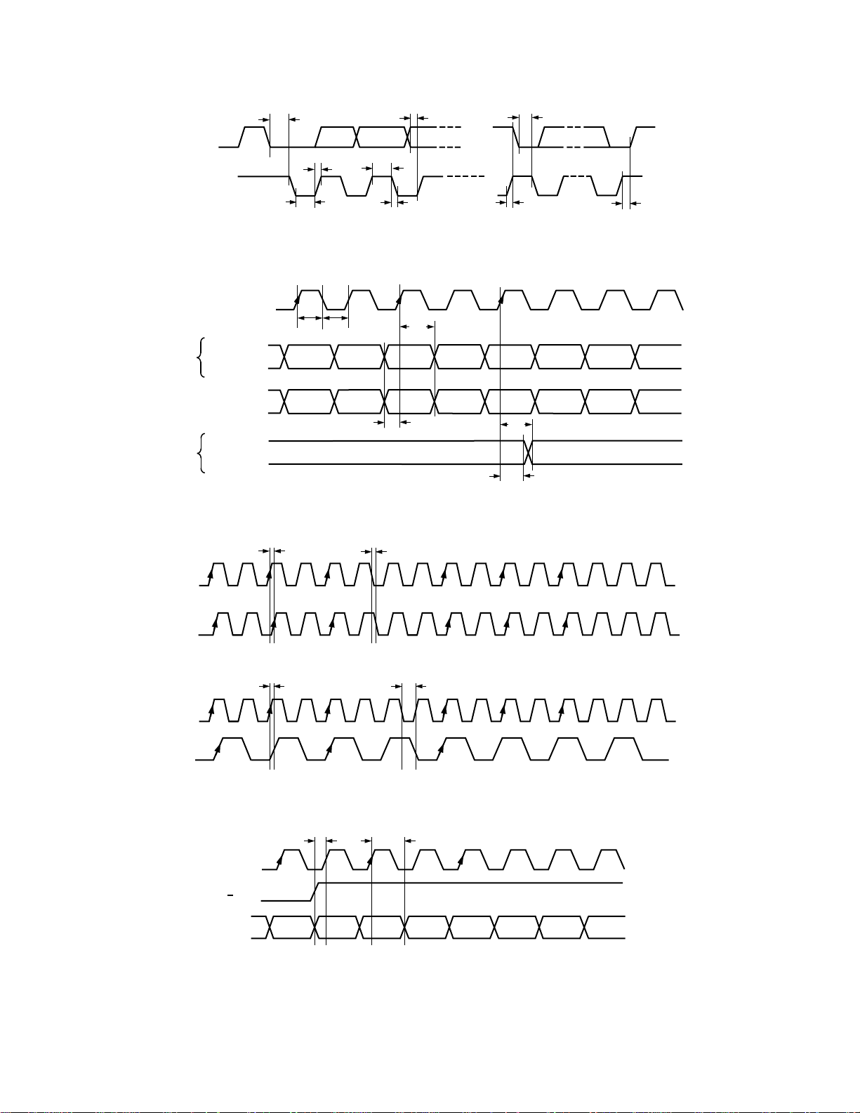
Figure 1. MPU Port Timing Diagram
t
t
9
10
t
12
t
3
t
4
t
8
CONTROL
O/PS
CLOCK
CLOCK/2
CLOCK
CLOCK/2
PIXEL INPUT
DATA
HSYNC,
FIELD/VSYNC,
BLANK
Cb Y Cr Y Cb Y
t
11
t
13
t
14
Figure 2. Pixel and Control Data Timing Diagram
t
16
t
16
t
17
t
17
Figure 3. Internal Timing Diagram
CLOCK
OSD
OSD0–2
EN
t
18
t
19
Figure 4. OSD Timing Diagram
–8–
REV. 0
ADV7177/ADV7178
WARNING!
ESD SENSITIVE DEVICE
ABSOLUTE MAXIMUM RATINGS
1
VAA to GND . . . . . . . . . . . . . . . . . . . . . . . . . . . . . . . . . . . 7 V
Voltage on Any Digital Input Pin . . GND – 0.5 V to V
Storage Temperature (T
Junction Temperature (T
Lead Temperature (Soldering, 10 sec) . . . . . . . . . . . . . +260°C
Analog Outputs to GND
NOTES
1
Stresses above those listed under Absolute Maximum Ratings may cause permanent
damage to the device. This is a stress rating only; functional operation of the device
at these or any other conditions above those listed in the operational sections of this
specification is not implied. Exposure to absolute maximum rating conditions for
extended periods may affect device reliability.
2
Analog output short circuit to any power supply or common can be of an indefinite
duration.
) . . . . . . . . . . . . . . –65°C to +150°C
S
) . . . . . . . . . . . . . . . . . . . . . . +150°C
J
2
␣ . . . . . . . . . . . . . . GND – 0.5 to V
+ 0.5 V
AA
AA
ORDERING GUIDE
Temperature Package Package
Model Range Description Option
ADV7178KS 0°C to +70°C Plastic Quad Flatpack S-44
ADV7177KS 0°C to +70°C Plastic Quad Flatpack S-44
PACKAGE THERMAL PERFORMANCE
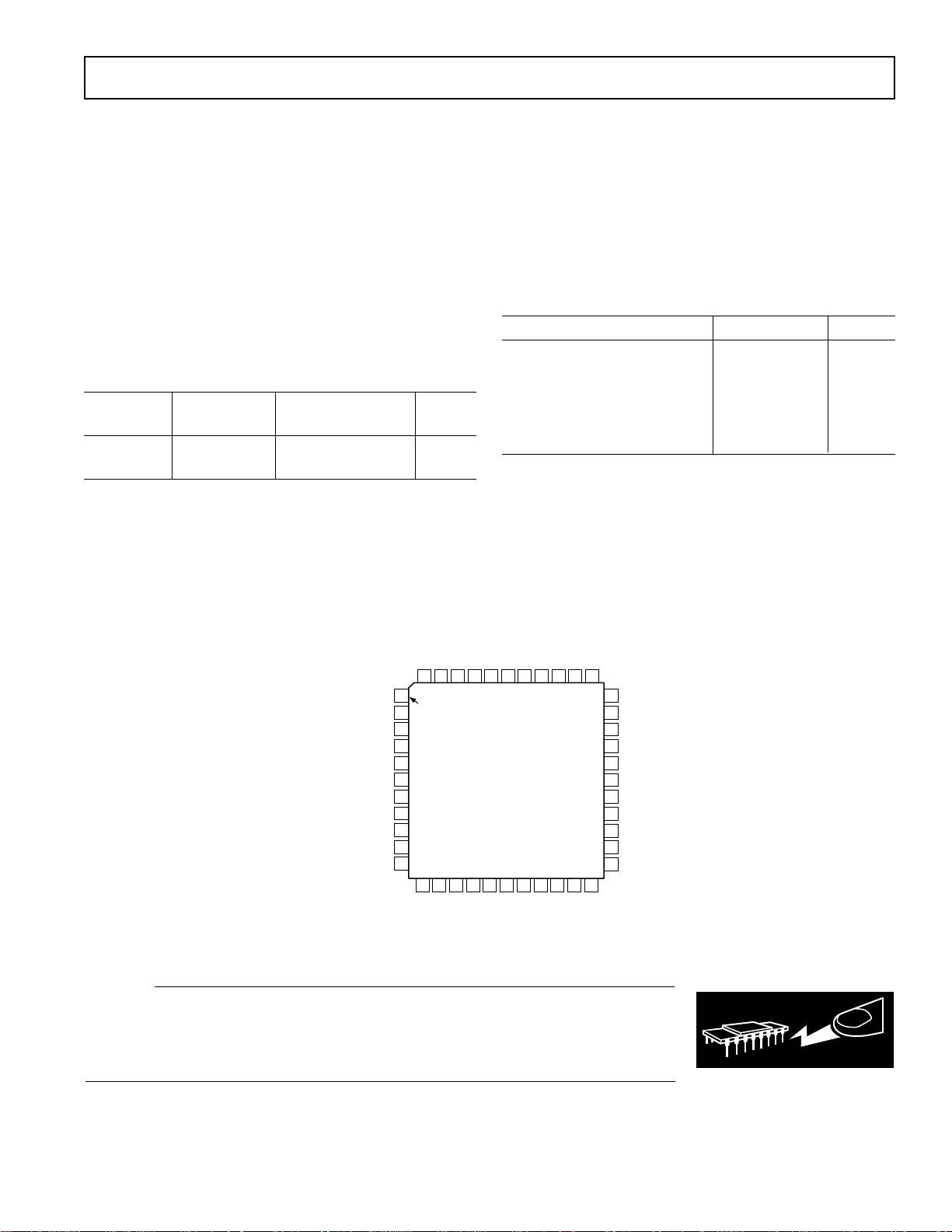
The 44-lead PQFP package used for this device has a junction-
to-ambient thermal resistance (θ
PCB of 53.2°C/W. The junction-to-case thermal resistance (θ
) in still air on a four-layer
JA
)
JC
is 18.8°C/W.
Care must be taken when operating the part in certain conditions to prevent overheating. Table I illustrates what conditions
are to be used when using the part.
Table I. Allowable Operating Conditions for ADV7177/
ADV7178 in 44-Lead PQFP Package
Condition 5 V 3 V
3 DACs ON, Double 75R
3 DACs ON, Low Power
3 DACs ON, Buffered
2
3
1
No Yes
Yes Yes
Yes Yes
2 DACs ON, Double 75R No Yes
2 DACs ON, Low Power Yes Yes
2 DACs ON, Buffered Yes Yes
NOTES
1
DAC ON, Double 75R refers to a condition where the DACs are terminated
into a double 75R load and low power mode is disabled.
2
DAC ON, Low Power refers to a condition where the DACs are terminated in a
double 75R load and low power mode is enabled.
3
DAC ON, Buffered refers to a condition where the DAC current is reduced to
5 mA and external buffers are used to drive the video loads.
PIN CONFIGURATION
P4
P2
P1
V
CLOCK/2
P10
P11
P12
OSD_EN
CLOCK
CLOCK
4344 36 35 3437
1
AA
PIN 1
IDENTIFIER
2
3
P5
4
P6
5
P7
6
P8
7
P9
8
9
10
11
12 13 14 15 16 17 18 192021 22
P14
P13
P3
GND
42
40 39 3841
ADV7177/ADV7178
PQFP
TOP VIEW
(Not to Scale)
P15
HSYNC
FIELD/VSYNC
BLANK
ALSB
P0
GND
OSD_2
AA
V
OSD_0
OSD_1
GND
RESET
33
32
31
30
29
28
27
26
25
24
23
R
SET
V
REF
DAC A
V
AA
GND
V
AA
DAC B
DAC C
COMP
SDATA
SCLOCK
CAUTION
ESD (electrostatic discharge) sensitive device. Electrostatic charges as high as 4000 V readily
accumulate on the human body and test equipment and can discharge without detection.
Although the ADV7177/ADV7178 feature proprietary ESD protection circuitry, permanent
damage may occur on devices subjected to high energy electrostatic discharges. Therefore, proper
ESD precautions are recommended to avoid performance degradation or loss of functionality.
–9–REV. 0

ADV7177/ADV7178
PIN FUNCTION DESCRIPTIONS
Pin Input/
No. Mnemonic Output Function
1, 20, 28, 30 V
AA
P +5 V Supply.
2 CLOCK/2 O Synchronous Clock output signal. Can be either 27 MHz or 13.5 MHz; this
can be controlled by MR32 and MR33 in Mode Register 3.
3–10, 12–14, P15–P0 I 8-Bit 4:2:2 Multiplexed YCrCb Pixel Port (P7–P0) or 16-Bit YCrCb
37–41 Pixel Port (P15–P0). P0 represents the LSB.
11 OSD_EN I Enables OSD input data on the video outputs.
15 HSYNC I/O HSYNC (Modes 1 and 2) Control Signal. This pin may be configured to
output (Master Mode) or accept (Slave Mode) Sync signals.
16 FIELD/VSYNC I/O Dual Function FIELD (Mode 1) and
VSYNC (Mode 2) Control Signal. This
pin may be configured to output (Master Mode) or accept (Slave Mode)
these control signals.
17 BLANK I/O Video Blanking Control Signal. The pixel inputs are ignored when this is
Logic Level “0.” This signal is optional.
18 ALSB I TTL Address Input. This signal sets up the LSB of the MPU address.
19, 21, 29, 42 GND G Ground Pin.
22 RESET I The input resets the on-chip timing generator and sets the ADV7177/ADV7178
into default mode. This is NTSC operation, Timing Slave Mode 0, 8-Bit
Operation, 2 × Composite and S VHS out.
23 SCLOCK I MPU Port Serial Interface Clock Input.
24 SDATA I/O MPU Port Serial Data Input/Output.
25 COMP O Compensation Pin. Connect a 0.1 µF Capacitor from COMP to V
AA
.
26 DAC C O DAC C Analog Output.
27 DAC B O DAC B Analog Output.
31 DAC A O DAC A Analog Output.
32 V
33 R
REF
SET
I/O Voltage Reference Input for DACs or Voltage Reference Output (1.2 V).
I A 300 Ω resistor connected from this pin to GND is used to control full-scale
amplitudes of the Video Signals.
34–36 OSD_0–2 I On Screen Display Inputs.
43 CLOCK O Crystal Oscillator output (to crystal). Leave unconnected if no crystal is used.
44 CLOCK I Crystal Oscillator input. If no crystal is used this pin can be driven by an
external TTL Clock source; it requires a stable 27 MHz reference Clock for
standard operation. Alternatively, a 24.52 MHz (NTSC) or 29.5 MHz (PAL)
can be used for square pixel operation.
–10–
REV. 0
ADV7177/ADV7178
(Continued from page 1)
compatible with worldwide standards. The 4:2:2 YUV video
data is interpolated to two times the pixel rate. The colordifference components (UV) are quadrature modulated using
a subcarrier frequency generated by an on-chip 32-bit digital
synthesizer (also running at two times the pixel rate). The two
times pixel rate sampling allows for better signal-to-noise ratio.
A 32-bit DDS with a 9-bit look-up table produces a superior
subcarrier in terms of both frequency and phase. In addition
to the composite output signal, there is the facility to output
S-Video (Y/C) video, YUV or RGB video.
Each analog output is capable of driving the full video-level
(34.7 mA) signal into an unbuffered, doubly terminated 75 Ω
load. With external buffering, the user has the additional option
to scale back the DAC output current to 5 mA min, thereby significantly reducing the power dissipation of the device.
The ADV7177/ADV7178 also supports both PAL and NTSC
square pixel operation.
The output video frames are synchronized with the incoming
data timing reference codes. Optionally, the encoder accepts
(and can generate) HSYNC, VSYNC and FIELD timing signals.
These timing signals can be adjusted to change pulsewidth and
position while the part is in the master mode. The encoder
requires a single two times pixel rate (27 MHz) clock for standard
operation. Alternatively, the encoder requires a 24.54 MHz clock
for NTSC or 29.5 MHz clock for PAL square pixel mode
operation. All internal timing is generated on-chip.
The ADV7177/ADV7178 modes are set up over a two-wire
serial bidirectional port (I
2
C-Compatible) with two slave addresses.
Functionally the ADV7178 and ADV7177 are the same with
the exception that the ADV7178 can output the Macrovision
anticopy algorithm, and OSD is only supported on the ADV7177.
The ADV7177/ADV7178 is packaged in a 44-lead thermally
enhanced PQFP package.
DATA PATH DESCRIPTION
For PAL B, D, G, H, I, M, N and NTSC M, N modes, YCrCb
4:2:2 data is input via the CCIR-656 compatible pixel port at a
27 MHz data rate. The pixel data is demultiplexed to from
three data paths. Y typically has a range of 16 to 235, Cr and
Cb typically have a range of 128 ± 112; however, it is possible
to input data from 1 to 254 on both Y, Cb and Cr. The
ADV7177/ADV7178 supports PAL (B, D, G, H, I, N, M) and
NTSC (with and without Pedestal) standards. The appropriate SYNC, BLANK and Burst levels are added to the YCrCb
data. Macrovision antitaping (ADV7178 only), closed captioning,
OSD (ADV7177 only), and teletext levels are also added to Y,
and the resultant data is interpolated to a rate of 27 MHz. The
interpolated data is filtered and scaled by three digital FIR
filters.
The U and V signals are modulated by the appropriate subcarrier
sine/cosine phases and added together to make up the chrominance signal. The luma (Y) signal can be delayed 1–3 luma
cycles (each cycle is 74 ns) with respect to the chroma signal.
The luma and chroma signals are then added together to make
up the composite video signal. All edges are slew rate limited.
The YCrCb data is also used to generate RGB data with
appropriate SYNC and BLANK levels. The RGB data is in
synchronization with the composite video output. Alternatively
analog YUV data can be generated instead of RGB.
The three 9-bit DACs can be used to output:
1. RGB Video.
2. YUV Video
3. One Composite Video Signal + LUMA and CHROMA
3. (S-Video).
Alternatively, each DAC can be individually powered off if not
required.
Video output levels are illustrated in Appendix 3, Appendix 4 and
Appendix 5.
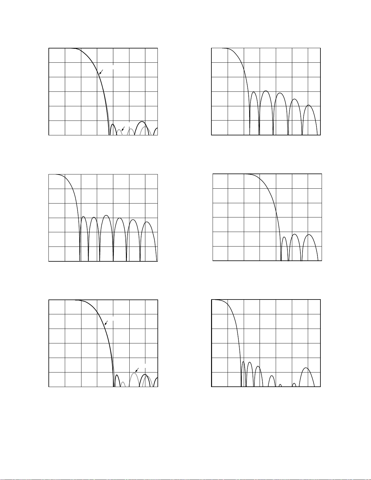
INTERNAL FILTER RESPONSE
The Y filter supports several different frequency responses,
including two 4.5 MHz/5.0 MHz low-pass responses, PAL/
NTSC subcarrier notch responses and a PAL/NTSC extended
response. The U and V filters have a 2/2.4 MHz low-pass
response for NTSC/PAL. These filter characteristics are illustrated in Figures 7 to 13.
PASSBAND
FILTER SELECTION
MR04 MR03
NTSC 0 0 2.3 0.026 7.0
PAL 0 0 3.4 0.098 7.3
NTSC 0 1 1.0 0.085 3.57
PAL 0 1 1.4 0.107 4.43
NTSC/PAL 1 0 4.0 0.150 7.5
NTSC 1 1 2.3 0.054 7.0
PAL 1 1 3.4 0.106 7.3
CUTOFF (MHz)
PASSBAND
RIPPLE (dB)
STOPBAND
CUTOFF (MHz)
Figure 5. Luminance Internal Filter Specifications
PASSBAND
FILTER SELECTION
NTSC 1.0 0.085 3.2
PAL 1.3 0.04 4.0
CUTOFF (MHz)
PASSBAND
RIPPLE (dB)
STOPBAND
CUTOFF (MHz)
STOPBAND
ATTENUATION (dB)
Figure 6. Chrominance Internal Filter Specifications
–11–REV. 0
STOPBAND
ATTENUATION (dB)
>
54 4.2
>
50 5.0
>
27.6 2.1
>
29.3 2.7
>
40 5.35
>
54 4.2
>
50.3 5.0
ATTENUATION @
>
40 0.3 2.05
>
40 0.02 2.45
F
3 dB
1.3MHz (dB)
F
3 dB
ADV7177/ADV7178
0
–10
–20
–30
AMPLITUDE – dB
–40
–50
–60
0 246
FREQUENCY – MHz
Figure 7. NTSC Low-Pass Filter
0
–10
–20
–30
TYPE A
TYPE B
81210
0
–10
–20
–30
AMPLITUDE – dB
–40
–50
–60
0 2468 1210
FREQUENCY – MHz
Figure 10. PAL Notch Filter
0
–10
–20
–30
AMPLITUDE – dB
–40
–50
–60
0 2468 1210
FREQUENCY – MHz
Figure 8. NTSC Notch Filter
0
–10
–20
–30
AMPLITUDE – dB
–40
–50
–60
0 2468 1210
TYPE A
FREQUENCY – MHz
Figure 9. PAL Low-Pass Filter
TYPE B
AMPLITUDE – dB
–40
–50
–60
0 2468 1210
FREQUENCY – MHz
Figure 11. NTSC/PAL Extended Mode Filter
0
–10
–20
–30
AMPLITUDE – dB
–40
–50
–60
0 2468 1210
FREQUENCY – MHz
Figure 12. NTSC UV Filter
–12–
REV. 0
 Loading...