High Quality, 10-Bit, Digital CCIR-601
a
FEATURES
ITU-R BT601/656 YCrCb to PAL/NTSC Video Encoder
High Quality 10-Bit Video DACs
Integral Nonlinearity <1 LSB at 10 Bits
NTSC-M, PAL-M/N, PAL-B/D/G/H/I
Single 27 MHz Clock Required (32 Oversampling)
80 dB Video SNR
32-Bit Direct Digital Synthesizer for Color Subcarrier
Multistandard Video Output Support:
Composite (CVBS)
Component S-Video (Y/C)
Component YUV and RGB
EuroSCART Output (RGB + CVBS/LUMA)
Video Input Data Port Supports:
CCIR-656 4:2:2 8-Bit Parallel Input Format
4:2:2 16-Bit Parallel Input Format
SMPTE 170M NTSC Compatible Composite Video
ITU-R BT.470 PAL Compatible Composite Video
Full Video Output Drive or Low Signal Drive Capability
34.7 mA max into 37.5 V (Doubly-Terminated 75R)
5 mA min with External Buffers
Programmable Simultaneous Composite
and S-Video Y/C or RGB (SCART)/YUV Video Outputs
Programmable Luma Filters (Low-Pass/Notch/Extended)
Programmable VBI (Vertical Blanking Interval)
Programmable Subcarrier Frequency and Phase
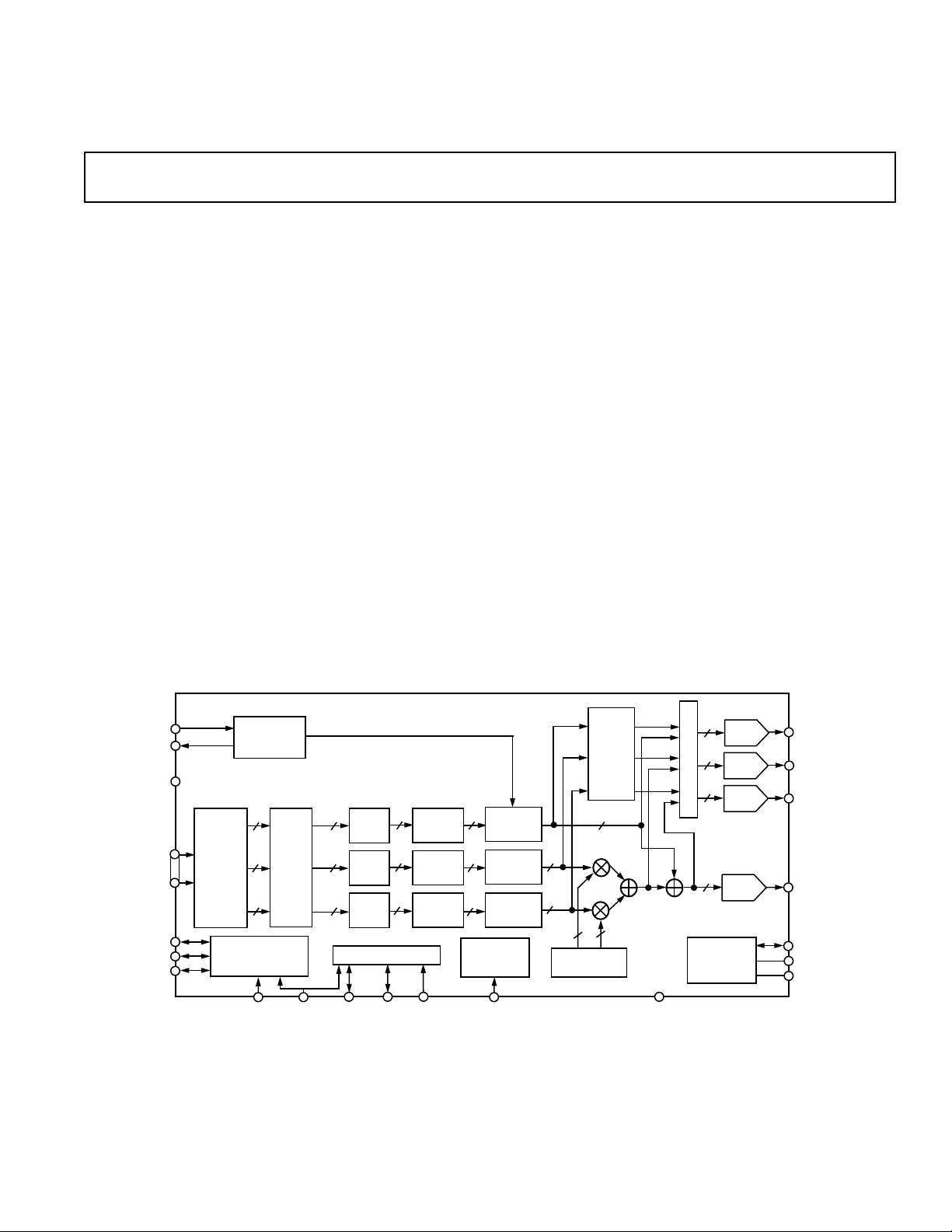
FUNCTIONAL BLOCK DIAGRAM
to PAL/NTSC Video Encoder
ADV7175A/ADV7176A*
Programmable LUMA Delay
Individual ON/OFF Control of Each DAC
CCIR and Square Pixel Operation
Integrated Subcarrier Locking to External Video Source
Color Signal Control/Burst Signal Control
Interlaced/Noninterlaced Operation
Complete On-Chip Video Timing Generator
Programmable Multimode Master/Slave Operation
Macrovision Antitaping Rev 7.01 (ADV7175A Only)**
Closed Captioning Support
Teletext Insertion Port (PAL-WST)
Onboard Color Bar Generation
Onboard Voltage Reference
2-Wire Serial MPU Interface (I
Single Supply +5 V or + 3 V Operation
Small 44-Lead PQFP Thermally Enhanced Package
APPLICATIONS
MPEG-1 and MPEG-2 Video, DVD, Digital Satellite/
Cable Systems (Set Top Boxes/IRDs), Digital TVs,
CD Video/Karaoke, Video Games, PC Video/Multimedia
GENERAL DESCRIPTION
The ADV7175A/ADV7176A is an integrated digital video encoder that converts Digital CCIR-601 4:2:2 8 or 16-bit component video data into a standard analog baseband television
2
C Compatible)
(Continued on page 11)
M
U
TTX
TTXREQ
V
AA
COLOR
DATA
P7–P0
P15–P8
HSYNC
FIELD/VSYNC
BLANK
4:2:2 TO
4:4:4
INTER-
POLATOR
VIDEO TIMING
GENERATOR
TELETEXT
INSERTION
BLOCK
8
YCrCb
8
MATRIX
8
CLOCK
8
TO
YUV
SCLOCK SDATA ALSB
RESET
ADD
SYNC
ADD
BURST
ADD
BURST
2
I
C MPU PORT
8
88
88
INTER-
POLATOR
INTER-
POLATOR
INTER-
POLATOR
Y
8
LOW-PASS
FILTER
U
8
LOW-PASS
FILTER
V
8
LOW-PASS
FILTER
REAL-TIME
CONTROL
CIRCUIT
SCRESET/RTC
10
10
10
DDS BLOCK
YUV TO
MATRIX
10
SIN/COS
RBG
ADV7175A/ADV7176A
10
GND
10
L
T
I
10
P
L
E
10
X
E
R
10
VOLTAGE
REFERENCE
CIRCUIT
10-BIT
DAC
10-BIT
DAC
10-BIT
DAC
10-BIT
DAC
DAC D (PIN 27)
DAC C (PIN 26)
DAC B (PIN 31)
DAC A (PIN 32)
V
REF
R
SET
COMP
*Protected by U.S. patents numbers 5,343,196 and 5,442,355 and other intellectual property rights.
**This device is protected by U.S. Patent Numbers 4631603, 4577216, 4819098 and other intellectual property rights. The Macrovision anticopy process is
licensed for noncommercial home use only, which is its sole intended use in the device. Please contact sales office for latest Macrovision version available.
NOTE: ITU-R and CCIR are used interchangeably in this document (ITU-R has replaced CCIR recommendations).
REV. B
Information furnished by Analog Devices is believed to be accurate and
reliable. However, no responsibility is assumed by Analog Devices for its
use, nor for any infringements of patents or other rights of third parties
which may result from its use. No license is granted by implication or
otherwise under any patent or patent rights of Analog Devices.
One Technology Way, P.O. Box 9106, Norwood, MA 02062-9106, U.S.A.
Tel: 781/329-4700 World Wide Web Site: http://www.analog.com
Fax: 781/326-8703 © Analog Devices, Inc., 1998

ADV7175A/ADV7176A–SPECIFICA TIONS
5 V SPECIFICATIONS
(VAA = +5 V 6 5%1, V
Parameter Conditions
= 1.235 V R
REF
1
= 150 V. All specifications T
SET
Min Typ Max Units
MIN
STATIC PERFORMANCE
Resolution (Each DAC) 10 Bits
Accuracy (Each DAC)
Integral Nonlinearity ±1 LSB
Differential Nonlinearity Guaranteed Monotonic ±1 LSB
DIGITAL INPUTS
Input High Voltage, V
Input Low Voltage, V
Input Current, I
Input Current, I
Input Capacitance, C
INL
3
IN
4
IN
IN
INH
VIN = 0.4 V or 2.4 V ±1 µA
VIN = 0.4 V or 2.4 V ±50 µA
2V
DIGITAL OUTPUTS
Output High Voltage, V
Output Low Voltage, V
OL
OH
I
I
= 400 µA 2.4 V
SOURCE
= 3.2 mA 0.4 V
SINK
Three-State Leakage Current 10 µA
Three-State Output Capacitance 10 pF
2
to T
unless otherwise noted)
MAX
0.8 V
10 pF
ANALOG OUTPUTS
Output Current
Output Current
5
6
33 34.7 37 mA
5mA
DAC-to-DAC Matching 0.6 5 %
Output Compliance, V
Output Impedance, R
OUT
Output Capacitance, C
OC
OUT
I
= 0 mA 30 pF
OUT
0 +1.4 V
15 kΩ
VOLTAGE REFERENCE
Reference Range, V
POWER REQUIREMENTS
V
AA
Normal Power Mode
I
(max)
DAC
I
(min)
DAC
9
I
CCT
Low Power Mode
I
(max)
DAC
I
(min)
DAC
9
I
CCT
REF
7
8
8
8
8
I
VREFOUT
= 20 µA 1.112 1.235 1.359 V
4.75 5.0 5.25 V
150 155 mA
20 mA
100 150 mA
80 mA
15 mA
100 150 mA
Power Supply Rejection Ratio COMP = 0.1 µF 0.01 0.5 %/%
NOTES
1
The max/min specifications are guaranteed over this range. The max/min values are typical over 4.75 V to 5.25 V.
2
Temperature range T
3
All digital input pins except pins RESET and RTC/SCRESET.
4
Excluding all digital input pins except pins RESET and RTC/SCRESET.
5
Full drive into 37.5 Ω load.
6
Minimum drive current (used with buffered/scaled output load).
7
Power measurements are taken with Clock Frequency = 27 MHz. Max TJ = 110°C.
8
I
is the total current (min corresponds to 5 mA output per DAC, max corresponds to 37 mA output per DAC) to drive all four DACs. Turning off individual
DAC
DACs reduces I
9
I
(Circuit Current) is the continuous current required to drive the device.
CCT
Specifications subject to change without notice.
to T
MIN
correspondingly.
DAC
: 0°C to 70°C.
MAX
–2–
REV. B

ADV7175A/ADV7176A
3.3 V SPECIFICATIONS
(VAA = +3.0 V – 3.6 V1, V
Parameter Conditions
STATIC PERFORMANCE
3
= 1.235 V R
REF
1
= 300 V. All specifications T
SET
Min Typ Max Units
MIN
Resolution (Each DAC) 10 Bits
Accuracy (Each DAC)
Integral Nonlinearity ±1 LSB
Differential Nonlinearity Guaranteed Monotonic ±1 LSB
DIGITAL INPUTS
Input High Voltage, V
Input Low Voltage, V
Input Current, I
Input Current, I
Input Capacitance, C
IN
IN3,
3, 4
INH
INL
5
IN
VIN = 0.4 V or 2.4 V ±1 µA
VIN = 0.4 V or 2.4 V ±50 µA
DIGITAL OUTPUTS
Output High Voltage, V
Output Low Voltage, V
OH
OL
Three-State Leakage Current
Three-State Output Capacitance
ANALOG OUTPUTS
Output Current
Output Current
3
6, 7
8
3
3
I
I
= 400 µA 2.4 V
SOURCE
= 3.2 mA 0.4 V
SINK
16.5 17.35 18.5 mA
DAC-to-DAC Matching 2.0 %
Output Compliance, V
Output Impedance, R
Output Capacitance, C
POWER REQUIREMENTS
V
AA
Normal Power Mode
I
DAC
I
DAC
I
CCT
Low Power Mode
I
DAC
I
DAC
I
CCT
(max)
(min)
9
(max)
(min)
11
10
10
10
10
OC
OUT
OUT
3, 9
I
= 0 mA 30 pF
OUT
0 +1.4 V
3.0 3.3 3.6 V
Power Supply Rejection Ratio COMP = 0.1 µF 0.01 0.5 %/%
NOTES
11
The max/min specifications are guaranteed over this range. The max/min values are typical over 3.0 V to 3.6 V.
12
Temperature range T
13
Guaranteed by characterization.
14
All digital input pins except pins RESET and RTC/SCRESET.
15
Excluding all digital input pins except pins RESET and RTC/SCRESET.
16
Full drive into 37.5 Ω load.
17
DACs can output 35 mA typically at 3.3 V (R
18
Minimum drive current (used with buffered/scaled output load).
19
Power measurements are taken with Clock Frequency = 27 MHz. Max TJ = 110°C.
10
I
is the total current (min corresponds to 5 mA output per DAC, max corresponds to 38 mA output per DAC) to drive all four DACs. Turning off individual
DAC
DACs reduces I
11
I
(Circuit Current) is the continuous current required to drive the device.
CCT
Specifications subject to change without notice.
to T
MIN
correspondingly.
DAC
: 0°C to 70°C.
MAX
= 150 Ω and RL = 75 Ω), optimum performance obtained at 18 mA DAC current (R
SET
2
to T
unless otherwise noted)
MAX
2V
0.8 V
10 pF
10 µA
10 pF
5mA
15 kΩ
150 155 mA
20 mA
45 mA
75 mA
15 mA
45 mA
= 300 Ω and RL = 150 Ω.
SET
–3–REV. B

ADV7175A/ADV7176A–SPECIFICA TIONS
(VAA = +4.75 V – 5.25 V1, V
5 V DYNAMIC SPECIFICATIONS
Parameter Conditions
1
unless otherwise noted.)
1
Filter Characteristics
Luma Bandwidth3 (Low-Pass Filter) NTSC Mode
Stopband Cutoff >54 dB Attenuation 7.0 MHz
Passband Cutoff F
3 dB
>3 dB Attenuation 4.2 MHz
Chroma Bandwidth NTSC Mode
Stopband Cutoff >40 dB Attenuation 3.2 MHz
Passband Cutoff F
Luma Bandwidth
3 dB
3
(Low-Pass Filter) PAL MODE
>3 dB Attenuation 2.0 MHz
Stopband Cutoff >50 dB Attenuation 7.4 MHz
Passband Cutoff F
3 dB
>3 dB Attenuation 5.0 MHz
Chroma Bandwidth PAL MODE
Stopband Cutoff >40 dB Attenuation 4.0 MHz
Passband Cutoff F
Differential Gain
Differential Phase
Differential Gain
Differential Phase
4
SNR
(Pedestal) RMS 80 dB rms
4
SNR
(Pedestal) Peak Periodic 70 dB p-p
4
SNR
(Ramp) RMS 60 dB rms
4
SNR
(Ramp) Peak Periodic 58 dB p-p
Hue Accuracy
Color Saturation Accuracy
Chroma Nonlinear Gain
Chroma Nonlinear Phase
Chroma Nonlinear Phase
Chroma/Luma Intermod
Chroma/Luma Intermod
Chroma/Luma Gain Ineq
Chroma/Luma Delay Ineq
Luminance Nonlinearity
Chroma AM Noise
Chroma PM Noise
NOTES
1
The max/min specifications are guaranteed over this range. The max/min values are typical over 4.75 V to 5.25 V.
2
Temperature range T
3
These specifications are for the low-pass filter only and guaranteed by design. For other internal filters, see Figure 4.
4
Guaranteed by characterization.
Specifications subject to change without notice.
3 dB
4
4
4
4
4
4
4
4
4
4
4
4
4
4
4
4
to T
MIN
: 0°C to +70°C.
MAX
>3 dB Attenuation 2.4 MHz
Normal Power Mode 0.4 %
Normal Power Mode 0.4 Degree
Lower Power Mode 2.0 %
Lower Power Mode 1.0 Degree
Referenced to 40 IRE 0.6 ±%
NTSC 0.2 ±Degree
PAL 0.4 ±Degree
Referenced to 714 mV (NTSC) 0.1 ±%
Referenced to 700 mV (PAL) 0.1 ±%
= 1.235 V R
REF
= 150 V. All specifications T
SET
MIN
to T
Min Typ Max Units
0.5 Degree
1.0 %
0.6 ±%
2.0 ns
1.0 ± %
66 dB
63 dB
MAX
2
–4–
REV. B

ADV7175A/ADV7176A
(VAA = +3.0 V – 3.6 V1, V
1
3.3 V DYNAMIC SPECIFICATIONS
Parameter Conditions
unless otherwise noted.)
1
Filter Characteristics
Luma Bandwidth3 (Low-Pass Filter) NTSC Mode
Stopband Cutoff >54 dB Attenuation 7.0 MHz
Passband Cutoff F
3 dB
>3 dB Attenuation 4.2 MHz
Chroma Bandwidth NTSC Mode
Stopband Cutoff >40 dB Attenuation 3.2 MHz
Passband Cutoff F
Luma Bandwidth
3 dB
3
(Low-Pass Filter) PAL MODE
>3 dB Attenuation 2.0 MHz
Stopband Cutoff >50 dB Attenuation 7.4 MHz
Passband Cutoff F
3 dB
>3 dB Attenuation 5.0 MHz
Chroma Bandwidth PAL MODE
Stopband Cutoff >40 dB Attenuation 4.0 MHz
Passband Cutoff F
Differential Gain
Differential Phase
4
SNR
(Pedestal) RMS 75 dB rms
4
SNR
(Pedestal) Peak Periodic 68 dB p-p
4
SNR
(Ramp) RMS 58 dB rms
4
SNR
(Ramp) Peak Periodic 56 dB p-p
Hue Accuracy
Color Saturation Accuracy
Luminance Nonlinearity
Chroma AM Noise
Chroma PM Noise
Chroma AM Noise
Chroma PM Noise
NOTES
1
The max/min specifications are guaranteed over this range. The max/min values are typical over 3.0 V to 3.6 V.
2
Temperature range T
3
These specifications are for the low-pass filter only and guaranteed by design. For other internal filters, see Figure 4.
4
Guaranteed by characterization.
Specifications subject to change without notice.
3 dB
4
4
4
4
4
4
4
4
4
to T
MIN
: 0°C to +70°C.
MAX
>3 dB Attenuation 2.4 MHz
Normal Power Mode 0.7 %
Normal Power Mode 0.5 Degree
NTSC 67 dB
NTSC 63 dB
PAL 64 dB
PAL 63 dB
= 1.235 V R
REF
= 300 V. All specifications T
SET
MIN
to T
Min Typ Max Units
1.0 Degree
1.2 %
1.1 ±%
MAX
2
–5–REV. B

ADV7175A/ADV7176A
to T
MAX
2
unless
5 V TIMING SPECIFICATIONS
(VAA = 4.75 V – 5.25 V1, V
otherwise noted.)
= 1.235 V R
REF
= 150 V. All specifications T
SET
MIN
Parameter Conditions Min Typ Max Units
MPU PORT
3, 4
SCLOCK Frequency 0 100 kHz
SCLOCK High Pulsewidth, t
SCLOCK Low Pulsewidth, t
Hold Time (Start Condition), t
Setup Time (Start Condition), t
Data Setup Time, t
5
SDATA, SCLOCK Rise Time, t
SDATA, SCLOCK Fall Time, t
Setup Time (Stop Condition), t
ANALOG OUTPUTS
3, 5
1
2
After This Period the First Clock Is Generated 4.0 µs
3
Relevant for Repeated Start Condition 4.7 µs
4
6
7
8
4.0 µs
4.7 µs
250 ns
1 µs
300 ns
4.7 µs
Analog Output Delay 5ns
DAC Analog Output Skew 0 ns
CLOCK CONTROL
AND PIXEL PORT
F
CLOCK
Clock High Time, t
Clock Low Time, t
Data Setup Time, t
Data Hold Time, t
Control Setup Time, t
Control Hold Time, t
Digital Output Access Time, t
Digital Output Hold Time, t
Pipeline Delay, t
TELETEXT PORT
Digital Output Access Time, t
Data Setup Time, t
Data Hold Time, t
RESET CONTROL
3, 6
27 MHz
9
10
11
12
11
12
13
14
15
3, 7
16
17
18
3, 4
8ns
8ns
3.5 ns
4ns
4ns
3ns
24 ns
4ns
37 Clock Cycles
20 ns
1ns
2ns
RESET Low Time 6 ns
NOTES
1
The max/min specifications are guaranteed over this range.
2
Temperature range T
3
TTL input values are 0 to 3 volts, with input rise/fall times ≤ 3 ns, measured between the 10% and 90% points. Timing reference points at 50% for inputs and
outputs. Analog output load ≤ 10 pF.
4
Guaranteed by characterization.
5
Output delay measured from the 50% point of the rising edge of CLOCK to the 50% point of full-scale transition.
6
Pixel Port consists of the following:
Pixel Inputs: P15–P0
Pixel Controls: HSYNC, FIELD/VSYNC, BLANK
Clock Input: CLOCK
7
Teletext Port consists of the following:
Teletext Output: TTXREQ
Teletext Input: TTX
Specifications subject to change without notice.
MIN
to T
: 0oC to +70oC.
MAX
–6–
REV. B

ADV7175A/ADV7176A
2
to T
unless
MAX
1 µs
300 ns
3.3 V TIMING SPECIFICATIONS
(VAA = 3.0 – 3.61, V
otherwise noted.)
= 1.235 V R
REF
= 300 V. All specifications T
SET
MIN
Parameter Conditions Min Typ Max Units
MPU PORT
3, 4
SCLOCK Frequency 0 100 kHz
SCLOCK High Pulsewidth, t
SCLOCK Low Pulsewidth, t
Hold Time (Start Condition), t
Setup Time (Start Condition), t
Data Setup Time, t
5
SDATA, SCLOCK Rise Time, t
SDATA, SCLOCK Fall Time, t
Setup Time (Stop Condition), t
ANALOG OUTPUTS
3, 5
1
2
After This Period the First Clock Is Generated 4.0 µs
3
for Repeated Start Condition 4.7 µs
4
6
7
8
4.0 µs
4.7 µs
250 ns
4.7 µs
Analog Output Delay 7ns
DAC Analog Output Skew 0 ns
CLOCK CONTROL
AND PIXEL PORT
F
CLOCK
Clock High Time, t
Clock Low Time, t
Data Setup Time, t
Data Hold Time, t
Control Setup Time, t
Control Hold Time, t
Digital Output Access Time, t
Digital Output Hold Time, t
Pipeline Delay, t
TELETEXT PORT
Digital Output Access Time t
Data Setup Time, t
Data Hold Time, t
RESET CONTROL
3, 4, 6, 7
10
12
15
3, 6, 8
18
3, 4
27 MHz
9
8ns
8ns
11
3.5 ns
4ns
11
12
13
14
4ns
3ns
24 ns
4ns
37 Clock Cycles
16
17
23 ns
2ns
2ns
RESET Low Time 6 ns
NOTES
1
The max/min specifications are guaranteed over this range.
2
Temperature range T
3
TTL input values are 0 to 3 volts, with input rise/fall times ≤ 3 ns, measured between the 10% and 90% points. Timing reference points at 50% for inputs and
outputs. Analog output load ≤ 10 pF.
4
Guaranteed by characterization.
5
Output delay measured from the 50% point of the rising edge of CLOCK to the 50% point of full-scale transition.
6
Characterized by design.
7
Pixel Port consists of the following:
Pixel Inputs: P15–P0
Pixel Controls: HSYNC, FIELD/VSYNC, BLANK
Clock Input: CLOCK
8
Teletext Port consists of the following:
Teletext Output: TTXREQ
Teletext Input: TTX
Specifications subject to change without notice.
MIN
to T
: 0oC to +70oC.
MAX
–7–REV. B
ADV7175A/ADV7176A
SDATA
SCLOCK
CONTROL
I/PS
FIELD/VSYNC,
CLOCK
HSYNC,
BLANK
t
t
3
t
6
t
2
5
t
1
t
7
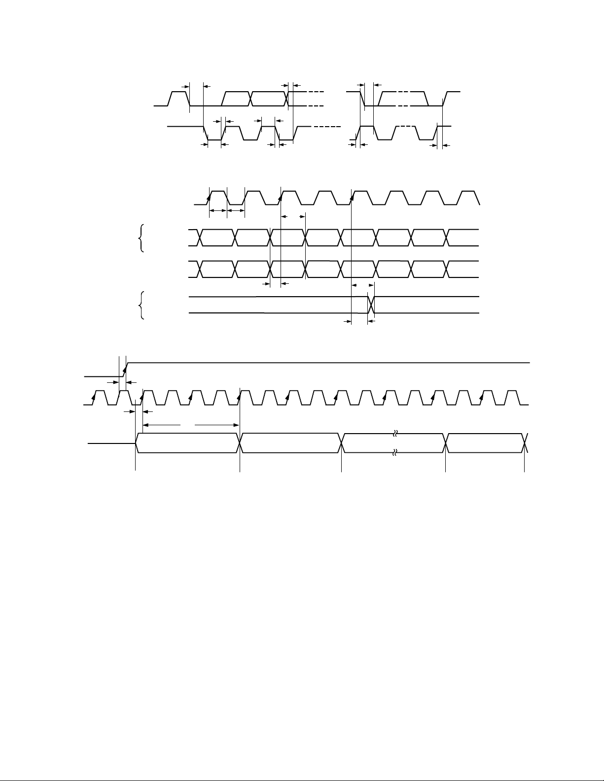
Figure 1. MPU Port Timing Diagram
t
t
9
10
t
12
t
3
t
4
t
8
TXTREQ
CLOCK
TXT
t
16
CONTROL
O/PS
t
17
PIXEL INPUT
DATA
HSYNC,
FIELD/VSYNC,
BLANK
4 CLOCK
CYCLES
Cb Y Cr Y Cb Y
t
11
t
13
t
14
Figure 2. Pixel and Control Data Timing Diagram
t
18
4 CLOCK
CYCLES
4 CLOCK
CYCLES
Figure 3. Teletext Timing Diagram
3 CLOCK
CYCLES
–8–
REV. B
ADV7175A/ADV7176A
WARNING!
ESD SENSITIVE DEVICE
ABSOLUTE MAXIMUM RATINGS
1
VAA to GND . . . . . . . . . . . . . . . . . . . . . . . . . . . . . . . . . . . 7 V
Voltage on Any Digital Input Pin . GND – 0.5 V to V
Storage Temperature (T
Junction Temperature (T
Lead Temperature (Soldering, 10 secs) . . . . . . . . . . . +260°C
Analog Outputs to GND
NOTES
1
Stresses above those listed under Absolute Maximum Ratings may cause permanent
damage to the device. This is a stress rating only; functional operation of the device
at these or any other conditions above those listed in the operational sections of this
specification is not implied. Exposure to absolute maximum rating conditions for
extended periods may affect device reliability.
2
Analog output short circuit to any power supply or common can be of an indefinite
duration.
) . . . . . . . . . . . . . . –65°C to +150°C
S
) . . . . . . . . . . . . . . . . . . . . . +150°C
J
2
. . . . . . . . . . . . . GND – 0.5 to V
+ 0.5 V
AA
AA
ORDERING GUIDE
Temperature Package Package
Model Range Description Option
ADV7175AKS 0°C to +70°C Plastic Quad Flatpack S-44
ADV7176AKS 0°C to +70°C Plastic Quad Flatpack S-44
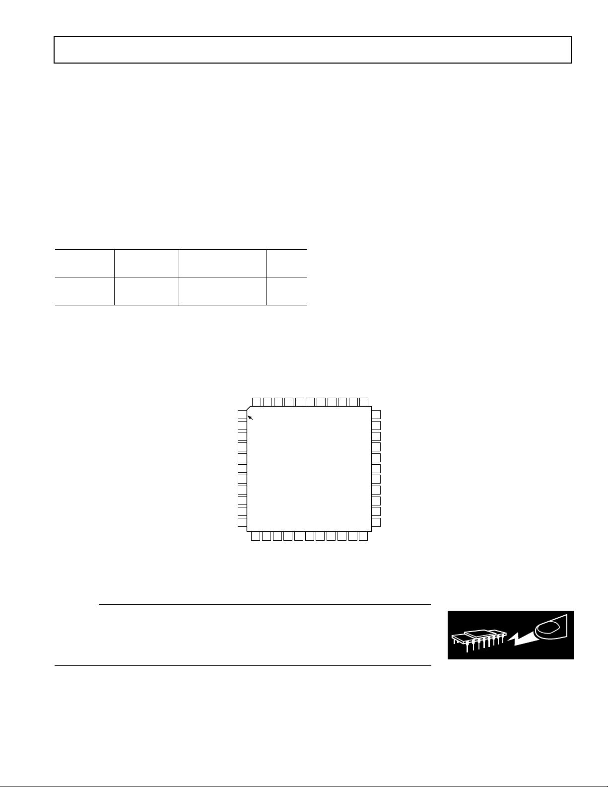
PIN CONFIGURATION
PACKAGE THERMAL PERFORMANCE
The 44-PQFP package used for this device takes advantage of
an ADI patented thermal coastline lead frame construction.
This maximizes heat transfer into the leads and reduces the
package thermal resistance.
The junction-to-ambient (θ
) thermal resistance in still air on a
JA
four-layer PCB is 35.5°C/W. The junction-to-case thermal
resistance (θ
) is 13.75°C/W.
JC
AA
P3
GND
CLOCK
P4
40 39 3841424344 36 35 3437
1
V
AA
PIN 1
IDENTIFIER
2
P5
3
P6
4
P7
5
P8
P9
P10
P11
P12
GND
V
AA
6
7
8
9
10
11
ADV7175A/ADV7176A
PQFP
TOP VIEW
(Not to Scale)
121314 15 16 17 18 192021 22
P14
P13
P15
HSYNC
P1
P2
BLANK
FIELD/VSYNC
P0
ALSB
TTX/V
GND
SET
SCRESET/
RTC
TTXREQ/GND
R
33
32
31
30
29
28
27
26
25
24
23
AA
V
GND
RESET
V
REF
DAC A
DAC B
V
AA
GND
V
AA
DAC D
DAC C
COMP
SDATA
SCLOCK
CAUTION
ESD (electrostatic discharge) sensitive device. Electrostatic charges as high as 4000 V readily
accumulate on the human body and test equipment and can discharge without detection.
Although the ADV7175A/ADV7176A feature proprietary ESD protection circuitry, permanent
damage may occur on devices subjected to high energy electrostatic discharges. Therefore, proper
ESD precautions are recommended to avoid performance degradation or loss of functionality.
–9–REV. B

ADV7175A/ADV7176A
PIN FUNCTION DESCRIPTIONS
Pin Input/
No. Mnemonic Output Function
1, 11, 20,
28, 30 V
AA
10, 19, 21,
29, 43 GND G Ground Pin.
15 HSYNC I/O HSYNC (Modes 1 and 2) Control Signal. This pin may be configured to
16 FIELD/VSYNC I/O Dual Function FIELD (Mode 1) and VSYNC (Mode 2) Control Signal. This
17 BLANK I/O Video Blanking Control Signal. The pixel inputs are ignored when this is
18 ALSB I TTL Address Input. This signal sets up the LSB of the MPU address.
22 RESET I The input resets the on chip timing generator and sets the ADV7175A/
23 SCLOCK I MPU Port Serial Interface Clock Input.
24 SDATA I/O MPU Port Serial Data Input/Output.
25 COMP O Compensation Pin. Connect a 0.1 µF capacitor from COMP to V
26 DAC C O RED/S-Video C/V Analog Output.
27 DAC D O GREEN/S-Video Y/Y Analog Output.
31 DAC B O BLUE/Composite/U Analog Output.
32 DAC A O PAL/NTSC Composite Video Output. Full-Scale Output is 180IRE (1286
33 V
34 R
REF
SET
35 SCRESET/RTC I This pin can be configured as an input by setting MR22 and MR21 of Mode
36 TTXREQ/GND O Teletext Data Request Signal/Defaults to GND when Teletext not selected
37 TTX/V
AA
38–42 P0–P15 I 8-Bit 4:2:2 Multiplexed YCrCb Pixel Port (P7–P0) or
2–9, 12–14 16-Bit YCrCb Pixel Port (P0–P15). P0 represents the LSB.
44 CLOCK I TTL Clock Input. Requires a stable 27 MHz reference Clock for standard
P Power Supply (+3 V to +5 V).
output (Master Mode) or accept (Slave Mode) Sync signals.
pin may be configured to output (Master Mode) or accept (Slave Mode)
these control signals.
logic level “0.” This signal is optional.
ADV7176A into default mode. This is NTSC operation, Timing Slave Mode
0, 8-bit operation, 2 × composite and S-Video out and all DACs powered on.
. For
AA
Optimum Dynamic Performance in Low Power Mode, the value of the
COMP capacitor can be lowered to as low as 2.2 nF.
mV) for NTSC and 1300 mV for PAL.
I/O Voltage Reference Input for DACs or Voltage Reference Output (1.235 V).
I A 150 Ω resistor connected from this pin to GND is used to control full-scale
amplitudes of the video signals.
Register 2. It can be configured as a subcarrier reset pin, in which case a high
to low transition on this pin will reset the subcarrier to Field 0. Alternatively
it may be configured as a Real Time Control (RTC) input.
(enables backward compatibility to ADV7175/ADV7176).
I Teletext Data/Defaults to VAA when Teletext not selected (enables backward
compatibility to ADV7175/ADV7176).
operation. Alternatively, a 24.52 MHz (NTSC) or 29.5 MHz (PAL) can be
used for square pixel operation.
–10–
REV. B
ADV7175A/ADV7176A
(Continued from page 1)
signal compatible with worldwide standards. The 4:2:2 YUV
video data is interpolated to two times the pixel rate. The
color-difference components (UV) are quadrature modulated
using a subcarrier frequency generated by an on-chip 32-bit
digital synthesizer (also running at two times the pixel rate).
The two times pixel rate sampling allows for better signal-tonoise-ratio. A 32-bit DDS with a 10-bit look-up table produces
a superior subcarrier in terms of both frequency and phase. In
addition to the composite output signal, there is the facility to
output S-Video (Y/C) video, YUV or RGB video. The Y/C,
YUV or RGB format is simultaneously available at the analog
outputs with the composite video signal.
Each analog output is capable of driving the full video-level
(35 mA) signal into an unbuffered, doubly terminated 75 Ω
load. With external buffering, the user has the additional option
to scale back the DAC output current to 5 mA min, thereby significantly reducing the power dissipation of the device.
The ADV7175A/ADV7176A also supports both PAL and NTSC
square pixel operation.
The output video frames are synchronized with the incoming
data timing reference codes. Optionally the encoder accepts
(and can generate) HSYNC, VSYNC and FIELD timing signals.
These timing signals can be adjusted to change pulsewidth and
position while the part is in the master mode. The encoder
requires a single two times pixel rate (27 MHz) clock for standard
operation. Alternatively, the encoder requires a 24.54 MHz clock
for NTSC or 29.5 MHz clock for PAL square pixel mode
operation. All internal timing is generated on-chip.
A separate teletext port enables the user to directly input teletext
data during the vertical blanking interval.
The ADV7175A/ADV7176A modes are set up over a two-wire
serial bidirectional port (I
2
C Compatible) with two slave addresses.
Functionally the ADV7175A and ADV7176A are the same with
the exception that the ADV7175A can output the Macrovision
anticopy algorithm.
The ADV7175A/ADV7176A is packaged in a 44-lead thermally
enhanced PQFP package.
DATA PATH DESCRIPTION
For PAL B, D, G, H, I, M, N and NTSC M modes, YCrCb
4:2:2 data is input via the CCIR-656 compatible pixel port at a
27 MHz Data Rate. The pixel data is demultiplexed to from
three data paths. Y typically has a range of 16 to 235, Cr and
Cb typically have a range of 128 ± 112; however, it is possible
to input data from 1 to 254 on both Y, Cb and Cr. The
ADV7175A/ADV7176A supports PAL (B, D, G, H, I, N, M)
and NTSC (with and without Pedestal) standards. The appropriate SYNC, BLANK and Burst levels are added to the
YCrCb data. Macrovision antitaping (ADV7175A only),
closed captioning and teletext levels are also added to Y, and
the resultant data is interpolated to a rate of 27 MHz. The
interpolated data is filtered and scaled by three digital FIR
filters.
The U and V signals are modulated by the appropriate subcarrier
sine/cosine phases and added together to make up the chrominance signal. The luma (Y) signal can be delayed 1–3 luma
cycles (each cycle is 74 ns) with respect to the chroma signal.
The luma and chroma signals are then added together to make
up the composite video signal. All edges are slew rate limited.
The YCrCb data is also used to generate RGB data with
appropriate SYNC and BLANK levels. The RGB data is in
synchronization with the composite video output. Alternatively
analog YUV data can be generated instead of RGB.
The four 10-bit DACs can be used to output:
1. Composite Video + RGB Video.
2. Composite Video + YUV Video
3. Two Composite Video Signals + LUMA and CHROMA
3. (Y/C) Signals.
Alternatively, each DAC can be individually powered off if not
required.
Video output levels are illustrated in Appendix 4 and Appendix 5.
INTERNAL FILTER RESPONSE
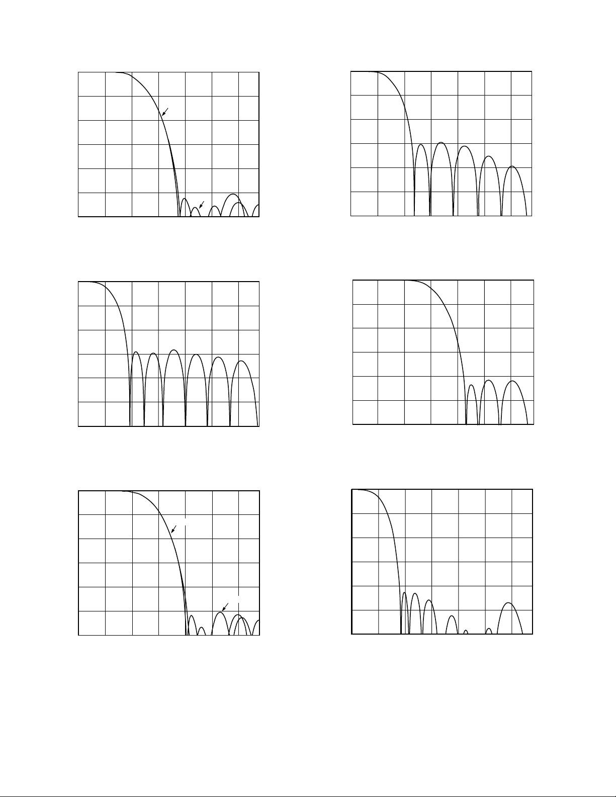
The Y filter supports several different frequency responses,
including two 4.5 MHz/5.0 MHz low pass responses, PAL/
NTSC subcarrier notch responses and a PAL/NTSC extended
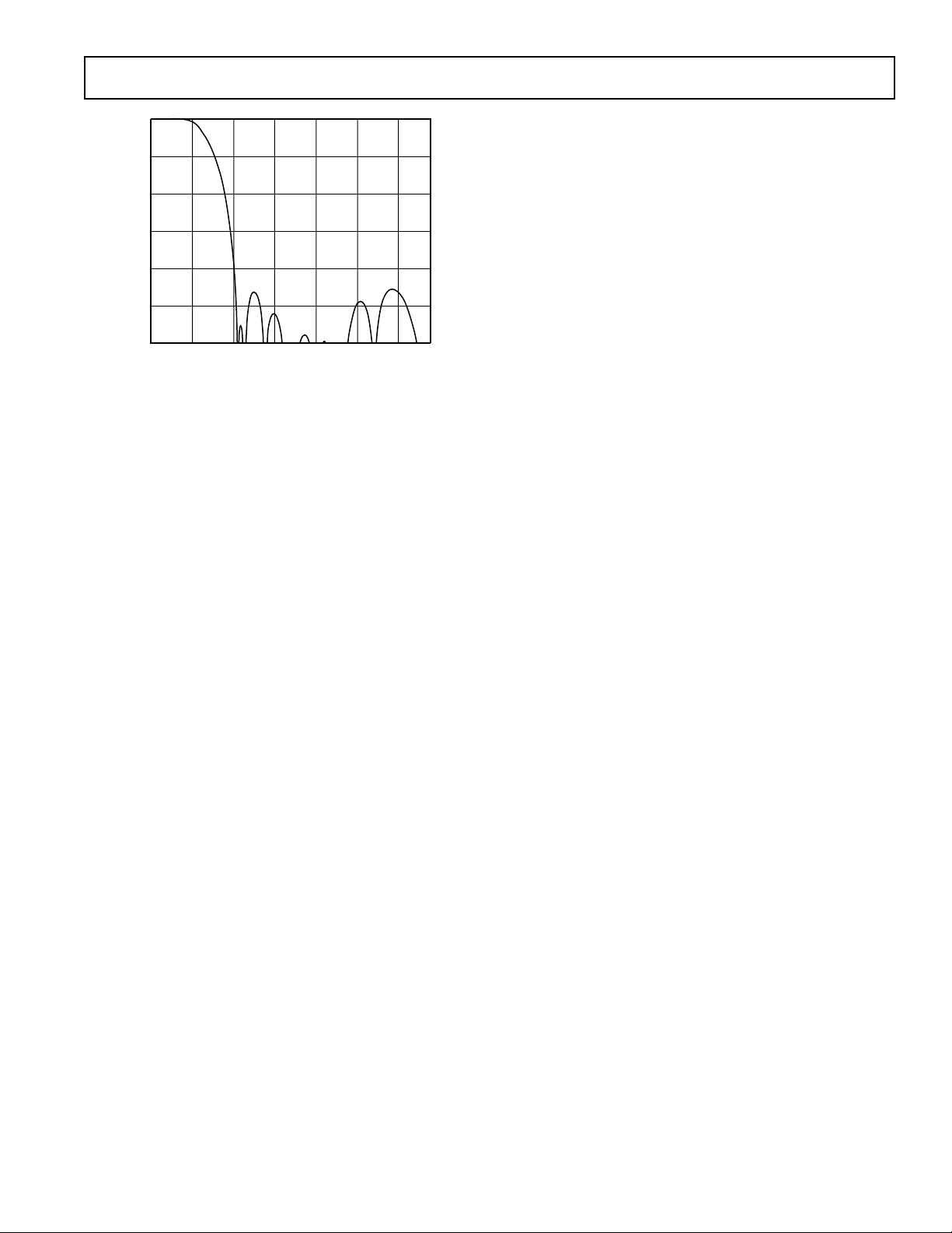
response. The U and V filters have a 2/2.4 MHz low-pass
response for NTSC/PAL. These filter characteristics are illustrated in Figures 4 to 12.
PASSBAND
FILTER SELECTION
MR04 MR03
NTSC 0 0 2.3 0.026 7.0
PAL 0 0 3.4 0.098 7.3
NTSC 0 1 1.0 0.085 3.57
PAL 0 1 1.4 0.107 4.43
NTSC/PAL 1 0 4.0 0.150 7.5
NTSC 1 1 2.3 0.054 7.0
PAL 1 1 3.4 0.106 7.3
CUTOFF (MHz)
PASSBAND
RIPPLE (dB)
STOPBAND
CUTOFF (MHz)
Figure 4. Luminance Internal Filter Specifications
PASSBAND
FILTER SELECTION
NTSC 1.0 0.085 3.2
PAL 1.3 0.04 4.0
CUTOFF (MHz)
PASSBAND
RIPPLE (dB)
STOPBAND
CUTOFF (MHz)
STOPBAND
ATTENUATION (dB)
Figure 5. Chrominance Internal Filter Specifications
–11–REV. B
STOPBAND
ATTENUATION (dB)
>
54 4.2
>
50 5.0
>
27.6 2.1
>
29.3 2.7
>
40 5.65
>
54 4.2
>
50.3 5.0
>
40 0.3 2.05
>
40 0.02 2.45
F
3dB
ATTENUATION @
1.3MHz (dB)
F
3dB
ADV7175A/ADV7176A
0
0
–10
–20
–30
AMPLITUDE – dB
–40
–50
–60
02468 1210
TYPE A
FREQUENCY – MHz
Figure 6. NTSC Low-Pass Filter
0
–10
–20
–30
AMPLITUDE – dB
–40
TYPE B
–10
–20
–30
AMPLITUDE – dB
–40
–50
–60
0 246 8 1210
FREQUENCY – MHz
Figure 9. PAL Notch Filter
–10
–20
–30
AMPLITUDE – dB
–40
–50
–60
0 246 8 1210
FREQUENCY – MHz
Figure 7. NTSC Notch Filter
0
–10
–20
–30
AMPLITUDE – dB
–40
–50
–60
0 246 8 1210
TYPE B
FREQUENCY – MHz
Figure 8. PAL Low-Pass Filter
TYPE A
–50
–60
0 246 8 1210
FREQUENCY – MHz
Figure 10. NTSC/PAL Extended Mode Filter
0
–10
–20
–30
AMPLITUDE – dB
–40
–50
–60
0 246 8 1210
FREQUENCY – MHz
Figure 11. NTSC UV Filter
–12–
REV. B
ADV7175A/ADV7176A
0
–10
–20
–30
AMPLITUDE – dB
–40
–50
–60
02468 1210
FREQUENCY – MHz
Figure 12. PAL UV Filter
COLOR BAR GENERATION
The ADV7175A/ADV7176A can be configured to generate
75% amplitude, 75% saturation (75/7.5/75/7.5) for NTSC or
75% amplitude, 100% saturation (100/0/75/0) for PAL color
bars. These are enabled by setting MR17 of Mode Register 1 to
Logic “1.”
SQUARE PIXEL MODE
The ADV7175A/ADV7176A can be used to operate in square
pixel mode. For NTSC operation an input clock of 24.5454
MHz is required. Alternatively an input clock of 29.5 MHz is
required for PAL operation. The internal timing logic adjusts
accordingly for square pixel mode operation.
COLOR SIGNAL CONTROL
The color information can be switched on and off the video
output using Bit MR24 of Mode Register 2.
BURST SIGNAL CONTROL
The burst information can be switched on and off the video
output using Bit MR25 of Mode Register 2.
NTSC PEDESTAL CONTROL
The pedestal on both odd and even fields can be controlled on a
line by line basis using the NTSC Pedestal Control Registers.
This allows the pedestals to be controlled during the vertical
blanking interval (Lines 10 to 25 and Lines 273 to 288).
PIXEL TIMING DESCRIPTION
The ADV7175A/ADV7176A can operate in either 8-bit or
16-bit YCrCb Mode.
8-Bit YCrCb Mode
This default mode accepts multiplexed YCrCb inputs through
the P7-P0 pixel inputs. The inputs follow the sequence Cb0, Y0
Cr0, Y1 Cb1, Y2, etc. The Y, Cb and Cr data are input on a
rising clock edge.
16-Bit YCrCb Mode
This mode accepts Y inputs through the P7–P0 pixel inputs and
multiplexed CrCb inputs through the P15–P8 pixel inputs. The
data is loaded on every second rising edge of CLOCK. The inputs
follow the sequence Cb0, Y0 Cr0, Y1 Cb1, Y2, etc.
SUBCARRIER RESET
Together with the SCRESET/RTC PIN and Bits MR22 and
MR21 of Mode Register 2, the ADV7175A/ADV7176A can be
used in subcarrier reset mode. The subcarrier will reset to
Field 0 at the start of the following field when a low to high
transition occurs on this input pin.
REAL TIME CONTROL
Together with the SCRESET/RTC PIN and Bits MR22 and
MR21 of Mode Register 2, the ADV7175A/ADV7176A can be
used to lock to an external video source. The real time control
mode allows the ADV7175A/ADV7176A to automatically alter
the subcarrier frequency to compensate for line length variation.
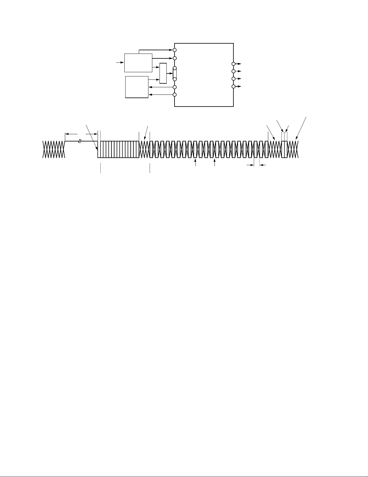
When the part is connected to a device that outputs a digital
datastream in the RTC format (such as an ADV7185 video
decoder [see Figure 13]), the part will automatically change to
the compensated subcarrier frequency on a line by line basis.
This digital datastream is 67 bits wide and the subcarrier is
contained in Bits 0 to 21. Each bit is two clock cycles long.
00HEX should be written to all four subcarrier frequency registers when using this mode.
VIDEO TIMING DESCRIPTION
The ADV7175A/ADV7176A is intended to interface to offthe-shelf MPEG1 and MPEG2 Decoders. Consequently, the
ADV7175A/ADV7176A accepts 4:2:2 YCrCb Pixel Data via a
CCIR-656 pixel port and has several video timing modes of
operation that allow it to be configured as either system master
video timing generator or a slave to the system video timing
generator. The ADV7175A/ADV7176A generates all of the
required horizontal and vertical timing periods and levels for the
analog video outputs.
The ADV7175A/ADV7176A calculates the width and placement of analog sync pulses, blanking levels and color burst
envelopes. Color bursts are disabled on appropriate lines, and
serration and equalization pulses are inserted where required.
In addition the ADV7175A/ADV7176A supports a PAL or
NTSC square pixel operation in slave mode. The part requires
an input pixel clock of 24.5454 MHz for NTSC and an input
pixel clock of 29.5 MHz for PAL. The internal horizontal line
counters place the various video waveform sections in the correct location for the new clock frequencies.
The ADV7175A/ADV7176A has four distinct master and four
distinct slave timing configurations. Timing Control is established with the bidirectional SYNC, BLANK and FIELD/
VSYNC pins. Timing Mode Register 1 can also be used to vary
the timing pulsewidths and where they occur in relation to each
other.
–13–REV. B
ADV7175A/ADV7176A
COMPOSITE
OR CABLE
VIDEO
e.g., VCR
VIDEO
DECODER
(e.g., ADV7185)
MPEG
DECODER
CLOCK
SCRESET/RTC
M
U
P7–P0
X
BLUE/COMPOSITE/U
HSYNC
FIELD/VSYNC
ADV7175A/ADV7176A
GREEN/LUMA/Y
RED/CHROMA/V
COMPOSITE
H/LTRANSITION
COUNT START
RTC
TIME SLOT: 01
NOTES:
1
FSC PLL INCREMENT IS 22 BITS LONG, VALUED LOADED INTO ADV7175A/ADV7176A FSC DDS REGISTER IS
F
PLL INCREMENTS BITS 21:0 PLUS BITS 0:9 OF SUB CARRIER FREQUENCY REGISTERS. ALL ZEROS SHOULD
SC
BE WRITTEN TO THE SUB CARRIER FREQUENCY REGISTERS OF THE ADV7175A/ADV7176A.
2
SEQUENCE BIT
PAL: 0 = LINE NORMAL, 1 = LINE INVERTED
NTSC: 0 = NO CHANGE.
3
RESET BIT
RESET ADV7175A/ADV7176A’s DDS.
128
LOW
14 BITS
RESERVED
13
NOT USED IN
ADV7175A/ADV7176A
0
14
4 BITS
RESERVED
21
19
FSCPLL INCREMENT
VALID
SAMPLE
INVALID
SAMPLE
SEQUENCE
2
5 BITS
RESERVED
1
8/LLC
BIT
0
6768
RESET
BIT
RESERVED
3
Figure 13. RTC Timing and Connections
Vertical Blanking Data Insertion
It is possible to allow encoding of incoming YCbCr data on those lines of VBI that do not bear line sync or pre/post-equalization
pulses (see Figures 15 to 26). This mode of operation is called “Partial Blanking” and is selected by setting MR31 to 1. It allows the
insertion of any VBI data (Opened VBI) into the encoded output waveform. This data is present in digitized incoming YCbCr data
stream (e.g., WSS data, CGMS, VPS, etc.). Alternatively, the entire VBI may be blanked (no VBI data inserted) on these lines by
setting MR31 to 0.
The complete VBI comprises of the following lines:
525/60 Systems, Lines 525 to 21 for Field 1 and Lines 262 to Line 284 for Field 2.
625/50 Systems, Lines 624 to Line 22 and Lines 311 to 335.
The “Opened VBI” consists of:
525/60 Systems, Lines 10 to 21 for Field 1 and second half of Line 273 to Line 284 for Field 2.
625/50 Systems, Line 7 to Line 22 and Lines 319 to 335.
Mode 0 (CCIR-656): Slave Option
(Timing Register 0 TR0 = X X X X X 0 0 0)
The ADV7175A/ADV7176A is controlled by the SAV (Start Active Video) and EAV (End Active Video) time codes in the pixel
data. All timing information is transmitted using a 4-byte synchronization pattern. A synchronization pattern is sent immediately
before and after each line during active picture and retrace. Mode 0 is illustrated in Figure 14. The HSYNC, FIELD/VSYNC and
BLANK (if not used) pins should be tied high during this mode.
–14–
REV. B
ANALOG
VIDEO
ADV7175A/ADV7176A
INPUT PIXELS
NTSC/PAL M SYSTEM
(525 LlNES/60Hz)
PAL SYSTEM
(625 LINES/50Hz)
EAV CODE
C
FF0000X
Y
Y
r
4 CLOCK
4 CLOCK 4 CLOCK
END OF ACTIVE
VIDEO LINE
8
10801
0
Y
0
FF00FFABABA
ANCILLARY DATA
268 CLOCK
280 CLOCK
B
(HANC)
801
8
0
0
SAV CODE
10FF0
0
XYC
Y
0
0
b
4 CLOCK
START OF ACTIVE
VIDEO LINE
1440 CLOCK
1440 CLCOK
C
C
C
C
Y
Y
Y
b
r
b
r
Figure 14. Timing Mode 0 (Slave Mode)
Mode 0 (CCIR-656): Master Option
(Timing Register 0 TR0 = X X X X X 0 0 1)
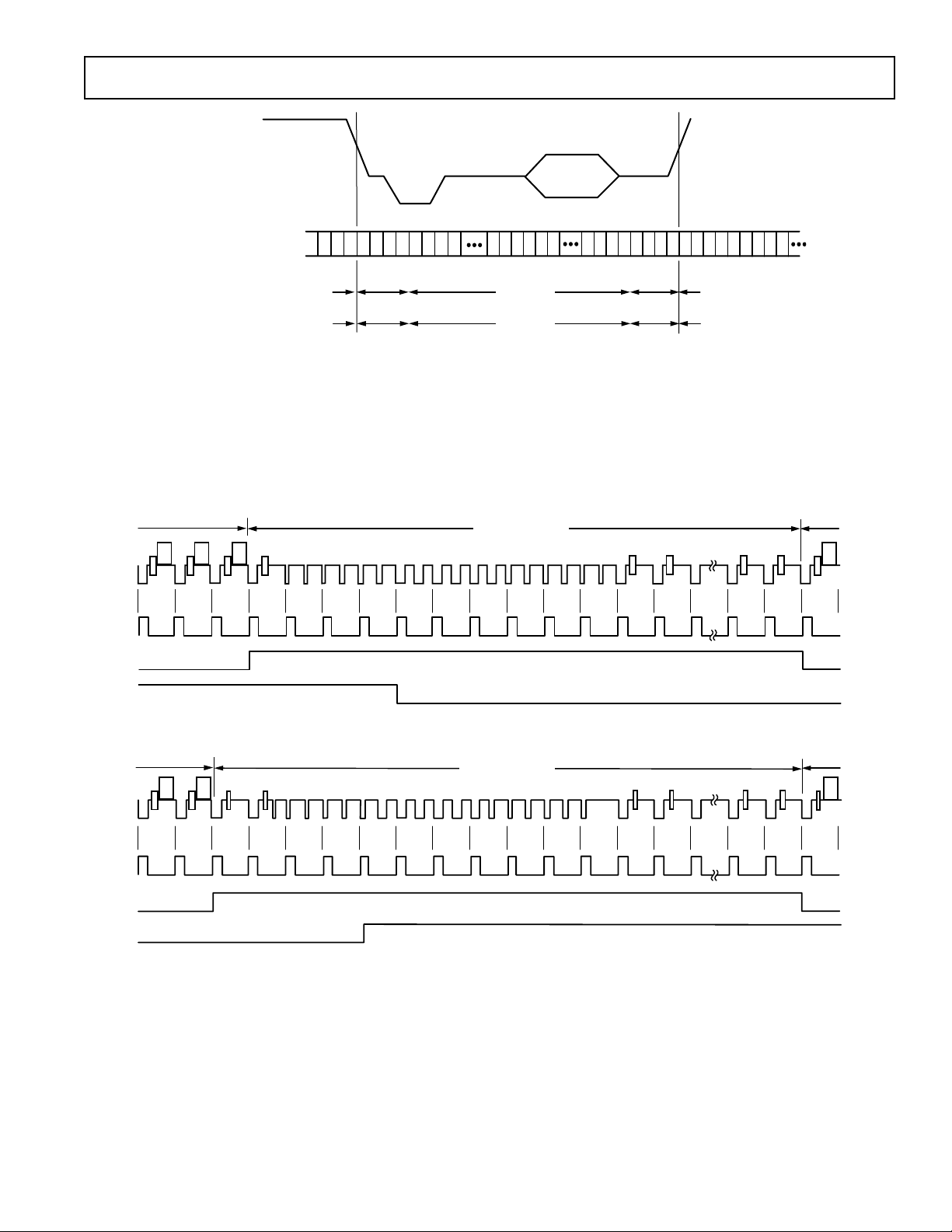
The ADV7175A/ADV7176A generates H, V and F signals required for the SAV (Start Active Video) and EAV (End Active Video)
time codes in the CCIR-656 standard. The H bit is output on the HSYNC pin, the V bit is output on the BLANK pin, and the F bit
is output on the FIELD/VSYNC pin. Mode 0 is illustrated in Figure 15 (NTSC) and Figure 16 (PAL). The H, V and F transitions
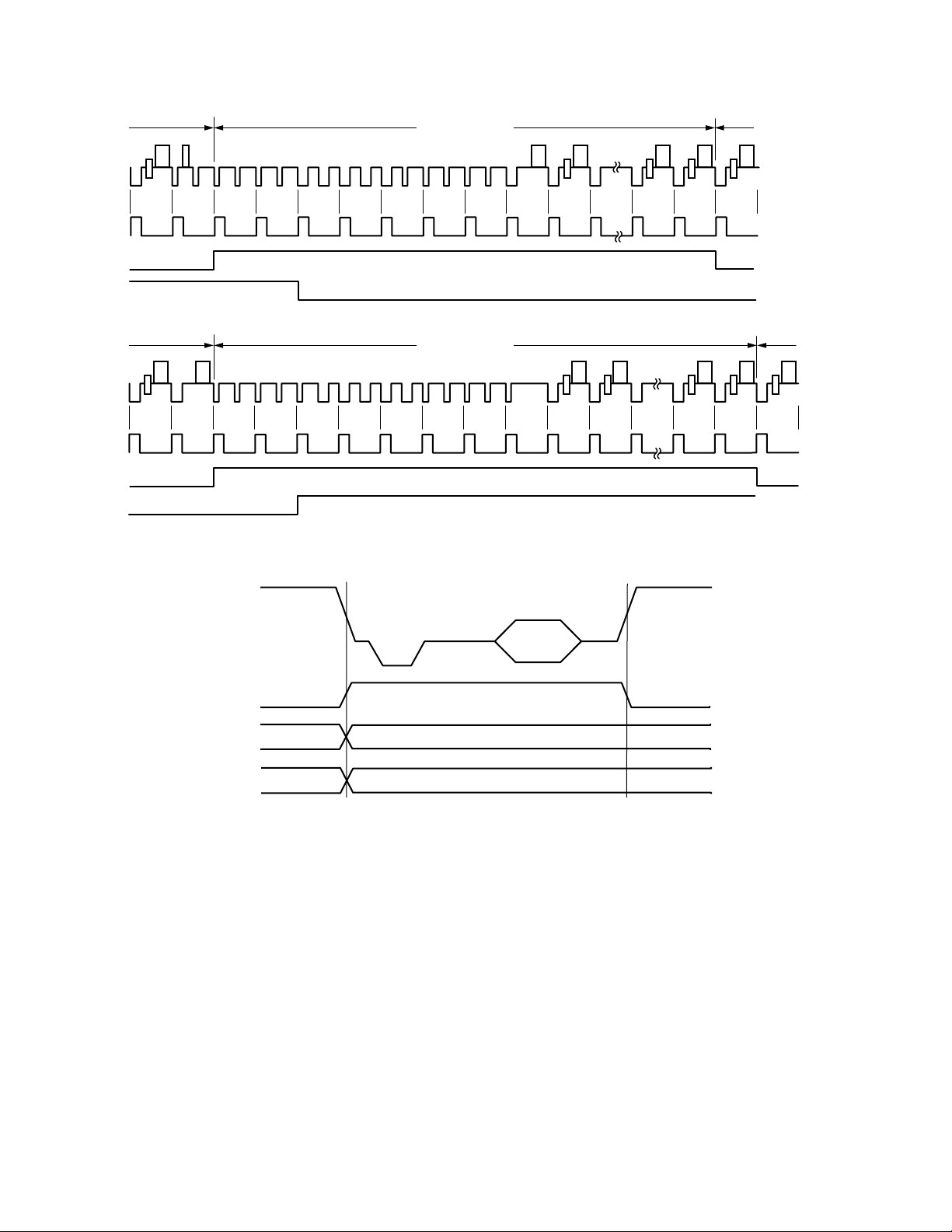
relative to the video waveform are illustrated in Figure 17.
DISPLAY
522 523 524 525 1 2 3 4
H
V
VERTICAL BLANK
67
5
8
10 11 20 21 22
9
DISPLAY
F
DISPLAY
260 261 262 263 264 265 266 267 268 269 270 271 272 273 274
H
V
F
ODD FIELD
ODD FIELDEVEN FIELD
VERTICAL BLANK
EVEN FIELD
Figure 15. Timing Mode 0 (NTSC Master Mode)
283
284
DISPLAY
285
–15–REV. B
ADV7175A/ADV7176A
DISPLAY
622 623 624 625 1 2 3 4
H
V
F
DISPLAY
309 310 311 312 314 315 316 317
H
V
F
ODD FIELD EVEN FIELD
ODD FIELDEVEN FIELD
313
Figure 16. Timing Mode 0 (PAL Master Mode)
VERTICAL BLANK
5
VERTICAL BLANK
67
318
319 320
DISPLAY
22 23
21
DISPLAY
335 336
334
ANALOG
VIDEO
H
F
V
Figure 17. Timing Mode 0 Data Transitions (Master Mode)
Mode 1: Slave Option HSYNC, BLANK, FIELD
(Timing Register 0 TR0 = X X X X X 0 1 0)
In this mode the ADV7175A/ADV7176A accepts horizontal SYNC and Odd/Even FIELD signals. A transition of the FIELD input
when HSYNC is low indicates a new frame i.e., vertical retrace. The BLANK signal is optional. When the BLANK input is disabled
the ADV7175A/ADV7176A automatically blanks all normally blank lines. Mode 1 is illustrated in Figure 18 (NTSC) and Figure 19 (PAL).
–16–
REV. B
 Loading...