现货库存、技术资料、百科信息、热点资讯,精彩尽在鼎好!
Chip Scale PAL/NTSC Video Encoder with
FEATURES
1
ITU-R
BT601/BT656 YCrCb to PAL/NTSC video encoder
High quality 10-bit video DACs
SSAF™ (super sub-alias filter)
Advanced power management features
CGMS (copy generation management system)
WSS (wide screen signaling)
NTSC M, PAL N
Single 27 MHz clock required (×2 oversampling)
Macrovision 7.1 (ADV7174 only)
80 dB video SNR
32-bit direct digital synthesizer for color subcarrier
Multistandard video output support:
Composite (CVBS)
Component S-video (Y/C)
Video input data port supports:
CCIR-656 4:2:2 8-bit parallel input format
Programmable simultaneous composite and S-video or RGB
(SCART)/YPbPr video outputs
Programmable luma filters low-pass [PAL/NTSC] notch,
extended SSAF, CIF, and QCIF
Programmable chroma filters (low-pass [0.65 MHz, 1.0 MHz,
1.2 MHz, and 2.0 MHz], CIF, and QCIF)
Programmable VBI (vertical blanking interval)
2
, PAL B/D/G/H/I, PAL-M3 , PAL 60
POWER
MANAGEMENT
V
RESET
COLOR
DATA
P7–P0
HSYNC
FIELD/VSYNC
BLANK
AA
CONTROL
(SLEEP MODE)
4:2:2 TO
4:4:4
INTER-
POLATOR
VIDEO TIMING
GENERATOR
8
8
8
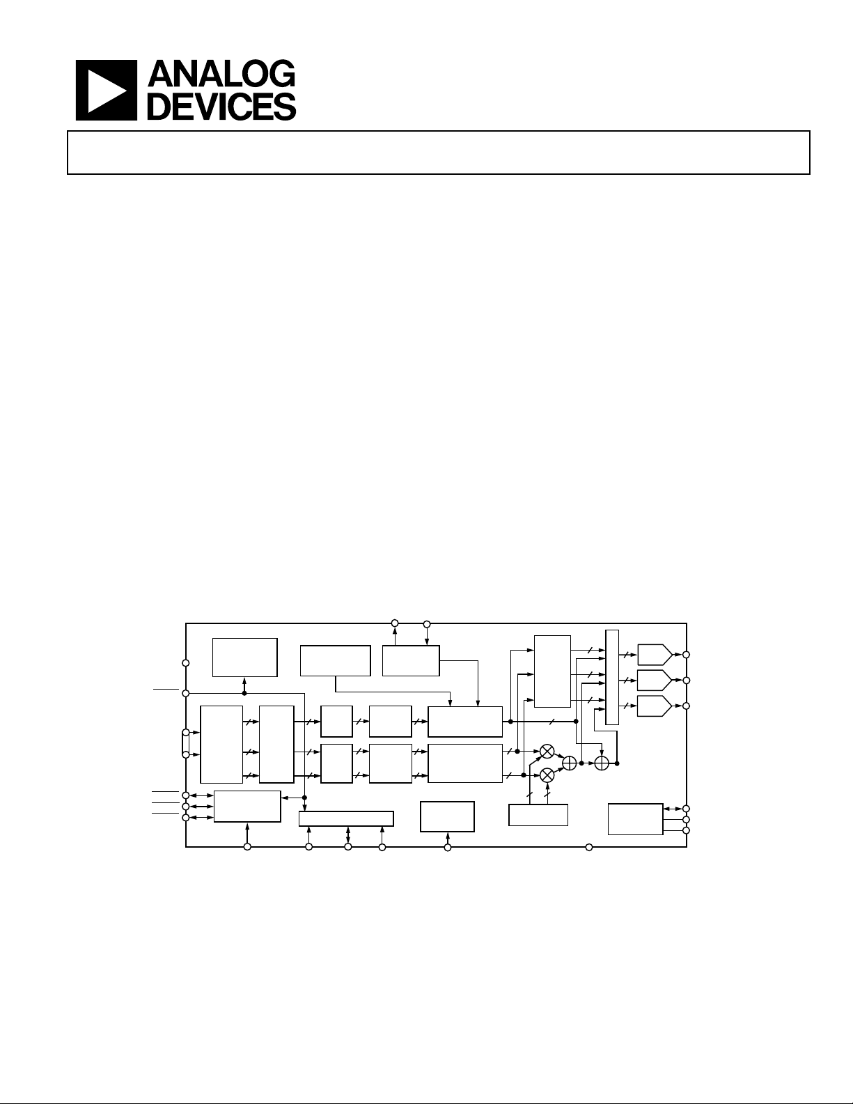
ADV7174/ADV7179
CGMS AND WSS
INSERTION
BLOCK
8
Y
YCrCb
TO
U
YUV
MATRIX
V
8
I2C MPU PORT
FUNCTIONAL BLOCK DIAGRAM
TTXREQ TTX
TELETEXT
INSERTION
BLOCK
9
ADD
SYNC
ADD
BURST
88
8
INTER-
POLATOR
INTER-
POLATOR
PROGRAMMABLE
9
LUMINANCE
FILTER
8
PROGRAMMABLE
CHROMINANCE
8
FILTER
REAL-TIME
CONTROL
CIRCUIT
Advanced Power Management
ADV7174/ADV7179
Programmable subcarrier frequency and phase
Programmable LUMA delay
Individual on/off control of each DAC
CCIR and square pixel operation
Integrated subcarrier locking to external video source
Color signal control/burst signal control
Interlaced/noninterlaced operation
Complete on-chip video timing generator
Programmable multimode master/slave operation
Closed captioning support
Teletext insertion port (PAL-WST)
On-board color bar generation
On-board voltage reference
2-wire serial MPU interface (I
Single-supply 2.8 V and 3.3 V operation
Small 40-lead 6 mm × 6 mm LFCSP package
−40°C to +85°C at 3.3 V
−20°C to +85°C at 2.8 V
APPLICATIONS
Portable video applications
Mobile phones
Digital still cameras
YUV TO
RBG
MATRIX
10
10
U
10
V
10
10
SIN/COS
DDS BLOCK
10
10
10
2
C® compatible and fast I2C)
M
U
10
10-BIT
L
DAC
T
I
10
10-BIT
P
DAC
L
E
10
X
10-BIT
E
DAC
R
VOLTAGE
REFERENCE
CIRCUIT
DACA(PIN29)
DACB(PIN28)
DACC(PIN24)
V
REF
R
SET
COMP
CLOCK
SCLOCK SDATA ALSB
SCRESET/RTC
GND
Figure 1.
1
ITU-R and CCIR are used interchangeably in this document (ITU-R has replaced CCIR recommendations).
2
Throughout the document, N is referenced to PAL – Combination – N.
3
ADV7174 only.
Protected by U.S. Patent Numbers 5,343,196 and 5,442,355 and other intellectual property rights.
Protected by U.S. Patent Numbers 4,631,603, 4,577,216, 4,819,098 and other intellectual property rights. The Macrovision anticopy process is licensed for
noncommercial home use only, which is its sole intended use in the device. Contact the sales office for the latest Macrovision version available.
Rev. A
Information furnished by Analog Devices is believed to be accurate and reliable.
However, no responsibility is assumed by Analog Devices for its use, nor for any
infringements of patents or other rights of third parties that may result from its use.
Specifications subject to change without notice. No license is granted by implication
or otherwise under any patent or patent rights of Analog Devices. Trademarks and
registered trademarks are the property of their respective owners.
One Technology Way, P.O. Box 9106, Norwood, MA 02062-9106, U.S.A.
Tel: 781.329.4700 www.analog.com
Fax: 781.326.8703 © 2004 Analog Devices, Inc. All rights reserved.
02980-A-001

ADV7174/ADV7179
TABLE OF CONTENTS
Specifications..................................................................................... 4
2.8 V Specifications ...................................................................... 4
2.8 V Timing Specifications ........................................................ 5
3.3 V Specifications ...................................................................... 6
3.3 V Timing Specifications ........................................................ 7
Absolute Maximum Ratings............................................................ 9
ESD Caution.................................................................................. 9
Pin Configuration and Function Descriptions........................... 10
General Description ....................................................................... 11
Data Path Description................................................................ 11
Internal Filter Response............................................................. 11
Typical Performance Characteristics ...........................................13
Features............................................................................................ 16
Color Bar Generation ................................................................ 16
Square Pixel Mode...................................................................... 16
Mode 3: Master/Slave Option
Power-On Reset .......................................................................... 25
SCH Phase Mode........................................................................ 25
MPU Port Description............................................................... 25
Register Accesses ........................................................................ 26
Register Programming................................................................... 27
Subaddress Register (SR7–SR0) ............................................... 27
Register Select (SR5–SR0)......................................................... 27
Mode Register 1 (MR1)............................................................. 29
Mode Register 2 (MR2)............................................................. 30
Mode Register 3 (MR3)............................................................. 31
Mode Register 4 (MR4)............................................................. 32
Timing Mode Register 0 (TR0) ................................................ 33
Timing Mode Register 1 (TR1) ................................................ 34
Subcarrier Frequency Registers 3–0 ........................................ 35
HSYNC, BLANK
, FIELD .. 24
Color Signal Control.................................................................. 16
Burst Signal Control................................................................... 16
NTSC Pedestal Control ............................................................. 16
Pixel Timing Description .......................................................... 16
8-Bit YCrCb Mode ................................................................. 16
Subcarrier Reset.......................................................................... 16
Real-Time Control ..................................................................... 16
Video Timing Description.................................................... 16
Vertical Blanking Data Insertion.......................................... 17
Mode 0 (CCIR-656): Slave Option....................................... 17
Mode 0 (CCIR-656): Master Option ................................... 17
Mode 1: Slave Option
Mode 1: Master Option
Mode 2: Slave Option
Mode 2: Master Option
HSYNC, BLANK
HSYNC, BLANK
HSYNC, VSYNC, BLANK
HSYNC, VSYNC, BLANK
, FIELD................ 20
, FIELD ............ 21
.............. 22
.......... 23
Subcarrier Phase Register.......................................................... 35
Closed Captioning Even Field Data Registers 1–0 ................ 35
Closed Captioning Odd Field Data Registers 1–0 ................. 36
NTSC Pedestal/PAL Teletext Control Registers 3–0 ............. 36
Teletext Request Control Register (TC07).............................. 37
CGMS_WSS Register 0 (C/W0)............................................... 37
CGMS_WSS Register 1 (C/W1)............................................... 38
CGMS_WSS Register 2 (C/W2)............................................... 38
Appendix 1—Board Design and Layout Considerations.......... 39
Ground Planes ............................................................................ 39
Power Planes ............................................................................... 39
Supply Decoupling..................................................................... 40
Digital Signal Interconnect ....................................................... 40
Analog Signal Interconnect....................................................... 40
Appendix 2—Closed Captioning ................................................. 41
Rev. A | Page 2 of 52

ADV7174/ADV7179
Appendix 3—Copy Generation Management System (CGMS)
............................................................................................................42
Function of CGMS Bits..............................................................42
Appendix 4—Wide Screen Signaling (WSS) ...............................43
Function of WSS Bits ..................................................................43
Appendix 5—Teletext .....................................................................44
Teletext Insertion.........................................................................44
Teletext Protocol..........................................................................44
Appendix 6—Waveforms ...............................................................45
NTSC Waveforms (with Pedestal) ............................................45
REVISION HISTORY
2/04—Changed from REV. 0 to REV A.
Added 2.8 V Version.......................................................... Universal
NTSC Waveforms (without Pedestal) ......................................46
PAL Waveforms...........................................................................47
Pb Pr Waveforms.........................................................................48
Appendix 7—Optional Output Filter...........................................49
Appendix 8—Recommended Register Values.............................50
Outline Dimensions........................................................................52
Ordering Guide ...........................................................................52
Format Updated.................................................................. Universal
Device Currents Updated on 3.3 V Specification .......... Universal
Added new Table 1 and Renumbered Subsequent Tables.............4
Added new Table 2 and Renumbered Subsequent Tables ...........5
Change to Figure 54........................................................................38
Change to Figure 55........................................................................39
Change to Figure 79........................................................................48
Changed Ordering Guide Temperature Specifications ..............52
Updated Outline Dimensions........................................................52
10/02—Revision 0: Initial Version
Rev. A | Page 3 of 52

ADV7174/ADV7179
SPECIFICATIONS
2.8 V SPECIFICATIONS
V
= 2.8 V, V
AA
= 1.235 V, R
REF
= 150 Ω. All specifications T
SET
MIN
to T
Table 1.
Parameter Conditions1 Min Typ Max Unit
STATIC PERFORMANCE2
Resolution (Each DAC) 10 Bits
Accuracy (Each DAC)
Integral Nonlinearity R
= 300 Ω ±3.0 LSB
SET
Differential Nonlinearity Guaranteed monotonic ±1 LSB
DIGITAL INPUTS2
Input High Voltage, V
Input Low Voltage, V
Input Current, IIN V
Input Capacitance, C
1.6 V
INH
0.7 V
INL
= 0.4 V or 2.4 V ±1 µA
IN
10 pF
IN
DIGITAL OUTPUTS2
Output High Voltage, VOH I
Output Low Voltage, VOL I
= 400 µA 2.4 V
SOURCE
= 3.2 mA 0.4 V
SINK
Three-State Leakage Current 10 µA
Three-State Output Capacitance 10 pF
ANALOG OUTPUTS2
Output Current 3 R
= 150 Ω, RL = 37.5 Ω 33 34.7 37 mA
SET
DAC-to-DAC Matching 2.0 %
Output Compliance, VOC 0 1.4 V
Output Impedance, R
Output Capacitance, C
POWER REQUIREMENTS
30 kΩ
OUT
I
OUT
2, 4
= 0 mA 30 pF
OUT
VAA 2.8 V
Normal Power Mode
I
(Max)5 R
DAC
6
I
30 mA
CCT
= 150 Ω, RL = 37.5 Ω 115 120 mA
SET
Low Power Mode
I
(Max)5 62 mA
DAC
6
I
30 mA
CCT
Sleep Mode
7
I
0.1 µA
DAC
8
I
0.001 µA
CCT
Power Supply Rejection Ratio COMP = 0.1 µF 0.01 0.5 %/%
1
Temperature range T
2
Guaranteed by characterization.
3
DACs can output 35 mA typically at 2.8 V (R
4
Power measurements are taken with clock frequency = 27 MHz. Max TJ = 110°C.
5
I
is the total current (min corresponds to 5 mA output per DAC, max corresponds to 37 mA output per DAC) to drive all three DACs. Turning off individual DACs
DAC
reduces I
6
I
CCT
7
Total DAC current in sleep mode.
8
Total continuous current during sleep mode.
correspondingly.
DAC
(circuit current) is the continuous current required to drive the device.
to T
MIN
: –20°C to +85°C.
MAX
= 150 Ω and RL = 37.5 Ω). Full drive into 37.5 Ω load.
SET
1
, unless other wise noted.
MAX
Rev. A | Page 4 of 52

ADV7174/ADV7179
2.8 V TIMING SPECIFICATIONS
VAA = 2.8 V, V
= 1.235 V, R
REF
= 150 Ω. All specifications T
SET
MIN
to T
Table 2.
Parameter Conditions1 Min Typ Max Unit
MPU PORT
2, 3
SCLOCK Frequency 0 400 kHz
SCLOCK High Pulse Width, t1 0.6 µs
SCLOCK Low Pulse Width, t2 1.3 µs
Hold Time (Start Condition), t3 After this period the first clock is generated 0.6 µs
Setup Time (Start Condition), t4 Relevant for repeated start condition 0.6 µs
Data Setup Time, t5 100 ns
SDATA, SCLOCK Rise Time, t6 300 ns
SDATA, SCLOCK Fall Time, t7 300 ns
Setup Time (Stop Condition), t8 0.6 µs
ANALOG OUTPUTS
3, 4
Analog Output Delay 7 ns
DAC Analog Output Skew 0 ns
CLOCK CONTROL AND PIXEL PORT
f
27 MHz
CLOCK
4, 5
Clock High Time, t9 8 ns
Clock Low Time, t10 8 ns
Data Setup Time, t11 3.5 ns
Data Hold Time, t12 4 ns
Control Setup Time, t11 4 ns
Control Hold Time, t12 3 ns
Digital Output Access Time, t13 12 ns
Digital Output Hold Time, t
Pipeline Delay, t
TELETEXT
3, 4, 6
5
48 Clock Cycles
PD
4
8 ns
1
Digital Output Access Time, t16 23 ns
Data Setup Time, t17 2 ns
Data Hold Time, t18 6 ns
RESET
RESET
CONTROL
Low Time
3, 4
6 ns
1
Temperature range T
2
TTL input values are 0 V to 2.8 V, with input rise/fall times −3 ns, measured between the 10% and 90% points. Timing reference points at 50% for inputs and outputs.
Analog output load –10 pF.
3
Guaranteed by characterization.
4
Output delay measured from the 50% point of the rising edge of CLOCK to the 50% point of full-scale transition.
5
See Figure 60.
6
Teletext Port consists of the following:
Teletext Output: TTXREQ
Teletext Input: TTX
to T
MIN
: –20°C to +85°C.
MAX
1
, unless other wise noted.
MAX
Rev. A | Page 5 of 52

ADV7174/ADV7179
3.3 V SPECIFICATIONS
VAA = 3.0 V–3.6 V1, V
= 1.235 V, R
REF
= 150 Ω. All specifications T
SET
MIN
to T
Table 3.
Parameter Conditions1 Min Typ Max Unit
STATIC PERFORMANCE3
Resolution (Each DAC) 10 Bits
Accuracy (Each DAC)
Integral Nonlinearity R
= 300 Ω ± 0.6 LSB
SET
Differential Nonlinearity Guaranteed Monotonic ± 1 LSB
DIGITAL INPUTS3
Input High Voltage, V
Input Low Voltage, V
Input Current, I
IN
Input Capacitance, C
2 V
INH
0.8 V
INL
3, 4
V
10 pF
IN
= 0.4 V or 2.4 V ± 1 µA
IN
DIGITAL OUTPUTS3
Output High Voltage, VOH I
Output Low Voltage, VOL I
= 400 µA 2.4 V
SOURCE
= 3.2 mA 0.4 V
SINK
Three-State Leakage Current 10 µA
Three-State Output Capacitance 10 pF
ANALOG OUTPUTS3
Output Current
Output Current6 R
4, 5
R
= 150 Ω, RL = 37.5 Ω 33 34.7 37 mA
SET
= 1041 Ω, RL = 262.5 Ω 5 mA
SET
DAC-to-DAC Matching 2.0 %
Output Compliance, VOC 0 1.4 V
Output Impedance, R
Output Capacitance, C
POWER REQUIREMENTS
30 kΩ
OUT
I
OUT
3, 7
= 0 mA 30 pF
OUT
VAA 3.0 3.3 3.6 V
Normal Power Mode
I
(Max)8 R
DAC
I
(Min)8 R
DAC
9
I
35 mA
CCT
= 150 Ω, RL = 37.5 Ω 115 120 mA
SET
= 1041 Ω, RL = 262.5 Ω 20 mA
SET
Low Power Mode
I
(Max)8 62 mA
DAC
I
(Min)8 20 mA
DAC
9
I
35 mA
CCT
Sleep Mode
10
I
0.1 µA
DAC
11
I
0.001 µA
CCT
Power Supply Rejection Ratio COMP = 0.1 µF 0.01 0.5 %/%
1
The max/min specifications are guaranteed over this range. The max/min values are typical over 3.0 V to 3.6 V.
2
Temperature range T
3
Guaranteed by characterization.
4
Full drive into 37.5 Ω load.
5
DACs can output 35 mA typically at 3.3 V (R
6
Minimum drive current (used with buffered/scaled output load).
7
Power measurements are taken with clock frequency = 27 MHz. Max TJ = 110°C.
8
I
is the total current (min corresponds to 5 mA output per DAC, max corresponds to 37 mA output per DAC) to drive all three DACs. Turning off individual DACs
DAC
reduces I
9
I
CCT
10
Total DAC current in sleep mode.
11
Total continuous current during sleep mode.
correspondingly.
DAC
(circuit current) is the continuous current required to drive the device.
to T
MIN
: –40°C to +85°C.
MAX
= 150 Ω and RL = 37.5 Ω), optimum performance obtained at 18 mA DAC current (R
SET
2
, unless othe r wise noted.
MAX
= 300 Ω and RL = 75 Ω).
SET
Rev. A | Page 6 of 52

ADV7174/ADV7179
3.3 V TIMING SPECIFICATIONS
VAA = 3.0 V–3.6 V1, V
= 1.235 V, R
REF
= 150 Ω. All specifications T
SET
MIN
to T
Table 4.
Parameter Conditions1 Min Typ Max Unit
MPU PORT
3, 4
SCLOCK Frequency 0 400 kHz
SCLOCK High Pulse Width, t1 0.6 µs
SCLOCK Low Pulse Width, t2 1.3 µs
Hold Time (Start Condition), t3 After this period, the first clock is generated 0.6 µs
Setup Time (Start Condition), t4 Relevant for repeated start condition 0.6 µs
Data Setup Time, t5 100 ns
SDATA, SCLOCK Rise Time, t6 300 ns
SDATA, SCLOCK Fall Time, t7 300 ns
Setup Time (Stop Condition), t8 0.6 µs
ANALOG OUTPUTS
3, 5
Analog Output Delay 7 ns
DAC Analog Output Skew 0 ns
CLOCK CONTROL AND PIXEL PORT
f
27 MHz
CLOCK
4, 5
Clock High Time, t9 8 ns
Clock Low Time, t10 8 ns
Data Setup Time, t11 3.5 ns
Data Hold Time, t12 4 ns
Control Setup Time, t11 4 ns
Control Hold Time, t12 3 ns
Digital Output Access Time, t13 12 ns
Digital Output Hold Time, t14 8 ns
Pipeline Delay, t
TELETEXT
3, 4
6
48 Clock Cycles
PD
Digital Output Access Time, t16 23 ns
Data Setup Time, t17 2 ns
Data Hold Time, t18 6 ns
RESET
RESET
CONTROL
Low Time
3, 4
6 ns
1
The maximum/minimum specifications are guaranteed over this range. The maximum/minimum values are typical over 3.0 V to 3.6 V range.
2
Temperature range T
3
TTL input values are 0 V to 3 V, with input rise/fall times −3 ns, measured between the 10% and 90% points. Timing reference points at 50% for inputs and outputs.
Analog output load –10 pF.
4
Guaranteed by characterization.
5
Output delay measured from the 50% point of the rising edge of CLOCK to the 50% point of full-scale transition.
6
See Figure 60.
to T
MIN
: –40°C to +85°C.
MAX
2
, unless othe r wise noted.
MAX
Rev. A | Page 7 of 52
ADV7174/ADV7179
S
SDATA
CLOCK
CONTROL
I/PS
S
FIELD/VSYNC,
CLOCK
HSYNC,
BLANK
t
t
3
t
6
t
2
5
t
1
t
7
t
3
t
4
t
02980-0A-002
8
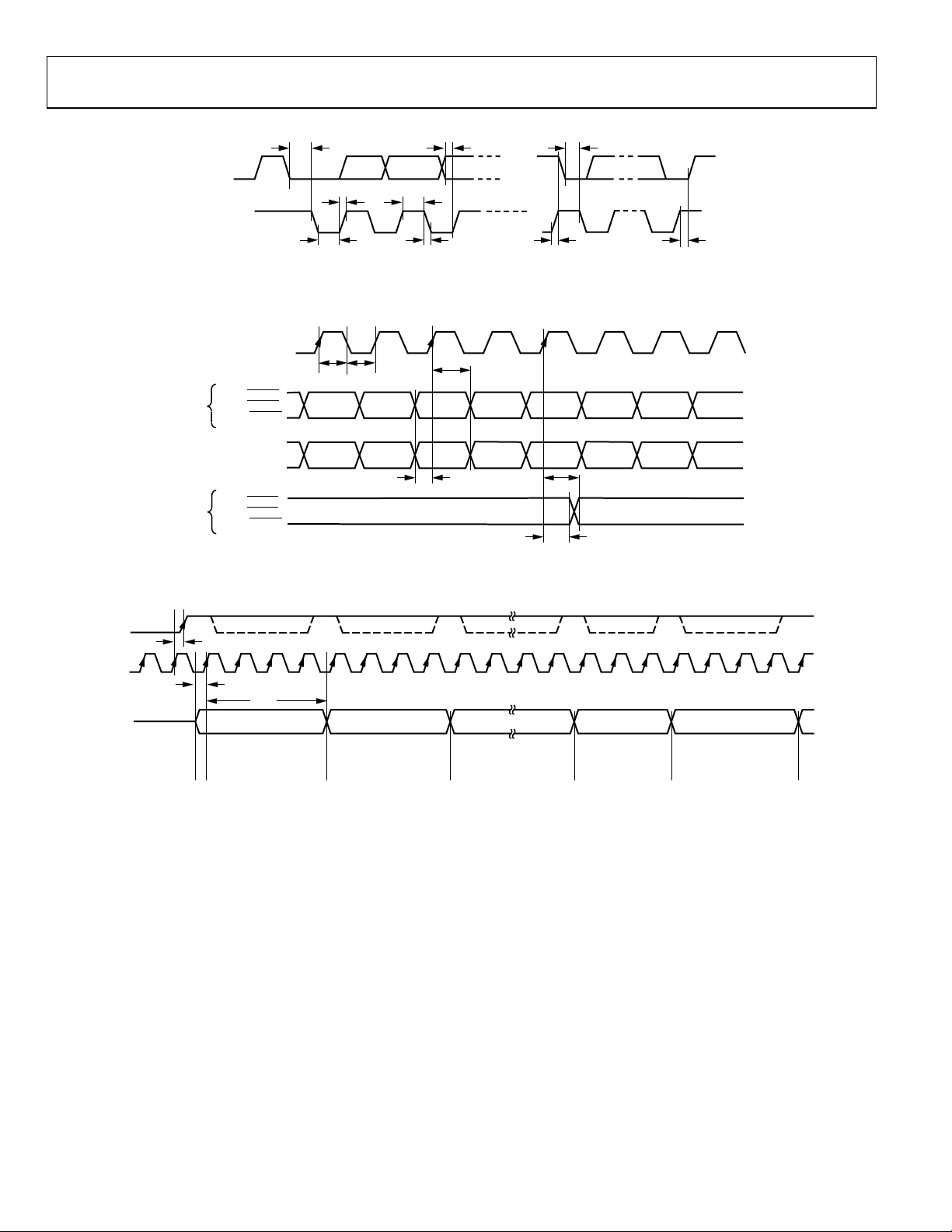
Figure 2. MPU Port Timing Diagram
t
t
9
10
t
12
CONTROL
O/PS
PIXEL INPUT
DATA
HSYNC,
FIELD/VSYNC,
BLANK
Cb Y Cr Y Cb Y
t
11
t
13
t
14
02980-A-003
Figure 3. Pixel and Control Data Timing Diagram
TTXREQ
t
16
CLOCK
t
17
TTX
t
18
4 CLOCK
CYCLES
4 CLOCK
CYCLES
4 CLOCK
CYCLES
3 CLOCK
CYCLES
4 CLOCK
CYCLES
02980-A-004
Figure 4. Teletext Timing Diagram
Rev. A | Page 8 of 52
ADV7174/ADV7179
ABSOLUTE MAXIMUM RATINGS
Table 5.
Parameter Rating
VAA to GND 4 V
Voltage on Any Digital Input Pin GND – 0.5 V to VAA + 0.5 V
Storage Temperature (TS) −65°C to +150°C
Junction Temperature (TJ) 150°C
Lead Temperature
260°C
Soldering, 10 sec
Analog Outputs to GND1 GND – 0.5 V to VAA
2
θ
JA
__________________________________________________
1
Analog output short circuit to any power supply or common can be of an indefinite duration.
2
With the exposed metal paddle on the underside of LFCSP soldered to GND on the PCB.
30°C/W
Stresses above those listed under Absolute Maximum Ratings
may cause permanent damage to the device. This is a stress
rating only; functional operation of the device at these or any
other conditions above those listed in the operational sections
of this specification is not implied. Exposure to absolute
maximum rating conditions for extended periods may affect
device reliability
ESD CAUTION
ESD (electrostatic discharge) sensitive device. Electrostatic charges as high as 4000 V readily accumulate on
the human body and test equipment and can discharge without detection. Although this product features
proprietary ESD protection circuitry, permanent damage may occur on devices subjected to high energy
electrostatic discharges. Therefore, proper ESD precautions are recommended to avoid performance
degradation or loss of functionality.
Rev. A | Page 9 of 52
ADV7174/ADV7179
C
K
PIN CONFIGURATION AND FUNCTION DESCRIPTIONS
SCRESET/
RTC
TTXREQ
AA
V
GND
SET
R
RESET
30
29
28
27
26
25
24
23
22
21
V
REF
DAC A
DAC B
V
AA
GND
V
AA
DAC C
COMP
SDATA
SCLOCK
02980-A-005
LOC
GND
GND
GND
GND
P3P2P1
GND
P4
39
40 33 32 3134
PIN 1
1
V
AA
P5
P6
P7
V
AA
INDICATOR
2
3
4
5
6
7
8
9
10
11
37 36 3538
ADV7174/ADV7179
LFCSP
TOP VIEW
(Not to Scale)
12 13 14 15 16 171819 20
GND
GND
HSYNC
FIELD/VSYNC
P0
ALSB
BLANK
TTX
GND
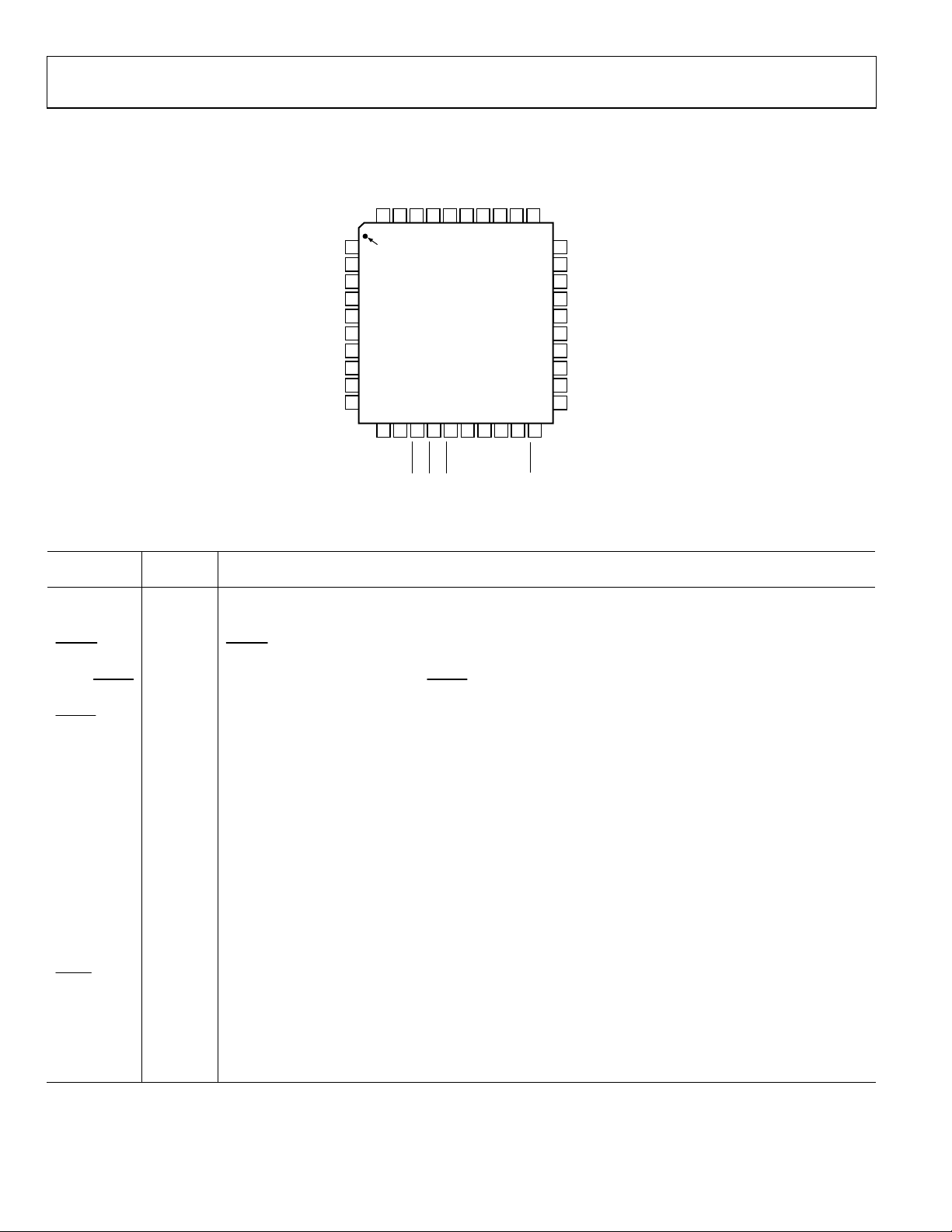
Figure 5. Pin Configurations
Table 6. Pin Function Descriptions
Input/
Mnemonic
Output
Function
P7–P0 I 8-Bit 4:2:2 Multiplexed YCrCb Pixel Port (P7–P0). P0 is the LSB.
CLOCK I
TTL Clock Input. Requires a stable 27 MHz reference clock for standard operation. Alternatively, a 24.5454 MHz
(NTSC) or 29.5 MHz (PAL) can be used for square pixel operation.
HSYNC
I/O
HSYNC
(Modes 1 and 2) Control Signal. This pin may be configured to output (master mode) or accept (slave
mode) sync signals.
FIELD/VSYNC
I/O
Dual Function FIELD (Mode 1) and VSYNC (Mode 2) Control Signal. This pin may be configured to output
(master mode) or accept (slave mode) these control signals.
BLANK
SCRESET/RTC I
I/O Video Blanking Control Signal. The pixel inputs are ignored when this is Logic 0. This signal is optional.
This pin can be configured as an input by setting MR22 and MR21 of Mode Register 2. It can be configured as a
subcarrier reset pin, in which case a low-to-high transition on this pin resets the subcarrier to Field 0.
Alternatively, it can be configured as a real-time control (RTC) input.
V
I/O Voltage Reference Input for DACs or Voltage Reference Output (1.235 V).
REF
R
I A 150 Ω resistor connected from this pin to GND is used to control full-scale amplitudes of the video signals.
SET
COMP O
Compensation Pin. Connect a 0.1 µF capacitor from COMP to V
. For optimum dynamic performance in low
AA
power mode, the value of the COMP capacitor can be lowered to as low as 2.2 nF.
DAC A O DAC Output (see Table 13)
DAC B O DAC Output (see Table 13).
DAC C O DAC Output (see Table 13).
SCLOCK I MPU Port Serial Interface Clock Input.
SDATA I/O MPU Port Serial Data Input/Output.
ALSB I TTL Address Input. This signal sets up the LSB of the MPU address.
RESET
I
This input resets the on-chip timing generator and sets the ADV7174/ADV7179 into default mode. This is NTSC
operation, Timing Slave Mode 0, 8-bit operation, 2× composite out signals. DACs A, B, and C are enabled.
TTX I Teletext Data.
TTXREQ O Teletext Data Request Signal/Defaults to GND when Teletext Not Selected.
VAA P Power Supply (2.8 V or 3.3 V).
GND G Ground Pin.
Rev. A | Page 10 of 52

ADV7174/ADV7179
GENERAL DESCRIPTION
The ADV7174/ADV7179 is an integrated digital video encoder
that converts digital CCIR-601 4:2:2 8-bit component video data
into a standard analog baseband television signal compatible
with worldwide standards.
The on-board SSAF (super sub-alias filter) with extended
luminance frequency response and sharp stop-band attenuation
enables studio quality video playback on modern TVs, giving
optimal horizontal line resolution.
typically have a range of 128 ± 112; however, it is possible to
input data from 1 to 254 on both Y, Cb, and Cr. The ADV7174/
ADV7179 supports PAL (B/D/G/H/I/M/N) and NTSC (with
and without pedestal) standards. The appropriate SYNC,
and burst levels are added to the YCrCb data. Macrovision Antitaping (ADV7174 only), closed-captioning, and Teletext levels
are also added to Y and the resultant data is interpolated to a
rate of 27 MHz. The interpolated data is filtered and scaled by
three digital FIR filters.
BLANK
,
An advanced power management circuit enables optimal control of power consumption in both normal operating modes
and in power-down or sleep modes.
The ADV7174/ADV7179 supports both PAL and NTSC square
pixel operation. The parts incorporate WSS and CGMS-A data
control generation.
The output video frames are synchronized with the incoming
data timing reference codes. Optionally, the encoder accepts
(and can generate)
These timing signals can be adjusted to change pulse width and
position while the part is in the master mode. The encoder
requires a signal two times the pixel rate (27 MHz) clock for
standard operation. Alternatively, the encoder requires a
24.5454 MHz clock for NTSC or 29.5 MHz clock for PAL
square pixel mode operation. All internal timing is generated
on-chip.
A separate Teletext port enables the user to directly input
Teletext data during the vertical blanking interval.
The ADV7174/ADV7179 modes are set up over a 2-wire serial
bidirectional port (I
The ADV7174/ADV7179 is packaged in a 40-lead 6 mm × 6 mm
LFCSP package.
HSYNC
2
VSYNC
,
C compatible) with two slave addresses.
, and FIELD timing signals.
DATA PATH DESCRIPTION
For PAL B/D/G/H/I/M/N and NTSC M and N modes, YCrCb
4:2:2 data is input via the CCIR-656 compatible pixel port at a
27 MHz data rate. The pixel data is demultiplexed to form three
data paths. Y typically has a range of 16 to 235, and Cr and Cb
The U and V signals are modulated by the appropriate subcarrier
sine/cosine phases and added together to make up the chrominance signal. The luma (Y) signal can be delayed 1–3 luma
cycles (each cycle is 74 ns) with respect to the chroma signal.
The luma and chroma signals are then added together to make
up the composite video signal. All edges are slew rate limited.
The YCrCb data is also used to generate RGB data with
appropriate SYNC and
synchronization with the composite video output. Alternatively,
analog YPbPr data can be generated instead of RGB data.
The three l0-bit DACs can be used to output:
• Composite Video + Composite Video
• S-Video + Composite Video
• YPrPb Video
• SCART RGB Video
Alternatively, each DAC can be individually powered off if not
required.
Video output levels are illustrated in Appendix 6.
BLANK
levels. The RGB data is in
INTERNAL FILTER RESPONSE
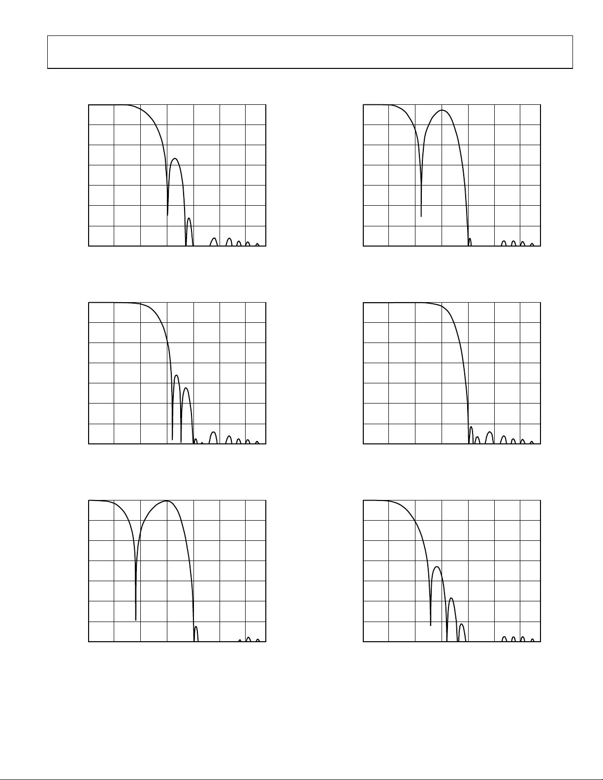
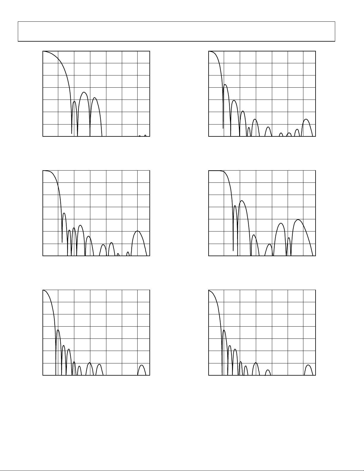
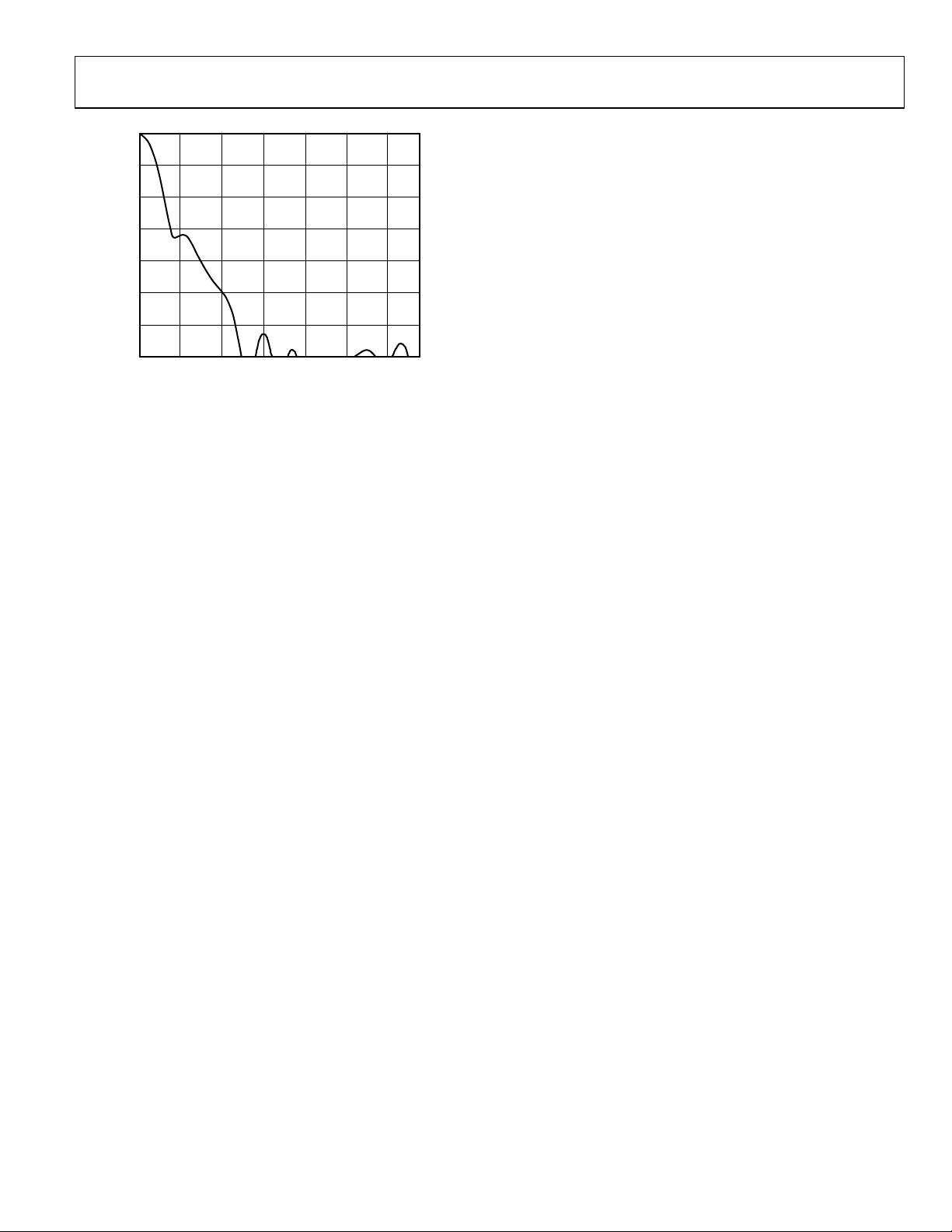
The Y filter supports several different frequency responses,
including two low-pass responses, two notch responses, an
extended (SSAF) response, a CIF response, and a QCIF
response. The UV filter supports several different frequency
responses, including four low-pass responses, a CIF response,
and a QCIF response. These can be seen in Table 7 and Table 8
and Figure 6 to Figure 18.
Rev. A | Page 11 of 52

ADV7174/ADV7179
Table 7. Luminance Internal Filter Specifications
Filter Type
Low-Pass
(NTSC)
Low-Pass
(PAL)
Notch (NTSC) 0 1 0 0.015 6.54 8.3 −68
Notch (PATL) 0 1 1 0.095 6.24 8.0 −66
Extended
(SSAF)
CIF 1 0 1 0.018 3.0 7.06 −61
QCIF 1 1 0 Monotonic 1.5 7.15 −50
Table 8. Chrominance Internal Filter Specifications
Filter Type
1.3 MHz
Low-Pass
0.65 MHz
Low-Pass
1.0 MHz
Low-Pass
2.0 MHz
Low-Pass
Reserved 1 0 0
CIF 1 0 1 0.084 0.7 3.01 −45
QCIF 1 1 0 Monotonic 0.5 4.08 −50
Filter Selection
MR04 MR03 MR02
0 0 0 0.091 4.157 7.37 −56
0 0 1 0.15 4.74 7.96 −64
1 0 0 0.051 6.217 8.0 −61
Filter Selection
MR07 MR06 MR05
0 0 0 0.084 1.395 3.01 −45
0 0 1 Monotonic 0.65 3.64 −58.5
0 1 0 Monotonic 1.0 3.73 −49
0 1 1 0.0645 2.2 5.0 −40
Pass-Band Ripple
(dB)
Pass-Band Ripple
(dB)
3 dB Bandwidth
(MHz)
3 dB Bandwidth
(MHz)
Stop-Band Cutoff
(MHz)
Stop-Band Cutoff
(MHz)
Stop-Band Attenuation
(dB)
Stop-Band Attenuation
(dB)
Rev. A | Page 12 of 52
ADV7174/ADV7179
TYPICAL PERFORMANCE CHARACTERISTICS
0
0
–10
–20
–30
–40
MAGNITUDE (dB)
–50
–60
–70
0122
46 810
FREQUENCY (MHz)
Figure 6. Chrominance Internal Filter Specifications
0
–10
–20
–30
–40
MAGNITUDE (dB)
–50
–10
–20
–30
–40
MAGNITUDE (dB)
–50
–60
02980-A-006
–70
0122
46 810
FREQUENCY (MHz)
02980-A-009
Figure 9. PAL Notch Luma Fil ter
0
–10
–20
–30
–40
MAGNITUDE (dB)
–50
–60
–70
–10
–20
–30
–40
MAGNITUDE (dB)
–50
–60
–70
0122
0
0122
46 810
FREQUENCY (MHz)
Figure 7. PAL Low-Pass Luma Filter
46 810
FREQUENCY (MHz)
Figure 8. NTSC Notch Luma Filter
–60
02980-A-007
–70
0122
46 810
FREQUENCY (MHz)
02980-A-010
Figure 10. Extended Mode (SSAF) Luma Filter
0
–10
–20
–30
–40
MAGNITUDE (dB)
–50
–60
02980-A-008
–70
0122
46 810
FREQUENCY (MHz)
02980-A-011
Figure 11. CIF Luma Filter
Rev. A | Page 13 of 52
ADV7174/ADV7179
0
0
–10
–20
–30
–40
MAGNITUDE (dB)
–50
–60
–70
–10
–20
–30
–40
MAGNITUDE (dB)
–50
0122
0
46 810
FREQUENCY (MHz)
Figure 12. QCIF Luma Fi lter
–10
–20
–30
–40
MAGNITUDE (dB)
–50
–60
02980-A-012
–70
0122
46 810
FREQUENCY (MHz)
02980-A-015
Figure 15. 1.0 MHz Low-Pass Chroma Filter
0
–10
–20
–30
–40
MAGNITUDE (dB)
–50
–60
–70
–10
–20
–30
–40
MAGNITUDE (dB)
–50
–60
–70
0122
46 810
FREQUENCY (MHz)
Figure 13. 1.3 MHz Low-Pass Chroma Filter
0
0122
46 810
FREQUENCY (MHz)
Figure 14. 0.65 MHz Low-Pass Chroma Filter
–60
02980-A-013
–70
0122
46 810
FREQUENCY (MHz)
02980-A-016
Figure 16. 2.0 MHz Low-Pass Chroma Filter
0
–10
–20
–30
–40
MAGNITUDE (dB)
–50
–60
02980-A-014
–70
0122
46 810
FREQUENCY (MHz)
02980-A-017
Figure 17. CIF Chroma Filter
Rev. A | Page 14 of 52
ADV7174/ADV7179
–10
–20
–30
–40
MAGNITUDE (dB)
–50
–60
0
–70
0122
46 810
FREQUENCY (MHz)
02980-A-018
Figure 18. QCIF Chroma Filter
Rev. A | Page 15 of 52

ADV7174/ADV7179
FEATURES
COLOR BAR GENERATION
The ADV7174/ADV7179 can be configured to generate 100/
7.5/75/7.5 color bars for NTSC or 100/0/75/0 for PAL color
bars. These are enabled by setting MR17 of Mode Register 1 to
Logic 1.
SQUARE PIXEL MODE
The ADV7174/ADV7179 can be used to operate in square pixel
mode. For NTSC operation, an input clock of 24.5454 MHz is
required. Alternatively, for PAL operation, an input clock of
29.5 MHz is required. The internal timing logic adjusts accordingly for square pixel mode operation.
COLOR SIGNAL CONTROL
The color information can be switched on and off the video
output using Bit MR24 of Mode Register 2.
BURST SIGNAL CONTROL
The burst information can be switched on and off the video
output using Bit MR25 of Mode Register 2.
NTSC PEDESTAL CONTROL
The pedestal on both odd and even fields can be controlled on a
line-by-line basis using the NTSC pedestal control registers.
This allows the pedestals to be controlled during the vertical
blanking interval.
PIXEL TIMING DESCRIPTION
The ADV7174/ADV7179 operates in an 8-bit YCrCb mode.
8-Bit YCrCb Mode
This default mode accepts multiplexed YCrCb inputs through
the P7–P0 pixel inputs. The inputs follow the sequence Cb0, Y0
Cr0, Y1, Cb1, Y2, and so on. The Y, Cb, and Cr data are input on
a rising clock edge.
SUBCARRIER RESET
Together with the SCRESET/RTC pin and Bits MR22 and
MR21 of Mode Register 2, the ADV7174/ADV7179 can be used
in subcarrier reset mode. The subcarrier resets to Field 0 at the
start of the following field when a low-to-high transition occurs
on this input pin.
REAL-TIME CONTROL
Together with the SCRESET/RTC pin and Bits MR22 and MR21
of Mode Register 2, the ADV7174/ADV7179 can be used to
lock to an external video source. The real-time control mode
allows the ADV7174/ADV7179 to automatically alter the
subcarrier frequency to compensate for line length variation.
When the part is connected to a device that outputs a digital
data stream in the RTC format (such as a ADV7183A video
decoder; see Figure 19), the part automatically changes to the
compensated subcarrier frequency on a line-by-line basis. This
digital data stream is 67 bits wide and the subcarrier is contained
in Bits 0 to 21. Each bit is two clock cycles long. 00H should be
written into all four subcarrier frequency registers when using
this mode.
Video Timing Description
The ADV7174/ADV7179 is intended to interface with off-theshelf MPEG1 and MPEG2 decoders. Consequently, the
ADV7174/ADV7179 accepts 4:2:2 YCrCb pixel data via a
CCIR-656 pixel port and has several video timing modes of
operation that allow it to be configured as either a system
master video timing generator or as a slave to the system video
timing generator. The ADV7174/ADV7179 generates all of the
required horizontal and vertical timing periods and levels for
the analog video outputs.
The ADV7174/ADV7179 calculates the width and placement of
analog sync pulses, blanking levels, and color burst envelopes.
Color bursts are disabled on appropriate lines, and serration and
equalization pulses are inserted where required.
In addition, the ADV7174/ADV7179 supports a PAL or NTSC
square pixel operation in slave mode. The part requires an input
pixel clock of 24.5454 MHz for NTSC and an input pixel clock
of 29.5 MHz for PAL. The internal horizontal line counters
place the various video waveform sections into the correct
location for the new clock frequencies.
The ADV7174/ADV7179 has four distinct master and four
distinct slave timing configurations. Timing control is
established with the bidirectional
VSYNC
FIELD/
to vary the timing pulse widths and where they occur in
relation to each other.
pins. Timing Mode Register 1 can also be used
HSYNC
BLANK
,
, and
Rev. A | Page 16 of 52
 Loading...