

300 MHz, 32 × 32 Buffered
V
V
www.BDTIC.com/ADI
FEATURES
Large, 32 × 32, nonblocking switch array
G = +1 (ADV3200) or G = +2 (ADV3201) operation
Pin-compatible 32 × 16 versions available
(ADV3202/ADV3203)
Single 5 V supply, dual ±2.5 V supply, or
dual ±3.3 V supply (G = +2)
Serial programming of switch array
2:1 OSD insertion mux per output
Input sync-tip clamp
High impedance output disable allows connection of
multiple devices with minimal output bus load
Excellent video performance
60 MHz, 0.1 dB gain flatness
0.1% differential gain error (R
0.1° differential phase error (R
Excellent ac performance
Bandwidth: >300 MHz
Slew rate: >400 V/μs
Low power: 1.25 W
Low all hostile crosstalk of −48 dB @ 5 MHz
Reset pin allows disabling of all outputs
Connected through a capacitor to ground, provides
power-on reset capability
176-lead exposed pad LQFP (24 mm × 24 mm)
APPLICATIONS
CCTV sur veillance
Routing of high speed signals including
Composite video (NTSC, PAL, S, SECAM)
RGB and component video routing
Compressed video (MPEG, Wavelet)
Video conferencing
= 150 Ω)
L
= 150 Ω)
L
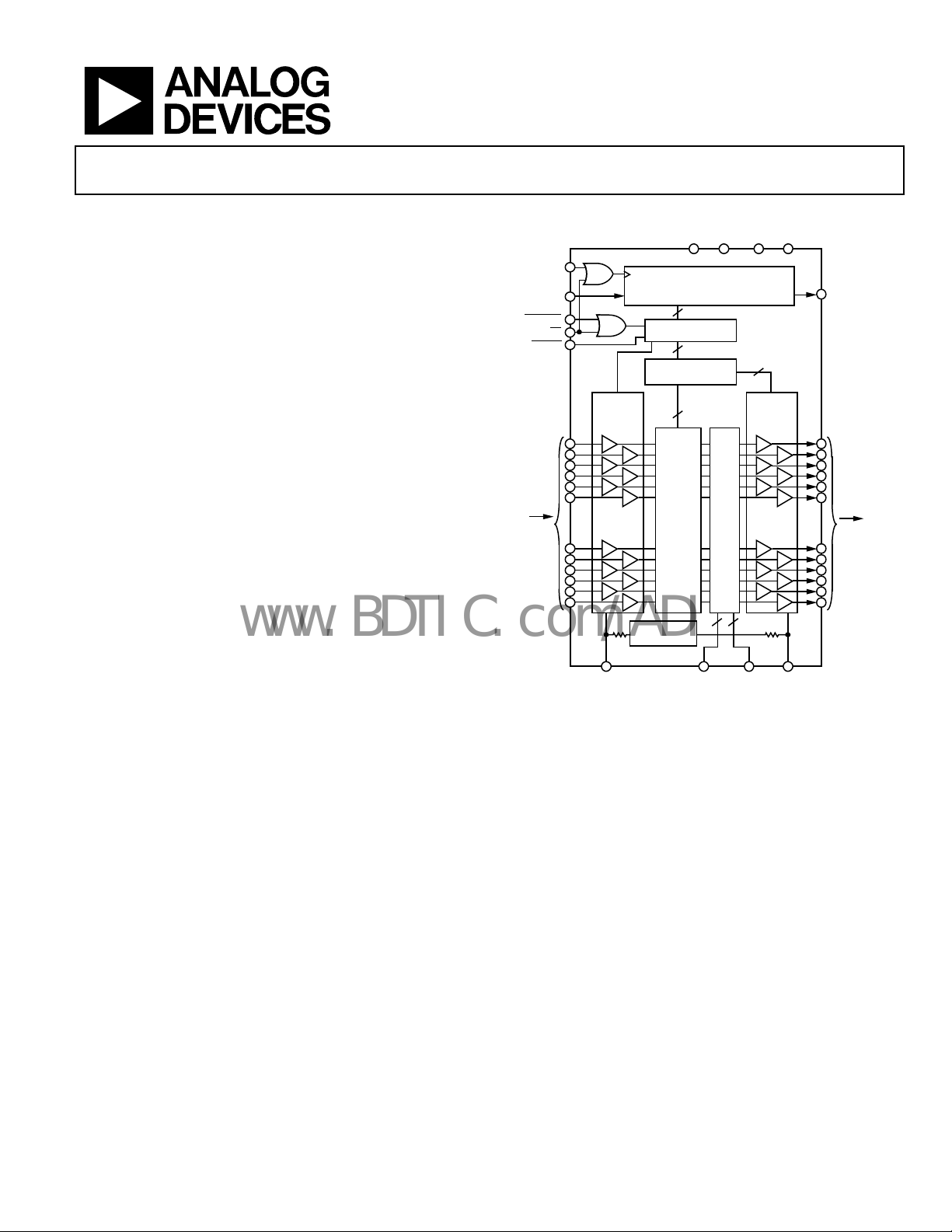
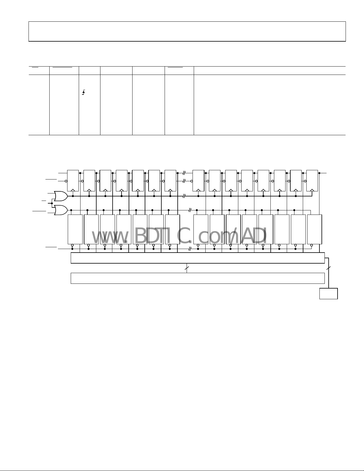
DATA IN
UPDATE
RESET
INPUTS
Analog Crosspoint Switch
ADV3200/ADV3201
FUNCTIONAL BLOCK DIAGRAM
DGNDDVCC
ADV3200
(ADV3201)
32
ENABLE/
DISABLE
OUTPUT
BUFFER
G = +1
(G = +2)
.
.
.
3232
OSD
.
.
.
CLK
CS
ENABLE/
BYPASS
SYNC-TIP
CLAMP
.
.
32
.
VCLAMP VREFOSD
193-BIT SHI FT REGISTER
PARALLEL L ATCH
32 × 5:32
DECODERS
SWITCH
.
MATRIX
.
.
REFERENCE
POS
193
192
1024
INPUTS
Figure 1.
NEG
OSD
MUX
SWITCHES
DATA
OUT
32
OUTPUTS
07176-001
GENERAL DESCRIPTION
The ADV3200/ADV3201 are 32 × 32 analog crosspoint switch
matrices. They feature a selectable sync-tip clamp input for
ac-coupled applications and an on-screen display (OSD)
insertion mux. With −48 dB of crosstalk and −80 dB isolation
at 5 MHz, the ADV3200/ADV3201 are useful in many high
density routing applications. The 0.1 dB flatness out to 60 MHz
makes the ADV3200/ADV3201 ideal for composite video
switching.
The 32 independent output buffers of the ADV3200/ADV3201
can be placed into a high impedance state for paralleling crosspoint outputs so that off channels present minimal loading to
Rev. 0
Information furnished by Analog Devices is believed to be accurate and reliable. However, no
responsibility is assumed by Analog Devices for its use, nor for any infringements of patents or other
rights of third parties that may result from its use. Specifications subject to change without notice. No
license is granted by implication or otherwise under any patent or patent rights of Analog Devices.
Trademarks and registered trademarks are the property of their respective owners.
an output bus if building a larger array. The part is available
in a gain of +1 (ADV3200) or +2 (ADV3201) for ease of use in
back-terminated load applications. A single 5 V supply, dual
±2.5 V supplies, or dual ±3.3 V supplies (G = +2) can be used
while consuming only 250 mA of idle current with all outputs
enabled. The channel switching is performed via a double
buffered, serial digital control, which can accommodate daisy
chaining of several devices.
The ADV3200/ADV3201 are packaged in a 176-lead exposed
pad LQFP (24 mm × 24 mm) and are available over the
extended industrial temperature range of −40°C to +85°C.
One Technology Way, P.O. Box 9106, Norwood, MA 02062-9106, U.S.A.
Tel: 781.329.4700 www.analog.com
Fax: 781.461.3113 ©2008 Analog Devices, Inc. All rights reserved.

ADV3200/ADV3201
www.BDTIC.com/ADI
TABLE OF CONTENTS
Features .............................................................................................. 1
Applications ....................................................................................... 1
Functional Block Diagram .............................................................. 1
General Description ......................................................................... 1
Revision History ............................................................................... 2
Specifications ..................................................................................... 3
OSD Disabled ................................................................................ 3
OSD Enabled ................................................................................. 4
Timing Characteristics (Serial Mode) ....................................... 5
Absolute Maximum Ratings ............................................................ 7
Thermal Resistance ...................................................................... 7
Power Dissipation ......................................................................... 7
ESD Caution .................................................................................. 7
Pin Configuration and Function Descriptions ............................. 8
Truth Table and Logic Diagram ............................................... 11
I/O Schematics ................................................................................ 12
Typical Performance Characteristics ........................................... 13
ADV3200 ..................................................................................... 13
ADV3201 ..................................................................................... 20
Theory of Operation ...................................................................... 27
Applications Information .............................................................. 29
Programming .............................................................................. 29
AC Coupling of Inputs .............................................................. 29
On-Screen Display (OSD) ......................................................... 31
Decoupling .................................................................................. 31
Power Dissipation....................................................................... 31
Crosstalk ...................................................................................... 32
PCB Termination Layout........................................................... 34
Outline Dimensions ....................................................................... 36
Ordering Guide .......................................................................... 36
REVISION HISTORY
10/08—Revision 0: Initial Version
Rev. 0 | Page 2 of 36

ADV3200/ADV3201
www.BDTIC.com/ADI
SPECIFICATIONS
OSD DISABLED
VS = ±2.5 V (ADV3200), VS = ±3.3 V (ADV3201) at TA = 25°C, G = +1 (ADV3200), G = +2 (ADV3201), RL = 150 Ω, all configurations,
unless otherwise noted.
Table 1.
Parameter Test Conditions/Comments Min Typ Max Unit
DYNAMIC PERFORMANCE
−3 dB Bandwidth 200 mV p-p
2 V p-p 120 MHz
Gain Flatness 0.1 dB, 200 mV p-p 60 MHz
0.1 dB, 2 V p-p 40 MHz
Settling Time 1%, 2 V step 6 ns
Slew Rate 2 V step, peak 400 V/μs
NOISE/DISTORTION PERFORMANCE
Differential Gain Error NTSC or PAL
ADV3200 0.06 %
ADV3201 0.1 %
Differential Phase Error NTSC or PAL
ADV3200 0.06 Degrees
ADV3201 0.03 Degrees
Crosstalk, All Hostile, RTI f = 5 MHz, RL = 150 Ω −48 dB
f = 5 MHz, RL = 1 kΩ −65 dB
f = 100 MHz, RL = 150 Ω −23 dB
f = 100 MHz, RL = 1 kΩ −30 dB
Off Isolation, Input-to-Output, RTI f = 5 MHz, one channel −80 dB
Input Voltage Noise 0.1 MHz to 50 MHz
ADV3200 25 nV/√Hz
ADV3201 22 nV/√Hz
DC PERFORMANCE
Gain Error
ADV3200 No load (broadcast mode) ±0.5 ±1.75 %
Broadcast mode ±0.5 ±2.2 %
ADV3201 No load (broadcast mode) ±0.5 ±2.2 %
Broadcast mode ±0.5 ±2.7 %
Gain Matching No load, channel-to-channel ±0.5 ±2.8 %
Channel-to-channel ±0.8 ±3.4 %
OUTPUT CHARACTERISTICS
Output Impedance DC, enabled 0.15 Ω
ADV3200 DC, disabled 900 1000 kΩ
ADV3201 DC, disabled 3.2 4 kΩ
Output Capacitance Disabled 3.7 pF
Output Voltage Range
ADV3200 −1.1 to +1.1 −1.2 to +1.2 V
ADV3201 −1.5 to +1.5 −1.6 to +2.0 V
No output load −1.5 to +1.5 −2.0 to +2.0 V
INPUT CHARACTERISTICS
Input Offset Voltage ±5 ±30 mV
Input Voltage Range
ADV3200 −1.1 to +1.1 −1.2 to +1.2 V
ADV3201 −0.75 to +0.75 −0.8 to +1.0 V
No output load −0.75 to +0.75 −1.0 to +1.0 V
300 MHz
Rev. 0 | Page 3 of 36

ADV3200/ADV3201
www.BDTIC.com/ADI
Parameter Test Conditions/Comments Min Typ Max Unit
Input Capacitance 3 pF
Input Resistance 1 4 MΩ
Input Bias Current
Sync-tip clamp disabled −10 −3 μA
SWITCHING CHARACTERISTICS
Enable On Time 50% update to 1% settling 50 ns
Switching Time, 2 V Step 50% update to 1% settling 40 ns
Switching Transient (Glitch) IN00 to IN31, RTI 300 mV p-p
POWER SUPPLIES
Supply Current
ADV3200 VPOS or VNEG, outputs enabled, no load 250 300 mA
VPOS or VNEG, outputs disabled 120 155 mA
ADV3201 VPOS or VNEG, outputs enabled, no load 260 310 mA
VPOS or VNEG, outputs disabled 130 165 mA
DVCC 2.5 3.5 mA
Supply Voltage Range VPOS − VNEG
PSR VNEG, VPOS, f = 1 MHz
ADV3200 −50 dB
ADV3201 −45 dB
OPERATING TEMPERATURE RANGE
Temperature Range Operating (still air) −40 to +85 °C
θJA Operating (still air) 16 °C/W
Sync-tip clamp enabled,
= VCLAMP + 0.1 V
V
IN
Sync-tip clamp enabled,
VIN = VCLAMP − 0.1 V
0.1 3 12 μA
−2.9 −1 −0.25 mA
5 ± 10% to
6.6 ± 10%
V
OSD ENABLED
VS = ±2.5 V (ADV3200), VS = ±3.3 V (ADV3201) at TA = 25°C, G = +1 (ADV3200), G = +2 (ADV3201), RL = 150 Ω, all configurations,
unless otherwise noted.
Table 2.
Parameter Test Conditions/Comments Min Typ Max Unit
OSD DYNAMIC PERFORMANCE
−3 dB Bandwidth
ADV3200 200 mV p-p
2 V p-p 135 MHz
ADV3201 200 mV p-p
2 V p-p 130 MHz
Gain Flatness 0.1 dB, 200 mV p-p 35 MHz
0.1 dB, 2 V p-p 35 MHz
Settling Time 1%, 2 V step 6 ns
Slew Rate 2 V step, peak 400 V/μs
OSD NOISE/DISTORTION PERFORMANCE
Differential Gain Error NTSC or PAL
ADV3200 0.12 %
ADV3201 0.35 %
Differential Phase Error NTSC or PAL
ADV3200 0.06 Degrees
ADV3201 0.04 Degrees
Input Voltage Noise 0.5 MHz to 50 MHz
ADV3200 27 nV/√Hz
ADV3201 25 nV/√Hz
170 MHz
150 MHz
Rev. 0 | Page 4 of 36
ADV3200/ADV3201
www.BDTIC.com/ADI
Parameter Test Conditions/Comments Min Typ Max Unit
OSD DC PERFORMANCE
Gain Error
ADV3200 No load ±0.1 ±2.3 %
±0.1 ±2.7 %
ADV3201 No load ±0.1 ±2.2 %
±0.1 ±2.7 %
OSD INPUT CHARACTERISTICS
Input Offset Voltage ±5 ±30 mV
Input Bias Current −10 −4 μA
OSD SWITCHING CHARACTERISTICS
OSD Switch Delay, 2 V Step 50% OSD switch to 1% settling 20 ns
OSD Switching Transient (Glitch)
ADV3200 15 mV p-p
ADV3201 40 mV p-p
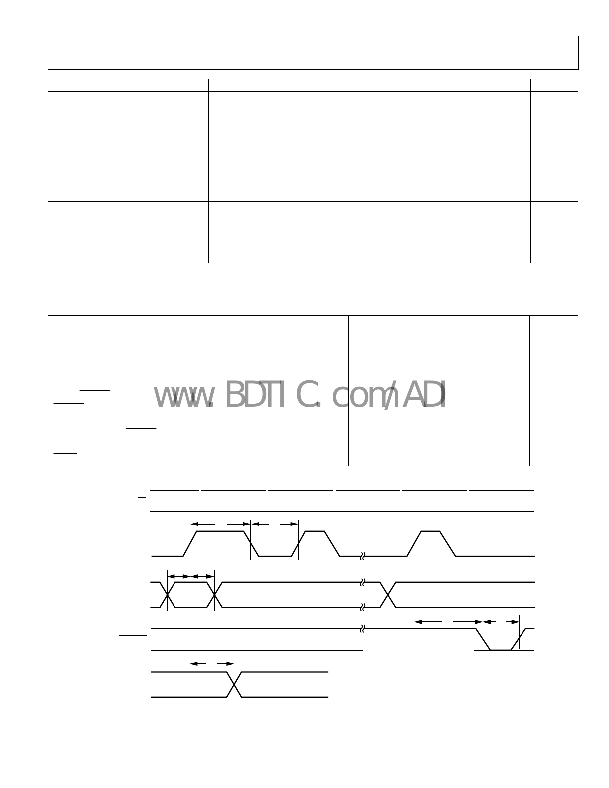
TIMING CHARACTERISTICS (SERIAL MODE)
Table 3.
Limit
Parameter Symbol Min Typ Max Unit
Serial Data Setup Time t1 40 ns
CLK Pulse Width t2 50 ns
Serial Data Hold Time t3 50 ns
CLK Pulse Separation t4 150 ns
t
CLK to UPDATE Delay
UPDATE Pulse Width
CLK to DATA OUT Valid t7 130 ns
Propagation Delay, UPDATE to Switch On or Off
Data Load Time, CLK = 5 MHz, Serial Mode 38.6 μs
RESET Time
50 160 ns
5
t
40 ns
6
50 ns
160 ns
CS
CLK
DATA IN
1 = LATCHED
UPDATE
0 = TRANSPARENT
DATA OUT
1
0
t
1
0
t
1t3
1
0
CLAMP
ON/OFF
2
t
7
t
4
Figure 2. Timing Diagram, Serial Mode
Rev. 0 | Page 5 of 36
LOAD DATA INTO
SERIAL REGISTER
ON RISING EDGE
TRANSFER DATA FROM SERIAL
LATCHES DURING LOW LEVEL
OUT00 (D0)OUT31 (D5)
t
5
REGISTER TO PARALLEL
t
6
07176-002
ADV3200/ADV3201
www.BDTIC.com/ADI
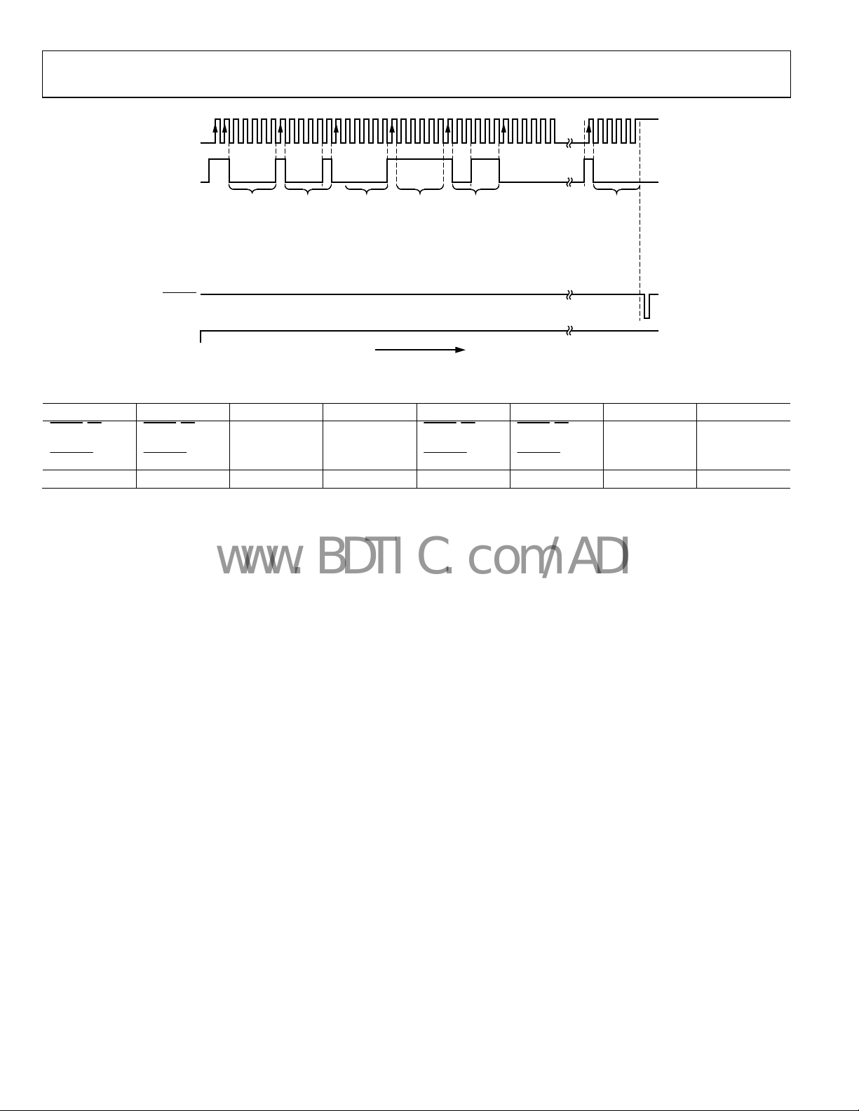
DATA IN
UPDATE
0 1 2 3 4 5 6 7 8 9 10 11 1213 19 25 31 36
CLK
T = 0
IN00
CONNECT TO
ENABLE OUT31
ENABLE SYNC-TIP CLAMP
IN01
CONNECT TO
ENABLE OUT30
DON’T CARE
DISABLE O UT29
INCREASING TIME
IN31
CONNECT TO
ENABLE OUT28
ENABLE OUT27
187 192
IN07
CONNECT TO
IN00
CONNECT TO
ENABLE OUT00
07176-105
Figure 3. Programming Example
Table 4. Logic Levels, DVCC = 3.3 V
VIH VIL V
RESET, CS,
CLK, DATA IN,
UPDATE
, OSDS
RESET
, CS,
CLK, DATA IN,
UPDATE
, OSDS
V
OH
I
OL
DATA OUT DATA OUT
I
IH
, CS,
RESET
CLK, DATA IN,
UPDATE
, OSDS
I
IL
RESET
, CS,
CLK, DATA IN,
UPDATE
, OSDS
I
OH
OL
DATA OUT DATA OUT
2.5 V min 0.8 V max 2.7 V min 0.5 V max 0.5 μA typ −0.5 μA typ 3 mA typ −3 mA typ
Rev. 0 | Page 6 of 36

ADV3200/ADV3201
www.BDTIC.com/ADI
ABSOLUTE MAXIMUM RATINGS
Table 5.
Parameter Rating
Analog Supply Voltage
(VPOS − VNEG)
Digital Supply Voltage
(DVCC − DGND)
Ground Potential Difference
(VNEG − DGND)
Maximum Potential Difference
DVCC − VNEG 9.4 V
Disabled Outputs
ADV3200 (|V
ADV3201
(|V
OSD
|VCLAMP − V
VREF Input Voltage
ADV3200 VPOS − 3.5 V to VNEG + 3.5 V
ADV3201 VPOS − 4 V to VNEG + 4 V
Analog Input Voltage VNEG to VPOS
Digital Input Voltage DVCC
Output Voltage
(Disabled Analog Output)
Output Short-Circuit Duration Momentary
Output Short-Circuit Current 45 mA
Storage Temperature Range −65°C to +125°C
Operating Temperature Range −40°C to +85°C
Lead Temperature
(Soldering 10 sec)
Junction Temperature 150°C
− V
OSD
− (V
OUT
| 6 V
INxx
|) <3 V
OUT
+ VREF)/2|)
7.5 V
6 V
+0.5 V to −4 V
<3 V
(VPOS − 1 V) to (VNEG + 1 V)
300°C
POWER DISSIPATION
The ADV3200/ADV3201 are operated with ±2.5 V, 5 V, or
±3.3 V supplies and can drive loads down to 150 , resulting in
a large range of possible power dissipations. For this reason,
extra care must be taken to derate the operating conditions
based on ambient temperature.
The ADV3200/ADV3201 are packaged in a 176-lead exposed
pad LQFP. The junction-to-ambient thermal impedance (θ
the ADV3200/ADV3201 is 16°C/W. For long-term reliability,
the maximum allowed junction temperature of the die should
not exceed 150°C. Temporarily exceeding this limit may cause a
shift in parametric performance due to a change in stresses
exerted on the die by the package. Exceeding a junction
temperature of 175°C for an extended period can result in
device failure. Figure 4 shows the range of allowed internal die
power dissipations that meet these conditions over the −40°C to
+85°C ambient temperature range. When using Figure 4, do not
include external load power in the maximum power calculation,
but do include load current dropped on the die output
transistors.
9
TJ = 150°C
8
7
6
JA
) of
Stresses above those listed under Absolute Maximum Ratings
may cause permanent damage to the device. This is a stress
rating only; functional operation of the device at these or any
other conditions above those indicated in the operational
section of this specification is not implied. Exposure to absolute
maximum rating conditions for extended periods may affect
device reliability.
THERMAL RESISTANCE
θJA is specified for the worst-case conditions, that is, a device
soldered in a circuit board for surface-mount packages.
Table 6. Thermal Resistance
Package Type θJA Unit
176-Lead LQFP_EP 16 °C/W
Rev. 0 | Page 7 of 36
5
MAXIMUM POWER (W)
4
3
15 25 35 45 55 65 75 85
AMBIENT TEMPERATURE (°C)
Figure 4. Maximum Die Power Dissipation vs. Ambient Temperature
ESD CAUTION
07176-003
ADV3200/ADV3201
www.BDTIC.com/ADI
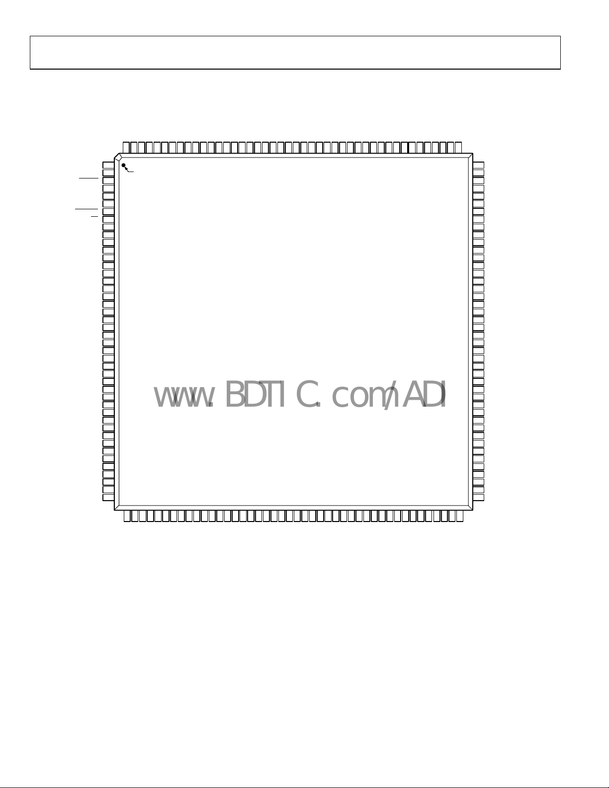
PIN CONFIGURATION AND FUNCTION DESCRIPTIONS
OSD10
OSD09
OSD08
VPOS
OUT15
VNEG
OUT14
VPOS
OUT13
VNEG
OUT12
VPOS
OUT11
VNEG
OUT10
VPOS
OUT09
VNEG
OUT08
VPOS
OUT07
VNEG
OUT06
VPOS
OUT05
VNEG
OUT04
VPOS
OUT03
VNEG
OUT02
VPOS
OUT01
VNEG
OUT00
VPOS
OSD07
OSD06
OSD05
OSD04
OSD03
OSD02
OSD01
DGND
148
150
151
152
153
155
156
157
158
159
160
161
ADV3200/ADV3201
TOP VIEW
(Not to Scale)
154
149
146
139
136
135
132
VNEG
131
OSD11
130
OSD12
129
OSD13
128
OSD14
127
OSD15
126
OSDS16
125
IN16
124
OSDS17
123
IN17
122
OSDS18
121
IN18
120
OSDS19
119
IN19
118
OSDS20
117
IN20
116
OSDS21
115
IN21
114
OSDS22
113
IN22
112
OSDS23
111
IN23
110
OSDS24
109
IN24
108
OSDS25
107
IN25
106
OSDS26
105
IN26
104
OSDS27
103
IN27
102
OSDS28
101
IN28
100
OSDS29
99
IN29
98
OSDS30
97
IN30
96
OSDS31
95
IN31
94
VPOS
93
OSD16
92
OSD17
91
OSD18
90
OSD19
89
VNEG
133
134
137
138
140
141
142
143
144
145
147
DVCC
OSD00
RESET
CLK
DATA IN
DATA OUT
UPDATE
OSDS15
IN00
OSDS14
IN01
OSDS13
IN02
OSDS12
IN03
OSDS11
IN04
OSDS10
IN05
OSDS09
IN06
OSDS08
IN07
OSDS07
IN08
OSDS06
IN09
OSDS05
IN10
OSDS04
IN11
OSDS03
IN12
OSDS02
IN13
OSDS01
IN14
OSDS00
IN15
VNEG
VREF
VCLAMP
OSD31
CS
172
171
170
169
166
167
165
164
163
162
173
176
174
175
1
PIN 1
2
3
4
5
6
7
8
9
10
11
12
13
14
15
16
17
18
19
20
21
22
23
24
25
26
27
28
29
30
31
32
33
34
35
36
37
38
39
40
41
42
43
44
168
45
OSD3046OSD2947OSD2848OSD2749OSD2650OSD2551OSD24
NOTES
1. OSDSxx: OS D SELECT F OR OUTxx
OSDxx: OSD VIDEO INPUT FOR OUTxx
2. THE EXPOSED PAD SHOULD BE
CONNECTED TO ANALOG GRO UND.
52
53
54
55
56
57
58
59
60
61
62
63
64
65
66
VPOS
VPOS
VNEG
OUT31
OUT30
VPOS
VNEG
OUT29
OUT28
VPOS
VNEG
OUT27
VNEG
OUT26
OUT25
Figure 5. Pin Configuration
Rev. 0 | Page 8 of 36
67
68
69
70
71
72
73
74
75
76
77
78
79
80
81
82
83
84
85
VPOS
OUT24
VPOS
VNEG
OUT23
OUT22
VPOS
VNEG
OUT21
OUT20
VPOS
VNEG
OUT19
OUT18
VPOS
VNEG
OUT17
OUT16
OSD2386OSD2287OSD2188OSD20
07176-004
ADV3200/ADV3201
www.BDTIC.com/ADI
Table 7. Pin Function Descriptions
Pin Mnemonic Description
1 DVCC Digital Positive Power Supply.
2 OSD00 OSD Input Number 0.
3
4 CLK Control Pin: Serial Data Clock.
5 DATA IN Control Pin: Serial Data In.
6 DATA OUT Control Pin: Serial Data Out.
7
8
9 OSDS15 Control Pin: OSD Select Number 15.
10 IN00 Input Number 0.
11 OSDS14 Control Pin: OSD Select Number 14.
12 IN01 Input Number 1.
13 OSDS13 Control Pin: OSD Select Number 13.
14 IN02 Input Number 2.
15 OSDS12 Control Pin: OSD Select Number 12.
16 IN03 Input Number 3.
17 OSDS11 Control Pin: OSD Select Number 11.
18 IN04 Input Number 4.
19 OSDS10 Control Pin: OSD Select Number 10.
20 IN05 Input Number 5.
21 OSDS09 Control Pin: OSD Select Number 9.
22 IN06 Input Number 6.
23 OSDS08 Control Pin: OSD Select Number 8.
24 IN07 Input Number 7.
25 OSDS07 Control Pin: OSD Select Number 7.
26 IN08 Input Number 8.
27 OSDS06 Control Pin: OSD Select Number 6.
28 IN09 Input Number 9.
29 OSDS05 Control Pin: OSD Select Number 5.
30 IN10 Input Number 10.
31 OSDS04 Control Pin: OSD Select Number 4.
32 IN11 Input Number 11.
33 OSDS03 Control Pin: OSD Select Number 3.
34 IN12 Input Number 12.
35 OSDS02 Control Pin: OSD Select Number 2.
36 IN13 Input Number 13.
37 OSDS01 Control Pin: OSD Select Number 1.
38 IN14 Input Number 14.
39 OSDS00 Control Pin: OSD Select Number 0.
40 IN15 Input Number 15.
41 VNEG Analog Negative Power Supply.
42 VREF
43 VCLAMP
44 OSD31 OSD Input Number 31.
45 OSD30 OSD Input Number 30.
46 OSD29 OSD Input Number 29.
47 OSD28 OSD Input Number 28.
48 OSD27 OSD Input Number 27.
49 OSD26 OSD Input Number 26.
RESET
UPDATE
CS
Control Pin: First and Second Rank Reset.
Control Pin: Second Rank Write Strobe.
Control Pin: Chip Select.
Reference Voltage. See the Theory of
Operation section for details.
Sync-Tip Clamp Voltage. See the
Theory of Operation section for details.
Pin Mnemonic Description
50 OSD25 OSD Input Number 25.
51 OSD24 OSD Input Number 24.
52 VPOS Analog Positive Power Supply.
53 OUT31 Output Number 31.
54 VNEG Analog Negative Power Supply.
55 OUT30 Output Number 30.
56 VPOS Analog Positive Power Supply.
57 OUT29 Output Number 29.
58 VNEG Analog Negative Power Supply.
59 OUT28 Output Number 28.
60 VPOS Analog Positive Power Supply.
61 OUT27 Output Number 27.
62 VNEG Analog Negative Power Supply.
63 OUT26 Output Number 26.
64 VPOS Analog Positive Power Supply.
65 OUT25 Output Number 25.
66 VNEG Analog Negative Power Supply.
67 OUT24 Output Number 24.
68 VPOS Analog Positive Power Supply.
69 OUT23 Output Number 23.
70 VNEG Analog Negative Power Supply.
71 OUT22 Output Number 22.
72 VPOS Analog Positive Power Supply.
73 OUT21 Output Number 21.
74 VNEG Analog Negative Power Supply.
75 OUT20 Output Number 20.
76 VPOS Analog Positive Power Supply.
77 OUT19 Output Number 19.
78 VNEG Analog Negative Power Supply.
79 OUT18 Output Number 18.
80 VPOS Analog Positive Power Supply.
81 OUT17 Output Number 17.
82 VNEG Analog Negative Power Supply.
83 OUT16 Output Number 16.
84 VPOS Analog Positive Power Supply.
85 OSD23 OSD Input Number 23.
86 OSD22 OSD Input Number 22.
87 OSD21 OSD Input Number 21.
88 OSD20 OSD Input Number 20.
89 VNEG Analog Negative Power Supply.
90 OSD19 OSD Input Number 19.
91 OSD18 OSD Input Number 18.
92 OSD17 OSD Input Number 17.
93 OSD16 OSD Input Number 16.
94 VPOS Analog Positive Power Supply.
95 IN31 Input Number 31.
96 OSDS31 Control Pin: OSD Select Number 31.
97 IN30 Input Number 30.
98 OSDS30 Control Pin: OSD Select Number 30.
99 IN29 Input Number 29.
100 OSDS29 Control Pin: OSD Select Number 29.
Rev. 0 | Page 9 of 36
ADV3200/ADV3201
www.BDTIC.com/ADI
Pin Mnemonic Description
101 IN28 Input Number 28.
102 OSDS28 Control Pin: OSD Select Number 28.
103 IN27 Input Number 27.
104 OSDS27 Control Pin: OSD Select Number 27.
105 IN26 Input Number 26.
106 OSDS26 Control Pin: OSD Select Number 26.
107 IN25 Input Number 25.
108 OSDS25 Control Pin: OSD Select Number 25.
109 IN24 Input Number 24.
110 OSDS24 Control Pin: OSD Select Number 24.
111 IN23 Input Number 23.
112 OSDS23 Control Pin: OSD Select Number 23.
113 IN22 Input Number 22.
114 OSDS22 Control Pin: OSD Select Number 22.
115 IN21 Input Number 21.
116 OSDS21 Control Pin: OSD Select Number 21.
117 IN20 Input Number 20.
118 OSDS20 Control Pin: OSD Select Number 20.
119 IN19 Input Number 19.
120 OSDS19 Control Pin: OSD Select Number 19.
121 IN18 Input Number 18.
122 OSDS18 Control Pin: OSD Select Number 18.
123 IN17 Input Number 17.
124 OSDS17 Control Pin: OSD Select Number 17.
125 IN16 Input Number 16.
126 OSDS16 Control Pin: OSD Select Number 16.
127 OSD15 OSD Input Number 15.
128 OSD14 OSD Input Number 14.
129 OSD13 OSD Input Number 13.
130 OSD12 OSD Input Number 12.
131 OSD11 OSD Input Number 11.
132 VNEG Analog Negative Power Supply.
133 OSD10 OSD Input Number 10.
134 OSD09 OSD Input Number 9.
135 OSD08 OSD Input Number 8.
136 VPOS Analog Positive Power Supply.
137 OUT15 Output Number 15.
138 VNEG Analog Negative Power Supply.
139 OUT14 Output Number 14.
Pin Mnemonic Description
140 VPOS Analog Positive Power Supply.
141 OUT13 Output Number 13.
142 VNEG Analog Negative Power Supply.
143 OUT12 Output Number 12.
144 VPOS Analog Positive Power Supply.
145 OUT11 Output Number 11.
146 VNEG Analog Negative Power Supply.
147 OUT10 Output Number 10.
148 VPOS Analog Positive Power Supply.
149 OUT09 Output Number 9.
150 VNEG Analog Negative Power Supply.
151 OUT08 Output Number 8.
152 VPOS Analog Positive Power Supply.
153 OUT07 Output Number 7.
154 VNEG Analog Negative Power Supply.
155 OUT06 Output Number 6.
156 VPOS Analog Positive Power Supply.
157 OUT05 Output Number 5.
158 VNEG Analog Negative Power Supply.
159 OUT04 Output Number 4.
160 VPOS Analog Positive Power Supply.
161 OUT03 Output Number 3.
162 VNEG Analog Negative Power Supply.
163 OUT02 Output Number 2.
164 VPOS Analog Positive Power Supply.
165 OUT01 Output Number 1.
166 VNEG Analog Negative Power Supply.
167 OUT00 Output Number 0.
168 VPOS Analog Positive Power Supply.
169 OSD07 OSD Input Number 7.
170 OSD06 OSD Input Number 6.
171 OSD05 OSD Input Number 5.
172 OSD04 OSD Input Number 4.
173 OSD03 OSD Input Number 3.
174 OSD02 OSD Input Number 2.
175 OSD01 OSD Input Number 1.
176 DGND Digital Negative Power Supply.
Exposed Pad Connect to analog ground.
Rev. 0 | Page 10 of 36
ADV3200/ADV3201
www.BDTIC.com/ADI
TRUTH TABLE AND LOGIC DIAGRAM
Table 8. Operation Truth Table
CS
X
UPDATE
1
X X X X 0
0 1
0 0 X X X 1
1 X X X X 1 Chip is not selected. No change in logic.
1
X = don’t care.
2
Datai: serial data.
DATA
IN
R
ESET
CLK
CS
CLK DATA IN DATA OUT
RESET
Operation/Comment
Asynchronous reset. All outputs are disabled. The 193-bit shift
register is reset to all 0s.
2
Data
i
Data
i-193
1
The data on the serial DATA IN line is loaded into the serial
register. The first bit clocked into the serial register appears at
DATA OUT 193 clock cycles later.
Switch matrix update. Data in the 193-bit shift register is transferred into the parallel latches that control the switch array and
sync-tip clamps.
D
Q
DQ
DQ
DQ
DQ
DQ
DQ
CLR CLR CLR CL R CLR CLR CLR CLR CL R CLR CL R CLR CL R CLR
CLR
CLK
CLK
CLK
CLK
CLK
CLK
CLK
. . .
DQ
CLK
DQ
CLK
DQ
CLK
DQ
CLK
DQ
CLK
DQ
CLK
DQ
CLK
DQ
CLK
DATA
OUT
UPDATE
RESET
LE D
OUT00
0
LSB
192
CLR Q
LE D
OUT00
1
LSB
191
CLR Q
LE D
OUT00
2
LSB
190
CLR Q
LE D
OUT00
3
LSB
189
CLR Q
LE D
OUT00
4
LSB
188
CLR Q
LE D
LE D
OUT00
OUT01
EN
187
0
LSB
186
CLR Q
SWITCH MATRIX
MSB
CLR Q
Figure 6. Logic Diagram
LE D
LE D
LE D
LE D
LE D
OUT30
OUT31
OUT31
EN
. . .
MSB
CLR Q
DECODE
1024 32
0
LSB
7
6
CLR Q
1
LSB
5
CLR Q
OUT31
2
LSB
4
CLR Q
OUT31
3
LSB
3
CLR Q
LE D
OUT31
4
LSB
2
CLR Q
LE D
OUT31
EN
MSB
1
CLR Q
LE D
OUT31
SYNC
CLR Q
TIP
EN
0
OUTPUT
ENABLE
07176-053
Rev. 0 | Page 11 of 36

ADV3200/ADV3201
www.BDTIC.com/ADI
I/O SCHEMATICS
4kΩ
(ADV3201 ONLY)
VREF
Figure 7. Enabled Output
(See Also Figure 16)
OUT
4kΩ
3.7pF
(ADV3201 ONLY)
VREF
Figure 8. Disabled Output
(See Also Figure 16)
IN
VNEG
Figure 9. Receiver
(See Also Figure 16)
OUT
CLK, UPDATE,
DATA IN,
OSDS, CS
07176-054
(CS ONLY)
25kΩ
DGND
1kΩ
DGND
07176-059
Figure 12. Logic Input
(See Also Figure 16)
DVCC
DATA OUT
07176-055
DGND
07176-060
Figure 13. Logic Output
(See Also Figure 16)
VREF
VNEG
6kΩ
50µA
07176-061
VCLAMP
07176-056
Figure 14. VCLAMP Input
(See Also Figure 16)
IN
5µA
VNEG
07176-058
Figure 10. Receiver with Sync-Tip Clamp Enabled
(See Also Figure 16)
DVCC
25kΩ
RESET
1kΩ
DGND
07176-057
Figure 11. Reset Input
VREF, VCLAMP,
OSD, IN, OUT
VPOS
2.5kΩ
VR
EF
(5kΩ FOR ADV3201)
2.5kΩ
(5kΩ FOR ADV3201)
VNEG
Figure 15. VREF Input
(See Also Figure 16)
VPOS
VNEG
Figure 16. ESD Protection Map
VPOS
DVCC
DGND
07176-062
CLK, RESET,
UPDATE, CS,
DATA IN,
DATA OUT,
OSDS
07176-063
(See Also Figure 16)
Rev. 0 | Page 12 of 36

ADV3200/ADV3201
www.BDTIC.com/ADI
TYPICAL PERFORMANCE CHARACTERISTICS
ADV3200
VS = ±2.5 V at TA = 25°C, RL = 150 .
2
0
–2
–4
–6
GAIN (dB)
–8
–10
INxx
OSDxx
2
1
0
–1
GAIN (dB)
–2
–3
10pF
0pF
5pF
2pF
–12
1 10 100 1k
FREQUENCY (MHz )
Figure 17. ADV3200 Small Signal Frequency Response, 200 mV p-p
2
0
–2
–4
–6
GAIN (dB)
–8
–10
–12
1 10 100 1k
FREQUENCY (MHz )
OSDxx
INxx
Figure 18. ADV3200 Large Signal Frequency Response, 2 V p-p
4
2
0
–2
–4
GAIN (dB)
–6
–8
10pF
5pF
2pF
0pF
–4
1 10 100 1k
07176-005
FREQUENCY (MHz )
07176-012
Figure 20. ADV3200 Large Signal Frequency Response with Capacitive Loads,
2 V p-p
4
2
10pF
0pF
5pF
2pF
07176-011
0
–2
–4
GAIN (dB)
–6
–8
–10
1 10 100 1k
07176-009
FREQUENCY (MHz )
Figure 21. ADV3200 OSD Small Signal Frequency Response
with Capacitive Loads, 200 mV p-p
2
1
5pF
0
–1
GAIN (dB)
–2
–3
10pF
0pF
2pF
–10
1 10 100 1k
FREQUENCY (MHz )
07176-010
Figure 19. ADV3200 Small Signal Frequency Response with Capacitive Loads,
200 mV p-p
Rev. 0 | Page 13 of 36
–4
1 10 100 1k
FREQUENCY (MHz )
07176-013
Figure 22. ADV3200 OSD Large Signal Frequency Response with Capacitive
Loads, 2 V p-p

ADV3200/ADV3201
www.BDTIC.com/ADI
600
90
500
400
300
COUNT
200
100
0
354 362 370 378 386 394
FREQUENCY (MHz )
Figure 23. ADV3200 −3 dB Bandwidth Histogram, One Device,
All 1024 Channels
500
475
450
425
400
375
–3dB BANDWIDTH ( MHz)
350
325
300
123456789
1011121314151617181920212223242526272829303132
NUMBER OF ENABLED CHANNELS
Figure 24. ADV3200 Small Signal Bandwidth vs. Enabled Channels
80
70
60
50
40
NOISE (nV/ Hz)
30
20
10
0
0.001 0.01 0.1 1 10
07176-083
FREQUENCY (MHz)
07176-079
Figure 26. ADV3200 Output Noise
140
120
100
80
60
NOISE (nV/ Hz)
40
20
0
07176-015
0.001 0.01 0.1 1 10
FREQUENCY (MHz)
07176-085
Figure 27. ADV3200 OSD Output Noise
0
–10
–20
–30
–40
PSR (dB)
–50
–60
–70
–80
0.1 1 10 100
FREQUENCY (MHz)
VNEG
VPOS
Figure 25. ADV3200 Power Supply Rejection
07176-064
Rev. 0 | Page 14 of 36
0
–10
–20
–30
–40
–50
–60
CROSSTALK (d B)
–70
–80
–90
–100
1 10 100 1k
FREQUENCY (MHz )
Figure 28. ADV3200 Crosstalk, One Adjacent Channel, RTO
07176-018

ADV3200/ADV3201
www.BDTIC.com/ADI
0
–10
–20
–30
–40
–50
–60
CROSSTALK (d B)
–70
–80
–90
–100
1 10 100 1k
FREQUENCY (MHz )
Figure 29. ADV3200 Crosstalk, All Hostile, RTO
07176-017
1M
100k
10k
1k
IMPEDANCE (Ω)
100
10
1
0.1 1 10 100 1k
FREQUENCY (MHz)
Figure 32. ADV3200 Output Impedance, Disabled
07176-021
0
–10
–20
–30
–40
–50
–60
FEEDTHROUG H (dB)
–70
–80
–90
–100
1M 10M 100M 1G
FREQUENCY (Hz)
Figure 30. ADV3200 Off Isolation, RTO
1M
100k
10k
1k
IMPEDANCE (Ω)
100
10
1
0.1 1 10 100 1k
FREQUENCY (MHz)
Figure 31. ADV3200 Input Impedance
100
10
IMPEDANCE (Ω)
1
0.1
07176-019
2 10 100 1k
FREQUENCY (MHz)
07176-080
Figure 33. ADV3200 Output Impedance, Enabled
0.12
0.08
0.04
(V)
0
OUT
V
–0.04
OSDxx
–0.08
–0.12
0 2 4 6 8 101214 161820
07176-020
TIME (ns)
INxx
07176-023
Figure 34. ADV3200 Small Signal Pulse Response, 200 mV p-p
Rev. 0 | Page 15 of 36

ADV3200/ADV3201
www.BDTIC.com/ADI
1.2
600
0.8
0.4
(V)
0
OUT
V
–0.4
INxx
–0.8
–1.2
0 2 4 6 8 101214 161820
TIME (ns)
OSDxx
Figure 35. ADV3200 Large Signal Pulse Response, 2 V p-p
2
UPDATE
V
RISING EDGE
1
(V)
0
OUT
V
–1
OUT
V
FALL I NG E DG E
OUT
3.5
2.5
1.5
0.5
400
200
0
dV/dT (V/µs)
–200
–400
–600
024 68101214161820
07176-024
TIME (ns)
RISING EDG E
FALLING EDGE
07176-025
Figure 38. ADV3200 Slew Rate
0.1
0
(V)
–0.1
OUT
UPDATE (V)
V
–0.2
–2
0 20 40 60 80 100
TIME (ns)
Figure 36. ADV3200 Switching Time
2
OSDS
V
RISING EDG E
1
(V)
0
OUT
V
–1
–2
0 20 40 60 80 100
TIME (ns)
OUT
V
FALLING EDGE
OUT
Figure 37. ADV3200 OSD Switching Time
–0.5
3
2
1
0
–1
–0.3
0 20 40 60 80 100
07176-065
TIME (ns)
07176-067
Figure 39. ADV3200 Switching Glitch
15
10
(mV)
5
OSDS (V)
07176-066
OUT
V
0
–5
0 20 40 60 80 100
TIME (ns)
07176-068
Figure 40. ADV3200 OSD Switching Glitch
Rev. 0 | Page 16 of 36

ADV3200/ADV3201
www.BDTIC.com/ADI
0.05
0.04
0.03
0.02
0.01
0
–0.01
–0.02
DIFFE RENTI AL GAI N (%)
–0.03
–0.04
–0.05
–0.7 –0.5 –0.3 –0.1 0.1 0.3 0.5 0.7
INPUT DC OFFSET (V)
Figure 41. ADV3200 Differential Gain, Carrier Frequency = 3.58 MHz,
Subcarrier Amplitude = 300 mV p-p
07176-087
0.04
0.02
0
–0.02
–0.04
–0.06
DIFFERENT IAL PHASE (Degrees)
–0.08
–0.10
–0.7 –0. 5 –0.3 –0.1 0.1 0.3 0.5 0.7
INPUT DC OFFSET (V)
07176-090
Figure 44. ADV3200 OSD Differential Phase, Carrier Frequency = 3.58 MHz,
Subcarrier Amplitude = 300 mV p-p
0.010
0.005
0
–0.005
–0.010
DIFFERENTIAL PHASE (Degrees)
–0.015
–0.020
–0.7 –0.5 –0.3 –0.1 0.1 0.3 0.5 0.7
INPUT DC OFFSET (V)
Figure 42. ADV3200 Differential Phase, Carrier Frequency = 3.58 MHz,
Subcarrier Amplitude = 300 mV p-p
0.05
0.03
0.01
–0.01
–0.03
–0.05
–0.07
–0.09
DIFFERENTIAL GAIN (%)
–0.11
–0.13
–0.15
–0.7 –0. 5 –0.3 –0.1 0.1 0.3 0.5 0.7
INPUT DC OFFSET (V)
07176-089
Figure 43. ADV3200 OSD Differential Gain, Carrier Frequency = 3.58 MHz,
Subcarrier Amplitude = 300 mV p-p
280
I
, I
(BROADCAST)
POS
260
240
220
200
(mA)
NEG
, I
180
POS
I
160
140
120
100
–50 –30 –10 10 30 50 70 90
07176-088
I
POS
NEG
, I
(ALL OUT PUTS DISABLE D)
NEG
TEMPERATURE (° C)
07176-098
Figure 45. ADV3200 Supply Current vs. Temperature
300
275
250
225
(mA)
200
NEG
, I
175
POS
I
150
125
100
0 2 4 6 8 1012141618 20222426283032
NUMBER OF ENABLED O UTPUTS
07176-026
Figure 46. ADV3200 Supply Current vs. Enabled Outputs
Rev. 0 | Page 17 of 36

ADV3200/ADV3201
www.BDTIC.com/ADI
250
200
150
COUNT
100
50
0
–20
–18
–16
–14
–12
–8–6–4
–10
02468
–2
OFFSET (mV)
1012141618
20
07176-092
Figure 47. ADV3200 Input Offset Distribution, One Device, All 1024 Channels
180
160
140
120
100
80
COUNT
60
40
20
0
–1.5
–1.4
–1.3
–1.2
–1.1
–1.0
–0.9
–0.8
–0.7
–0.6
–0.5
GAIN ERROR (%)
0
0.1
0.2
0.3
0.4
0.5
0.6
0.7
0.8
0.9
–0.4
–0.3
–0.2
–0.1
1.0
07176-100
Figure 50. ADV3200 Gain Error Distribution, One Device, All 1024 Channels
1.5
UPDATE
1.0
0.5
(V)
0
OUT
V
–0.5
–1.0
–1.5
0 20 40 60 80 100
TIME (ns)
V
RISING EDG E
OUT
V
FALLING EDGE
OUT
Figure 48. ADV3200 Enable Time
70
(V
- VIN)/V
OUT
60
50
40
30
OUTPUT ERROR (%)
20
10
IN
V
IN
V
OUT
1.4
1.0
0.6
0.2
–0.2
–0.6
–1.0
4
3
2
1
UPDATE (V)
0
–1
–2
07176-069
0.15
0.10
0.05
(V)
0
OUT
V
–0.05
–0.10
–0.15
0 2 4 6 8 101214 161820
2pF
0pF
10pF
5pF
TIME (ns)
07176-027
Figure 51. ADV3200 Small Signal Pulse with Capacitive Loads, 200 mV p-p
0.15
0.10
0.05
2pF
(V)
OUT
V
(V)
OUT
V
0
–0.05
–0.10
10pF
0pF
5pF
0
–5 0 5 10 15
TIME (ns)
–1.4
07176-070
Figure 49. ADV3200 Settling Time
Rev. 0 | Page 18 of 36
–0.15
0 2 4 6 8 101214 161820
TIME (ns)
Figure 52. ADV3200 OSD Small Signal Pulse with Capacitive Loads,
200 mV p-p
07176-028

ADV3200/ADV3201
www.BDTIC.com/ADI
1.5
1.0
0.5
(V)
0
OUT
V
–0.5
–1.0
10pF
2pF
5pF
0pF
2
1
0
VOLTAGE (V)
–1
VIN = ±1.65V
VIN = ±1.45V
V
@ VIN = ±1.65V
OUT
V
@ VIN = ±1.45V
OUT
–1.5
0 2 4 6 8 101214 161820
TIME (ns)
07176-029
–2
0 50 100 150 200
TIME (ns)
Figure 53. ADV3200 Large Signal Pulse with Capacitive Loads, 2 V p-p Figure 55. ADV3200 Overdrive Recovery
1.5
1.0
0.5
(V)
0
OUT
V
–0.5
–1.0
–1.5
0 2 4 6 8 101214 161820
10pF
2pF
5pF
0pF
TIME (ns)
07176-030
Figure 54. ADV3200 OSD Large Signal Pulse with Capacitive Loads, 2 V p-p
07176-077
Rev. 0 | Page 19 of 36

ADV3200/ADV3201
www.BDTIC.com/ADI
ADV3201
VS = ±3.3 V at TA = 25°C, RL = 150 .
8
8
6
4
2
OSDxx
0
GAIN (dB)
–2
–4
–6
1 10 100 1k
FREQUENCY (MHz)
INxx
Figure 56. ADV3201 Small Signal Frequency Response, 200 mV p-p
8
6
4
2
0
GAIN (dB)
–2
OSDxx
INxx
7
6
5
GAIN (dB)
4
3
2
1 10 100 1k
07176-031
FREQUENCY (MHz )
5pF
10pF
0pF
2pF
07176-035
Figure 59. ADV3201 Large Signal Frequency Response with Capacitive Loads,
2 V p-p
12
10
8
6
4
GAIN (dB)
2
10pF
5pF
2pF
0pF
–4
–6
1 10 100 1k
FREQUENCY (MHz)
07176-032
Figure 57. ADV3201 Large Signal Frequency Response, 2 V p-p
12
10
8
6
4
GAIN (dB)
2
0
–2
1 10 100 1k
FREQUENCY (MHz)
10pF
5pF
2pF
0pF
07176-033
Figure 58. ADV3201 Small Signal Frequency Response with Capacitive Loads,
200 mV p-p
0
–2
1 10 100 1k
FREQUENCY (MHz)
07176-034
Figure 60. ADV3201 OSD Small Signal Frequency Response
with Capacitive Loads, 200 mV p-p
8
7
6
5
GAIN (dB)
4
3
2
1 10 100 1k
FREQUENCY (MHz )
10pF
5pF
2pF
0pF
07176-036
Figure 61. ADV3201 OSD Large Signal Frequency Response with Capacitive
Loads, 2 V p-p
Rev. 0 | Page 20 of 36

ADV3200/ADV3201
www.BDTIC.com/ADI
350
160
300
250
200
COUNT
150
100
50
0
308 312 316 320 324 328 332 336 340 344
FREQUENCY (MHz )
Figure 62. ADV3201 −3 dB Bandwidth Histogram, One Device,
All 1024 Channels
350
340
330
320
–3dB BANDWIDTH (M Hz)
310
300
123456789
1011121314151617181920212223242526272829303132
NUMBER OF ENABLED CHANNELS
Figure 63. ADV3201 Small Signal Bandwidth vs. Enabled Channels
140
120
100
80
60
NOISE (nV/ Hz)
40
20
0
0.001 0.01 0.1 1 10
07176-037
FREQUENCY (MHz)
07176-081
Figure 65. ADV3201 Output Noise
220
200
180
160
140
120
100
80
NOISE (nV/ Hz)
60
40
20
0
0.001 0.01 0.1 1 10
07176-038
FREQUENCY (MHz )
07176-086
Figure 66. ADV3201 OSD Output Noise
10
0
–10
–20
–30
PSR (dB)
–40
–50
–60
–70
0.1 1 10 100
VPOS
VNEG
FREQUENCY (MHz )
Figure 64. ADV3201 Power Supply Rejection
07176-084
Rev. 0 | Page 21 of 36
0
–20
–40
–60
–80
CROSSTALK (d B)
–100
–120
1 10 100 1k
FREQUENCY (MHz )
Figure 67. ADV3201 Crosstalk, One Adjacent Channel, RTO
07176-041

ADV3200/ADV3201
www.BDTIC.com/ADI
0
–20
–40
10k
1k
–60
–80
CROSSTALK (d B)
–100
–120
1 10 100 1k
FREQUENCY (MHz )
Figure 68. ADV3201 Crosstalk, All Hostile, RTO
0
–20
–40
–60
–80
FEEDTHROUGH ( dB)
–100
–120
1M 10M 100M 1G
FREQUENCY (Hz)
Figure 69. ADV3201 Off Isolation, RTO
100
IMPEDANCE (Ω)
10
1
07176-040
0.1 1 10 100 1k
FREQUENCY (MHz)
07176-043
Figure 71. ADV3201 Output Impedance, Disabled
100
10
IMPEDANCE (Ω)
1
0.1
07176-042
2 10 100 1k
FREQUENCY (MHz)
07176-082
Figure 72. ADV3201 Output Impedance, Enabled
1M
100k
10k
1k
IMPEDANCE (Ω)
100
10
1
0.1 1 10 100 1k
FREQUENCY (MHz)
Figure 70. ADV3201 Input Impedance
07176-104
Rev. 0 | Page 22 of 36
0.12
0.08
0.04
(V)
0
OUT
V
–0.04
OSDxx
–0.08
–0.12
0 2 4 6 8 101214 161820
TIME (ns)
INxx
Figure 73. ADV3201 Small Signal Pulse Response, 200 mV p-p
07176-045

ADV3200/ADV3201
www.BDTIC.com/ADI
1.2
600
0.8
0.4
(V)
0
OUT
V
–0.4
–0.8
–1.2
0 2 4 6 8 101214 161820
TIME (ns)
INxx
Figure 74. ADV3201 Large Signal Pulse Response, 2 V p-p
2
UPDATE
V
RISING EDG E
1
(V)
0
OUT
V
–1
OUT
V
FALLING EDGE
OUT
OSDxx
3.5
2.5
1.5
0.5
400
RISING EDGE
200
0
dV/dT (V/µs)
–200
–400
–600
0 2 4 6 8 101214 161820
07176-046
TIME (ns)
FALLING EDGE
07176-047
Figure 77. ADV3201 Slew Rate
0.2
0
–0.2
(V)
OUT
V
UPDATE (V)
–0.4
–0.6
–2
0 20 40 60 80 100
TIME (ns)
Figure 75. ADV3201 Switching Time
2
OSDS
V
RISING EDG E
1
(V)
0
OUT
V
–1
–2
0 20 40 60 80 100
TIME (ns)
OUT
V
FALL I NG E DG E
OUT
Figure 76. ADV3201 OSD Switching Time
–0.5
3
2
1
0
–1
–0.8
0 20 40 60 80 100
07176-071
TIME (ns)
07176-072
Figure 78. ADV3201 Switching Glitch
20
15
10
5
0
(mV)
–5
OSDS (V)
07176-073
OUT
V
–10
–15
–20
–25
–30
0 20 40 60 80 100
TIME (ns)
07176-074
Figure 79. ADV3201 OSD Switching Glitch
Rev. 0 | Page 23 of 36

ADV3200/ADV3201
www.BDTIC.com/ADI
0.10
0.05
0
–0.05
DIFFERENTIAL GAIN (%)
–0.10
–0.15
–0.7 –0.5 –0.3 –0.1 0.1 0.3 0.5 0.7
INPUT DC OFFSET (V)
Figure 80. ADV3201 Differential Gain, Carrier Frequency = 3.58 MHz,
Subcarrier Amplitude = 300 mV p-p
0.05
0.04
0.03
0.02
0.01
0
–0.01
–0.02
–0.03
DIFFERE NTIAL PHASE (Degrees)
–0.04
–0.05
–0.7 –0.5 –0.3 –0.1 0.1 0.3 0.5 0.7
INPUT DC OFFSET (V)
Figure 81. ADV3201 Differential Phase, Carrier Frequency = 3.58 MHz,
Subcarrier Amplitude = 300 mV p-p
0.10
0.05
0
–0.05
–0.10
–0.15
–0.20
DIFFERENTIAL PHASE (Degrees)
–0.25
–0.30
07176-094
–0.7 –0.5 –0.3 –0.1 0.1 0.3 0.5 0.7
INPUT DC OFFSET (V)
07176-097
Figure 83. ADV3201 OSD Differential Phase, Carrier Frequency = 3.58 MHz,
Subcarrier Amplitude = 300 mV p-p
300
280
260
240
(mA)
220
NEG
, I
200
POS
I
180
160
140
120
–50 –30 –10 10 30 50 70 90
07176-095
I
, I
POS
NEG
I
, I
(ALL OUTPUTS DISABLED)
POS
NEG
TEMPERATURE (° C)
(BROADCAST)
07176-091
Figure 84. ADV3201 Supply Current vs. Temperature
0.1
0
–0.1
–0.2
–0.3
DIFFERENTIAL GAIN (%)
–0.4
–0.5
–0.7 –0.5 –0.3 –0.1 0.1 0.3 0.5 0.7
INPUT DC OFFSET (V)
07176-096
Figure 82. ADV3201 OSD Differential Gain, Carrier Frequency = 3.58 MHz,
Subcarrier Amplitude = 300 mV p-p
Rev. 0 | Page 24 of 36
300
275
250
225
(mA)
200
NEG
, I
175
POS
I
150
125
100
0 2 4 6 8 1012141618 20222426283032
NUMBER OF ENABLED O UTPUTS
Figure 85. ADV3201 Supply Current vs. Enabled Outputs
07176-048

ADV3200/ADV3201
www.BDTIC.com/ADI
350
140
300
250
200
COUNT
150
100
50
0
–20
–18
–16
–14
–12
–10
–8–6–4
02468
–2
OFFSET (mV)
1012141618
20
07176-093
Figure 86. ADV3201 Input Offset Distribution, One Device, All 1024 Channels
1.5
V
RISING EDG E
UPDATE
1.0
0.5
(V)
0
OUT
V
–0.5
OUT
4
3
2
1
UPDATE (V)
0
120
100
80
COUNT
60
40
20
0
–1.0
–0.9
–0.8
–0.7
–0.6
–0.5
–0.4
0
–0.3
GAIN ERROR (%)
0.1
–0.2
–0.1
0.2
0.3
0.4
0.5
0.6
0.7
0.8
0.9
1.0
07176-099
Figure 89. ADV3201 Gain Error Distribution, One Device, All 1024 Channels
(V)
V
OUT
0.15
0.10
0.05
0
–0.05
10pF
2pF
5pF
0pF
–1.0
V
FALLING EDGE
–1.5
0 20 40 60 80 100
TIME (ns)
OUT
Figure 87. ADV3201 Enable Time
70
(V
- VIN)/V
60
50
40
30
OUTPUT ERRO R (%)
20
10
OUT
0
–5 0 5 10 15
IN
V
IN
V
OUT
TIME (ns)
Figure 88. ADV3201 Settling Time
1.4
1.0
0.6
0.2
–0.2
–0.6
–1.0
–1.4
–1
–2
07176-075
–0.10
–0.15
0 2 4 6 8 101214 161820
TIME (ns)
07176-049
Figure 90. ADV3201 Small Signal Pulse with Capacitive Loads, 200 mV p-p
0.15
0.10
0.05
(V)
OUT
V
07176-076
(V)
0
OUT
V
–0.05
–0.10
–0.15
0 2 4 6 8 101214 161820
2pF
10pF
5pF
0pF
TIME (ns)
07176-051
Figure 91. ADV3201 OSD Small Signal Pulse with Capacitive Loads,
200 mV p-p
Rev. 0 | Page 25 of 36

ADV3200/ADV3201
www.BDTIC.com/ADI
1.5
1.0
0.5
(V)
0
OUT
V
–0.5
10pF
2pF
5pF
0pF
3
2
1
0
VOLTAGE (V)
–1
VIN = ±2.3V
V
@ VIN = ±2.3V
OUT
V
@ VIN = ±2.1V
OUT
VIN = ±2.1V
–1.0
–1.5
0 2 4 6 8 101214 161820
TIME (ns)
Figure 92. ADV3201 Large Signal Pulse with Capacitive Loads, 2 V p-p
1.5
1.0
2pF
0.5
(V)
0
OUT
V
–0.5
–1.0
–1.5
0 2 4 6 8 101214 161820
5pF
10pF
0pF
TIME (ns)
Figure 93. ADV3201 OSD Large Signal Pulse with Capacitive Loads, 2 V p-p
–2
–3
0 50 100 150 200
07176-050
TIME (ns)
07176-078
Figure 94. ADV3201 Overdrive Recovery
07176-052
Rev. 0 | Page 26 of 36

ADV3200/ADV3201
www.BDTIC.com/ADI
THEORY OF OPERATION
The ADV3200/ADV3201 are single-ended crosspoint arrays
with 32 outputs, each of which can be connected to any one
of 32 inputs. Thirty-two switchable input stages are connected
to each output buffer to form 32-to-1 multiplexers. There are 32
of these multiplexers, each with its inputs wired in parallel, for a
total array of 1024 stages forming a multicast-capable crosspoint
switch (see Figure 97).
In addition to connecting to any of the nominal inputs (INxx),
each output can also be connected to an associated OSDxx input
through an additional 2-to-1 multiplexer at each output. This
2-to-1 multiplexer switches between the output of the 32-to-1
multiplexer and the OSDxx input.
VPOS
VNEG
VPOS
VNEG
OSDS00
x1
OUT00
07176-006
FROM INPUT
STAGES
OSD00
Figure 95. Conceptual Diagram of Single Output Channel, G = +1 (ADV3200)
Decoding logic for each output selects one (or none) of the
input stages to drive the output stage. The enabled input stage
drives the output stage, which is configured as a unity-gain
amplifier in the ADV3200 (see Figure 95).
In the ADV3201, an internal resistive feedback network and
reference buffer provide for a total output stage gain of +2 (see
Figure 96). The input voltage to the reference buffer is the
VREF pin. This voltage is common to the entire chip and needs
to be driven from a low impedance source to avoid crosstalk.
VPOS
VNEG
VPOS
VNEG
VPOS
VNEG
OSDS00
x1
OUT00
2kΩ
2kΩ
07176-007
FROM INPUT
STAGES
OSD00
VREF
Figure 96. Conceptual Diagram of Single Output Channel, G = +2 (ADV3201)
Each input to the ADV3200/ADV3201 is buffered by a receiver.
This receiver provides overvoltage protection for the input
stages by limiting signal swing. In the ADV3200, the output
of the receiver is limited to ±1.2 V about VREF, whereas in the
ADV3201, the signal swing is limited to ±1.2 V about midsupply.
This receiver is configured as a voltage feedback unity-gain
amplifier. Excess loop gain bandwidth product reduces the
effect of the closed-loop gain on the bandwidth of the device.
ADV3200/ADV3201
OUTPUT
BUFFER
G = +1 (ADV3200)
G = +2 (ADV3201)
VREFOSDxx OSDSxxVCLAMP
OUTxx
75Ω
GND
75Ω
07176-110
75Ω
OPTIONAL
AC COUPLING
CAPACITOR
GND
BYPASS SYNC-TI P
INxx
CLAMP
SYNC-TIP
CLAMP
RECEIVER
SWITCH
MATRIX
Figure 97. ADV3200/ADV3201 Signal Chain (Single I/O Path)
Rev. 0 | Page 27 of 36

ADV3200/ADV3201
www.BDTIC.com/ADI
In addition to a receiver, each input also has a sync-tip clamp
for use in ac-coupled applications. All clamps are enabled or
disabled according to the first serial data bit shifted in during
programming logic. When enabled, the clamp forces the lowest
input voltage to the voltage on the VCLAMP pin. The VCLAMP
pin is common to the entire chip and needs to be driven from a
low impedance source to avoid crosstalk.
VPOS VPOS
VCLAMP
VNEG
IN00
OFF-CHIP
CAPACITOR
Figure 98. Conceptual Diagram of Sync-Tip Clamp in an
AC-Coupled Application
5µA
TO INPUT
RECEIVER
07176-008
The output stage of the ADV3200/ADV3201 is designed for low
differential gain and phase error when driving composite video
signals. It also provides slew current for fast pulse response
when driving component video signals.
The outputs of the ADV3200/ADV3201 can be disabled to
minimize on-chip power dissipation. When disabled, a series of
internal amplifiers drives internal nodes such that a wideband
high impedance is presented at the disabled output, even when
the output bus is under large signal swings. (In the ADV3201,
there is 4 k of resistance terminated to the VREF voltage by
the reference buffer.) This high impedance allows multiple ICs
to be bussed together without additional buffering.
Care must be taken to reduce output capacitance, which results
in more overshoot and frequency domain peaking. In addition,
when the outputs are disabled and driven externally, the voltage
applied to them must not exceed the valid output swing range
for the ADV3200/ADV3201 in order to keep these internal
amplifiers in their linear range of operation. Applying excess
voltage to the disabled outputs can cause damage to the
ADV3200/ADV3201 and should be avoided (see the Absolute
Maximum Ratings section for guidelines).
The internal connection of the ADV3200/ADV3201 is controlled by a serial logic interface. Serial loading into a first rank
of latches preprograms each output. A global update signal
UPDATE
(
) moves the programming data into the second rank
of latches, simultaneously updating all outputs. A serial output
pin (DATA OUT) allows devices to be daisy chained for singlepin programming of multiple ICs. A reset pin is available to
avoid bus conflicts by disabling all outputs. This reset clears
both the first and second rank of latches.
The ADV3200 can operate on a single 5 V supply, powering
both the signal path (with the VPOS/VNEG supply pins) and
the control logic interface (with the DVCC/DGND supply
pins). However, in order to easily interface to ground referenced
video signals, split supply operation is possible with ±2.5 V.
(The ADV3201 is intended to operate on ±3.3 V.) In the case of
split supplies, a flexible logic interface allows the control logic
supplies (DVCC/DGND) to be run off 3.3 V/0 V to 5 V/0 V
while the core remains on split supplies.
Rev. 0 | Page 28 of 36

ADV3200/ADV3201
www.BDTIC.com/ADI
APPLICATIONS INFORMATION
PROGRAMMING
The ADV3200/ADV3201 are programmed serially through a
193-bit serial word that updates the matrix and the state of the
sync-tip clamps each time the part is programmed.
Serial Programming Description
The serial programming mode uses the CLK, DATA IN,
UPDATE
on
signal should be high during the time that data is shifted into
the serial port of the device. If
shifted in, and the transparent, asynchronous latches allow the
data to reach the matrix. This causes the matrix to try to update
itself to every intermediate state defined by the shifted-in data.
The data at DATA IN is clocked in at every rising edge of CLK.
A total of 193 bits must be shifted in to complete the programming. For each of the 32 outputs, there are five bits (D4 to D0)
that determine the source of its input followed by one bit (D5)
that determines the enabled state of the output. If D5 is low
(output disabled), the five associated bits (D4 to D0) do not
matter because no input is switched to that output.
The first bit shifted into the logic is used to enable or disable
the sync-tip clamps. If this bit is low, the sync-tip clamps are
disabled; otherwise, they are enabled.
The sync-tip clamp bit is shifted in first, followed by the most
significant output address data (OUT31). The enable bit (D5) is
shifted in first, followed by the input address (D4 to D0) entered
sequentially with D4 first and D0 last. Each remaining output is
programmed sequentially, until the least significant output
address data is shifted in. At this point,
low, which causes the device to be programmed according to
the data that was just shifted in. The second-rank latches are
asynchronous and, when
If more than one ADV3200/ADV3201 device is to be serially
programmed in a system, the DATA OUT signal from one
device can be connected to the DATA IN of the next device to
form a serial chain. All of the CLK and
connected in parallel and operated as described previously. The
serial data is input to the DATA IN pin of the first device of the
chain, and it ripples through to the last. Therefore, the data for
the last device in the chain should come at the beginning of the
programming sequence. The length of the programming sequence
is 193 bits multiplied by the number of devices in the chain.
, and CS device pins. The first step is to assert a low
CS
to select the device for programming. The
UPDATE
is low, the data is still
UPDATE
UPDATE
is low, they are transparent.
UPDATE
UPDATE
can be taken
pins should be
Reset
When powering up the ADV3200/ADV3201, it is usually
desirable to have the outputs come up in the disabled state. The
RESET
pin, when taken low, causes all outputs to be disabled.
After power-up, the
to raising
RESET
UPDATE
.
pin should be driven high prior
Because the data in the shift register is random after power-up,
it should not be used to program the matrix, or the matrix can
enter unknown states. To prevent this, do not apply a logic low
signal to
should first be loaded with the desired data, and then
UPDATE
initially after power-up. The shift register
UPDATE
can be taken low to program the device.
RESET
The
pin has a 25 k pull-up resistor to DVCC that can
be used to create a simple power-on reset circuit. A capacitor
from
RESET
to ground holds
RESET
low for some time while
the rest of the device stabilizes. The low condition causes all the
outputs to be disabled. The capacitor then charges through the
pull-up resistor to the high state, thus allowing the full programming capability of the device.
CS
The
pin has a 25 k pull-down resistor to DGND.
AC COUPLING OF INPUTS
Using ac-coupled inputs presents a challenge for video systems
operating from low supply voltages or from a single 5 V supply.
In NTSC and PAL video systems, 700 mV is the approximate
difference between the maximum signal voltage and the black
level, assuming that sync has been stripped. However, as shown
in Figure 99, a dynamic range of twice the maximum signal
swing is required if the inputs are to be ac-coupled. A solution
to this extended requirement for dynamic range is the sync-tip
clamp feature.
WHITE LI NE WITH BL ACK PIXEL
V
+ V
–700mV
SIGNAL
REF
07176-102
+700mV
V
REF
BLACK LINE WI TH WHIT E PIXEL
V
Figure 99. Pathological Case for Input Dynamic Range
SIGNAL
V
GND
AVG
+5V
V
AVG
= V
V
INPUT
REF
V
~ V
REF
AVG
V
IS A DC VOLT AGE
REF
SET BY THE RESISTORS
Rev. 0 | Page 29 of 36

ADV3200/ADV3201
www.BDTIC.com/ADI
Sync-Tip Clamp for AC-Coupled Inputs
The ADV3200/ADV3201 sync-tip clamp, when enabled, clamps
the most negative voltage of the video to equal VCLAMP. This
provides the correct dc level to the crosspoint switch and
ensures that, regardless of average picture level, the dynamic
range requirement is only the maximum input signal swing.
A basic method for ac coupling the input is to provide a series
capacitor at the input of the ADV3200/ADV3201. If a termination is provided, locate it before the series coupling capacitor.
Place the series coupling capacitor as close to the input pin as
possible.
It is important to choose the correct value for the ac coupling
capacitor at the input to the ADV3200/ADV3201. Too small a
value generates unacceptable droop as shown in Figure 100.
Using a large enough value, such as a 100 nF ac coupling
capacitor, prevents this droop, as shown in Figure 101.
0.2
0.1
0
(V)
–0.1
OUT
V
–0.2
–0.3
–0.4
0 102030405060708090100
Figure 100. Video Signal with a 1 nF AC Coupling Capacitor
0.2
0.1
0
(V)
OUT
V
–0.1
–0.2
–0.3
0 102030405060708090100
Figure 101. Video Signal with a 100 nF AC Coupling Capacitor
TIME (µs)
TIME (µs)
07176-106
07176-107
The sync-tip clamp is enabled or disabled by the sync-tip clamp
enable bit in the 193-bit word used to serially program the
ADV3200/ADV3201. The sync-tip clamp enable bit turns the
clamp function on or off for all channels; there is no clamp
on/off control for individual channels. The sync-tip clamp
function works only with signals that contain sync-tips, such as
composite video. Signals that do not have sync-tips appear
distorted if they are run through the clamp function.
The range of VCLAMP is −1 V to +0.3 V for the ADV3200
at ±2.5 V operation, and −0.5 V to +0.3 V for the ADV3201
at ±3.3 V operation. If driving VCLAMP externally, refer to
Figure 14 for the input circuitry. Note that the VCLAMP pin
has a 6 k resistor tied to an on-chip VREF buffered voltage
and a 50 A current source that sets VCLAMP nominally to
300 mV below VREF. It is recommended that bypassing be
added on the VCLAMP pin, because noise and offsets can be
injected through this pin.
0.7
0.6
0.5
0.4
0.3
0.2
0.1
INPUT VIDEO (V)
0
–0.1
–0.2
–0.3
0 102030405060708090100
Figure 102. Input Video Signal into Sync-Tip Clamp
0.5
0.4
0.3
0.2
0.1
VREF = 0V
0
–0.1
OUTPUT VIDEO (V)
–0.2
–0.3
–0.4
–0.5
0 102030405060708090100
Figure 103. AC-Coupled Video Through ADV3201, Sync-Tip Clamp Enabled
VREF = 0V
VCLAMP
VCLAMP = –0.5V
TIME (µs)
TIME (µs)
07176-108
07176-109
Rev. 0 | Page 30 of 36

ADV3200/ADV3201
www.BDTIC.com/ADI
ON-SCREEN DISPLAY (OSD)
The ADV3200/ADV3201 features dedicated 2:1 muxes for each
of the 32 outputs that allow external video or dc levels to be
inserted and switched in with the regular input channel. The
OSD mux switches in 20 ns, allowing for information such as
text or other picture-on-picture signals to be displayed. The
OSDSxx pins are the control switches used to switch each
corresponding OSD mux (high = OSD, low = regular input).
Pulling OSDSxx high switches the signal that appears at the
OSDxx input to the corresponding output. Setting OSDSxx
low switches the signal at INxx to the corresponding output.
This switching can be done on a pixel-by-pixel basis for each
scan line, and in this way any video signal, including graphics,
characters, or text, can be inserted to be displayed at the output.
The OSD signal must be synchronized to the incoming video
signal that it is switching between; therefore, the OSDS signal
must be correctly timed in order to correctly place the OSD
signal on the horizontal line. In addition, the OSDxx inputs do
not have the sync-tip clamp feature described in the previous
section, so the dc level must be set appropriately at the OSDxx
input.
DECOUPLING
The signal path of the ADV3200/ADV3201 is based on high
open-loop gain amplifiers with negative feedback. Dominantpole compensation is used on chip to stabilize these amplifiers
over the range of expected applied swing and load conditions.
To guarantee this designed stability, proper supply decoupling is
necessary. Signal-generated currents must return to their sources
through low impedance paths at all frequencies in which there
is still loop gain (up to 300 MHz at a minimum). A wideband
parallel capacitor arrangement is necessary to properly decouple
the ADV3200/ADV3201.
The VREF and VCLAMP pins should be considered reference
pins, not power supply pins, because they are both inputs to
on-chip buffers. Because the VREF pin is used as a ground
reference in the ADV3200/ADV3201, care must be taken to
produce a low noise VREF source over the entire range of
frequencies of interest.
POWER DISSIPATION
Calculation of Power Dissipation
9
TJ = 150°C
8
7
6
5
MAXIMUM POWER (W)
4
3
15 25 35 45 55 65 75 85
AMBIENT TEMPERATURE (°C)
Figure 104. Maximum Die Power Dissipation vs. Ambient Temperature
The curve in Figure 104 is calculated from
−
TT
θ
JA
OUTPUT,RMS
AMBIENTMAXJUNCTION
) × I
OUTPUT,RMS
OUTPUT,QUIESCENT
(1)
(2)
(3)
=
P
MAXD
,
,
For example, if the ADV3200/ADV3201 is enclosed in an environment at 45°C (T
), the total on-chip dissipation under all load
A
and supply conditions must not be allowed to exceed 6.5 W.
When calculating on-chip power dissipation, it is necessary to
include the rms current being delivered to the load, multiplied
by the rms voltage drop on the ADV3200/ADV3201 output
devices. For a sinusoidal output, the on-chip power dissipation
due to the load can be approximated by
P
D,OUTPUT
= (VPOS – V
For a nonsinusoidal output, the power dissipation should be
calculated by integrating the on-chip voltage drop multiplied
by the load current over one period.
The user can subtract the quiescent current for the Class AB
output stage when calculating the loaded power dissipation. For
each output stage driving a load, subtract the quiescent power
according to
P
where I
= (VPOS – VNEG) × I
DQ,OUTPUT
OUTPUT,QUIESCENT
= 0.95 mA for each single-ended output pin.
For each disabled output, the quiescent power supply current in
VPOS and VNEG drops by approximately 4 mA.
07176-003
Rev. 0 | Page 31 of 36

ADV3200/ADV3201
www.BDTIC.com/ADI
VPOS
I
QNPN
QPNP
Figure 105. Simplified Output Stage
OUTPUT, QUI ESCENT
I
OUTPUT, QUI ESCENT
VNEG
V
OUTPUT
I
OUTPUT
07176-111
Example
For the ADV3200, in an ambient temperature of 85°C, with all
32 outputs driving 1 V rms into 150 loads and power supplies
at ±2.5 V, follow these steps:
1. Calculate the power dissipation of the ADV3200 using data
sheet quiescent currents. Disregard VDD current, which is
insignificant.
P
D,QUIESCENT
P
D,QUIESCENT
= (VPOS × I
) + (VNEG × I
VPOS
VNEG
)
= (2.5 V × 250 mA) + (2.5 V × 250 mA) = 1.25 W
2. Calculate the power dissipation from the loads.
P
P
= (VPOS – V
D,OUTPUT
= (2.5 V – 1 V) × (1 V/150 ) = 10 mW
D,OUTPUT
OUTPUT,RMS
) × I
OUTPUT,RMS
There are 32 outputs, therefore, 32 output currents.
nP
= 32 × 10 mW = 0.32 W
D,OUTPUT
3. Subtract the quiescent output stage current for the number
of loads (32 in this example). The output stage is either
standing or driving a load, but the current needs to be
counted only once (valid for output voltages > 0.5 V).
P
DQ,OUTPUT
P
DQ,OUTPUT
= (VPOS – VNEG) × I
OUTPUT,QUIESCENT
= (2.5 V – (–2.5 V)) × (0.95 mA) = 4.75 mW
There are 32 outputs, therefore, 32 output currents.
nP
DQ,OUTPUT
= 32 × 4.75 mW = 0.15 W
4. Verify that the power dissipation does not exceed the
maximum allowed value.
P
P
= P
D,ON-CHIP
D,ON-CHIP
D,QUIESCENT
= 1.25 W + 0.32 W − 0.15 W= 1.42 W
+ nP
D,OUTPUT
− nP
DQ,OUTPUT
As shown in Figure 104 or Equation 1, this power dissipation is
below the maximum allowed dissipation for all ambient temperatures up to and including 85°C.
CROSSTALK
Many systems, such as broadcast video and KVM switches, that
handle numerous analog signal channels have strict requirements for keeping the various signals from influencing any of
the others in the system. Crosstalk is the term used to describe
the coupling of the signals of other nearby channels to a given
channel.
When there are many signals in close proximity in a system, as
is undoubtedly the case in a system that uses the ADV3200/
ADV3201, the crosstalk issues can be quite complex. A good
understanding of the nature of crosstalk and some definition of
terms is required in order to specify a system that uses one or
more crosspoint devices.
Types of Crosstalk
Crosstalk can be propagated by any of three means: electric
field, magnetic field, and sharing of common impedances. This
section explains these effects.
Every conductor can be both a radiator of electric fields and a
receiver of electric fields. The electric field crosstalk mechanism
occurs when the electric field created by the transmitter
propagates across a stray capacitance (for example, free space),
couples with the receiver, and induces a voltage. This voltage is
an unwanted crosstalk signal in any channel that receives it.
Currents flowing in conductors create magnetic fields that
circulate around the currents. These magnetic fields then
generate voltages in any other conductors whose paths they
link. The undesired induced voltages in these other channels are
crosstalk signals. The channels with crosstalk can be said to
have a mutual inductance that couples signals from one channel
to another.
The power supplies, grounds, and other signal return paths
of a multichannel system are generally shared by the various
channels. When a current from one channel flows in one of
these paths, a voltage that is developed across the impedance
becomes an input crosstalk signal for other channels that share
the common impedance.
All these sources of crosstalk are vector quantities, so the magnitudes cannot simply be added together to obtain the total
crosstalk. In fact, there are conditions where driving additional
circuits in parallel in a given configuration can actually reduce
the crosstalk.
Areas of Crosstalk
A practical ADV3200/ADV3201 circuit must be mounted to
some sort of circuit board in order to connect it to power
supplies and measurement equipment. Great care has been
taken to create an evaluation board that adds minimum crosstalk to the intrinsic device. This, however, raises the issue that
the crosstalk of a system is the combination of the intrinsic
crosstalk of the devices and the crosstalk of the circuit board to
which the devices are mounted. It is important to separate these
two areas when attempting to minimize the effect of crosstalk.
In addition, crosstalk can occur among the inputs to a crosspoint switch and among the outputs. It can also occur from
input to output. Techniques are discussed in the following
sections for diagnosing which part of a system is contributing
to crosstalk.
Rev. 0 | Page 32 of 36

ADV3200/ADV3201
www.BDTIC.com/ADI
Measuring Crosstalk
Crosstalk is measured by applying a signal to one or more
channels and measuring the relative strength of that signal on a
desired selected channel. The measurement is usually expressed
as decibels below the magnitude of the test signal. The crosstalk
is expressed by
SEL
TEST
⎞
)(
sA
⎟
(4)
⎟
)(
sA
⎠
⎛
=
XT
where:
s = jω (Laplace transform variable).
A
(s) is the amplitude of the crosstalk induced signal in the
SEL
selected channel.
A
(s) is the amplitude of the test signal.
TEST
It can be seen that crosstalk is a function of frequency but not a
function of the magnitude of the test signal (to first order). In
addition, the crosstalk signal has a phase relative to the test
signal associated with it.
A network analyzer is most commonly used to measure crosstalk over a frequency range of interest. It can provide both
magnitude and phase information about the crosstalk signal.
As a crosspoint system or device grows larger, the number of
theoretical crosstalk combinations and permutations can become
extremely large. For example, in the case of the 32 × 32 matrix
of the ADV3200/ADV3201, note the number of crosstalk terms
that can be considered for a single channel, for example, the IN00
input. IN00 is programmed to connect to one of the ADV3200/
ADV3201 outputs where the measurement can be made.
First, the crosstalk terms associated with driving a test signal
into each of the other 31 inputs can be measured one at a time,
while applying no signal to IN00. Then the crosstalk terms
associated with driving a parallel test signal into all 31 other
inputs can be measured two at a time in all possible combinations, then three at a time, and so on until, finally, there is only
one way to drive a test signal into all 31 other inputs in parallel.
Each of these cases is legitimately different from the others and
may yield a unique value, depending on the resolution of the
measurement system, but it is hardly practical to measure all
these terms and then specify them. In addition, this describes
the crosstalk matrix for just one input channel. A similar crosstalk matrix can be proposed for every other input. In addition,
if the possible combinations and permutations for connecting
inputs to the other outputs (not used for measurement) are
taken into consideration, the numbers quickly grow to astronomical proportions. If a larger crosspoint array of multiple
ADV3200/ADV3201 devices is constructed, the numbers grow
larger still.
Obviously, some subset of all these cases must be selected as a
guide for a practical measurement of crosstalk. One common
method is to measure all hostile crosstalk; this means that the
crosstalk to the selected channel is measured while all other
⎜
log20
10
⎜
⎝
system channels are driven in parallel. In general, this yields the
worst crosstalk number, but this is not always the case due to
the vector nature of the crosstalk signal.
Other useful crosstalk measurements are those created by one
nearest neighbor or by the two nearest neighbors on either side.
These crosstalk measurements are generally higher than those
of more distant channels; therefore, they can serve as a worstcase measure for any other one-channel or two-channel crosstalk
measurements.
Input and Output Crosstalk
Capacitive coupling is voltage-driven (dV/dt) but is generally a
constant ratio. Capacitive crosstalk is proportional to input or
output voltage, but this ratio is not reduced by simply reducing
signal swings. Attenuation factors must be changed by changing
impedances (lowering mutual capacitance), or destructive
canceling must be utilized by summing equal and out of phase
components. For high input impedance devices such as the
ADV3200/ADV3201, capacitances generally dominate inputgenerated crosstalk.
Inductive coupling is proportional to current (dI/dt) and often
scales as a constant ratio with signal voltage, but it also shows a
dependence on impedances (load current). Inductive coupling
can also be reduced by constructive canceling of equal and out
of phase fields. In the case of driving low impedance video
loads, output inductances contribute highly to output crosstalk.
The flexible programming capability of the ADV3200/ADV3201
can be used to diagnose whether crosstalk is occurring more on
the input side or the output side. Some examples are illustrative.
A given input pair (IN07 in the middle for this example) can be
programmed to drive OUT07 (also in the middle). The inputs
to IN07 are terminated to ground (via 50 or 75 resistors)
and no signal is applied.
All the other inputs are driven in parallel with the same test signal
(practically provided by a distribution amplifier), with all other
outputs except OUT07 disabled. Because the grounded IN07
input is programmed to drive OUT07, no signal should be
present. Any signal that is present can be attributed to the other
15 hostile input signals because no other outputs are driven
(they are all disabled). Thus, this method measures all the
hostile input contribution to crosstalk into IN07. Of course, this
method can be used for other input channels and combinations
of hostile inputs.
For output crosstalk measurement, a single input channel is
driven (IN00, for example) and all outputs other than a given
output (IN07 in the middle) are programmed to connect to
IN00. OUT07 is programmed to connect to IN15 (far away
from IN00), which is terminated to ground. Thus OUT07
should not have a signal present because it is listening to a quiet
input. Any signal measured at OUT07 can be attributed to the
output crosstalk of the other 15 hostile outputs. Again, this
method can be modified to measure other channels and other
crosspoint matrix combinations.
Rev. 0 | Page 33 of 36

ADV3200/ADV3201
www.BDTIC.com/ADI
Effect of Impedances on Crosstalk
Input side crosstalk can be influenced by the output impedance
of the sources that drive the inputs. The lower the impedance of
the drive source, the lower the magnitude of the crosstalk. The
dominant crosstalk mechanism on the input side is capacitive
coupling. The high impedance inputs do not have significant
current flow to create magnetically induced crosstalk. However,
significant current can flow through the input termination
resistors and the loops that drive them. Thus, the PCB on the
input side can contribute to magnetically coupled crosstalk.
From a circuit standpoint, the input crosstalk mechanism looks
like a capacitor coupling to a resistive load. For low frequencies,
the magnitude of the crosstalk is given by
[
10
S
]
sCRXT
×= )(log20
(5)
M
where:
R
is the source resistance.
S
C
is the mutual capacitance between the test signal circuit and
M
the selected circuit.
s is the Laplace transform variable.
From the preceding equation, it can be observed that this
crosstalk mechanism has a high-pass nature; it can also be
minimized by reducing the coupling capacitance of the input
circuits and lowering the output impedance of the drivers. If the
input is driven from a 75 terminated cable, the input crosstalk
can be reduced by buffering this signal with a low output
impedance buffer.
On the output side, the crosstalk can be reduced by driving a
lighter load. Although the ADV3200/ADV3201 are specified
with excellent differential gain and phase when driving a
standard 150 video load, the crosstalk will be higher than the
minimum obtainable due to the high output currents. These
currents induce crosstalk via the mutual inductance of the
output pins and bond wires of the ADV3200/ADV3201.
From a circuit standpoint, the output crosstalk mechanism
looks like a transformer with a mutual inductance between the
windings that drives a load resistor. For low frequencies, the
magnitude of the crosstalk is given by
⎛
⎜
MXT
log20 (6)
10
XY
⎜
⎝
⎞
s
⎟
×=
⎟
R
L
⎠
where:
is the mutual inductance of Output X to Output Y.
M
XY
R
is the load resistance on the measured output.
L
s is the Laplace transform variable.
This crosstalk mechanism can be minimized by keeping
the mutual inductance low and increasing R
. The mutual
L
inductance can be kept low by increasing the spacing of the
conductors and minimizing their parallel length.
PCB Layout
Extreme care must be exercised to minimize additional
crosstalk generated by system circuit boards. The areas that
Rev. 0 | Page 34 of 36
must be carefully detailed are grounding, shielding, signal
routing, and supply bypassing.
The input and output signals have minimum crosstalk if they
are located between ground planes on layers above and below
and are separated by ground in between. Locate vias as close to
the IC as possible to carry the inputs and outputs to the inner
layer. The input and output signals surface at the input termination resistors and the output series back-termination resistors.
To the extent possible, separate these signals as soon as they
emerge from the IC package.
PCB TERMINATION LAYOUT
As frequencies of operation increase, proper routing of transmission line signals becomes more important. The bandwidth
of the ADV3200/ADV3201 is large enough so that using high
impedance routing does not provide a flat in-band frequency
response for practical signal trace lengths. It is necessary for
the user to choose a characteristic impedance suitable for the
application and to properly terminate the input and output
signals of the ADV3200/ADV3201. Traditionally, video
applications use 75 single-ended environments.
For flexibility, the ADV3200/ADV3201 does not contain onchip termination resistors. This flexibility in application comes
with some board layout challenges. The distance between the
termination of the input transmission line and the ADV3200/
ADV3201 die is a high impedance stub and causes reflections
of the input signal. With some simplification, it can be shown
that these reflections cause peaking of the input at regular
intervals in frequency, dependent on the propagation speed (v
of the signal in the chosen board material and the distance (d)
between the termination resistor and the ADV3200/ADV3201.
If the distance is great enough, these peaks can occur in band.
In fact, practical experience shows that these peaks are not
high-Q, and should be pushed out to three or four times the
desired bandwidth in order to not have an effect on the signal.
For a board designer using FR4 (v
= 144 × 106 m/s), this means
P
that the ADV3200/ADV3201 input should be placed no farther
than 2 cm after the termination resistors and, preferably, should
be placed even closer. Therefore, 2 cm PCB routing equates to
d = 2 × 10
−2
m in the calculations.
f
( )
= (7)
PEAK
vn
12 ×
+
P
d
4
where n = {0, 1, 2, 3, …}.
In some cases, it is difficult to place the termination close to
the ADV3200/ADV3201 due to space constraints and large
resistor footprints. A better solution in this case is to maintain a
controlled transmission line past the ADV3200/ADV3201
inputs and to terminate the end of the line. This method is
known as fly-by termination. The input impedance of the
ADV3200/ADV3201 is large enough, and the stub length inside
the package is small enough, that this works well in practice.
P
)

ADV3200/ADV3201
www.BDTIC.com/ADI
ADV3200/
ADV3201
INxx
75Ω
OUTxx
07176-103
Figure 106. Fly-By Input Termination (Grounds for the Two Transmission
Lines Must Be Tied Together Close to the INxx Pin)
If multiple ADV3200/ADV3201s are to be driven in parallel, a
fly-by input termination scheme is very useful, but the distance
from each ADV3200/ADV3201 input to the driven input
transmission line is a stub that should be minimized in length
and parasitics using the discussed guidelines.
Although the examples discussed so far are for input termination,
the theory is similar for output back termination. Taking the
ADV3200/ADV3201 as an ideal voltage source, any distance of
routing between the ADV3200/ADV3201 and a back-termination
resistor is a stub that creates reflections. For this reason, place
back-termination resistors close to the ADV3200/ADV3201. In
practice, because back-termination resistors are series elements,
their footprint in the routing is narrower, and it is easier to place
them close to the ADV3200/ ADV3201 outputs in board layout.
FROM PC
[CLK, DATA IN, DATA OUT,
UPDATE, CS, RESET ]
BNC
RCA
RCA
SMA
75Ω
75Ω
75Ω
75Ω
75Ω
75Ω
50Ω
50Ω
USB DIGITAL
CONTROL
6
PADS FOR
VCLAMP
CAPS
0402
0402
0402
0402
75Ω
10nF 1nF100nF
VPOS VNEG DVCC DGND
CLK, DATA IN, DATA OUT,
UPDATE, CS, RESE T
IN[2:0], O SD[24:22], OSD[18:16]
ADV3200/ADV3201
IN[5:3], O SD[21:19]
OSD[27:25]
IN[8:6], O SD[30:28]
IN[31:9], OSD[31], O SD[15:0]
VCLAMP OSDS[31:0]
TEST POINT TEST POINT
OUT[31], OUT[15: 0]
OUT[18:16]
OUT[21:19]
OUT[24:22]
OUT[27:25]
OUT[30:28]
VREF
75Ω
150Ω
150Ω
TEST POINT
OUT[15:0]
75Ω
10nF 1nF100nF
AD8003
464Ω
AD8003
464Ω
75Ω
75Ω
43Ω75Ω
86.6Ω
464Ω
464Ω
75Ω
75Ω
50Ω
75Ω
75Ω
BNC
RCA
BNC
RCA
SMA
OSDS[31:0] TO HIGH SPEED
BREAKOUT
2kΩ
1kΩ
OSDS[24:22]
Figure 107. Evaluation Board Simplified Schematic
Rev. 0 | Page 35 of 36
OSDS[18:16]
BNC
TEST POINT
07176-101

ADV3200/ADV3201
www.BDTIC.com/ADI
OUTLINE DIMENSIONS
26.20
26.00 SQ
0.75
0.60
0.45
1.00 REF
SEATING
PLANE
1.60 MAX
25.80
176
1
PIN 1
24.10
24.00 SQ
23.90
133
13289132
21.50 REF
133
176
1
7.80
REF
44
45
1.45
1.40
1.35
0.15
0.10
0.05
COPLANARIT Y
VIEW A
ROTATED 90° CCW
0.08
0.20
0.15
0.09
3.5°
BOTTOM VIEW
0.50
BSC
LEAD PITCH
EXPOSED
PAD
(PINS UP)
0.27
0.22
0.17
FOR PROPE R CONNECTION O F
THE EXPOSE D PAD, REFER T O
THE PIN CONF IGURATIO N AND
FUNCTION DES CRIPTIO NS
SECTION OF THIS DATA SHEET.
TOP VIEW
(PINS DOWN)
7°
0°
44
45
VIEW A
COMPLIANT TO JEDEC STANDARDS MS-026-BGA-HD
89
88
88
Figure 108. 176-Lead Low Profile Quad Flat Package [LQFP_EP]
(SW-176-1)
Dimensions shown in millimeters
ORDERING GUIDE
Model Temperature Range Package Description Package Option
ADV3200ASWZ
ADV3201ASWZ
1
Z = RoHS Compliant Part.
1
1
−40°C to +85°C 176-Lead Low Profile Quad Flat Package [LQFP_EP] SW-176-1
−40°C to +85°C 176-Lead Low Profile Quad Flat Package [LQFP_EP] SW-176-1
081808-A
©2008 Analog Devices, Inc. All rights reserved. Trademarks and
registered trademarks are the property of their respective owners.
D07176-0-10/08(0)
Rev. 0 | Page 36 of 36
 Loading...