

4:1 HDMI/DVI Switch with Equalization,
DDC/CEC Buffers and EDID Replication
FEATURES
4 inputs, 1 output HDMI/DVI links
±8 kV ESD protection on input pins
HDMI 1.4a receive and transmit compliant
Supports 250 Mbps to 3 Gbps data rates and beyond
Supports 25 MHz to 300 MHz pixel clocks and beyond
Fully buffered unidirectional inputs/outputs
Switchable 50 Ω on-chip input terminations with manual
or automatic control on channel switch
Equalized inputs with low added jitter compensate for
more than 15 meters of HDMI cable at 3 Gbps
Loss of signal (LOS) detect circuit on TMDS clock
Output disable feature for reduced power dissipation
Bidirectional DDC buffers (SDA and SCL)
EDID replication reduces component count, while enabling
simultaneous access to all HDMI sources
5 V combiner provides power to EDID replicator and CEC
buffer when local system power is off
Bidirectional buffered CEC line with integrated pull-up
resistors (26 kΩ)
Hot plug detect pulse low on channel switch with
programmable pulse width or direct manual control
Standards compatible: HDMI, DVI, HDCP, I
80-lead, 14 mm × 14 mm LQFP RoHS-compliant package
APPLICATIONS
Advanced television (HDTV) sets
Projectors
A/V receivers
Set-top boxes
GENERAL DESCRIPTION
The ADV3002 is a complete HDMI™/DVI link switch featuring
equalized transition minimized differential signaling (TMDS)
inputs, ideal for systems with long cable runs. The ADV3002
includes bidirectional buffering for the DDC bus and CEC line,
with integrated pull-up resistors for the CEC line. Additionally,
the ADV3002 includes an EDID replication function that enables
one EDID EEPROM to be shared for all four HDMI ports.
The ADV3002 is provided in a space-saving, 80-lead LQFP
surface-mount, Pb-free plastic package and is specified to
operate over the 0°C to 85°C temperature range.
2
C
ADV3002
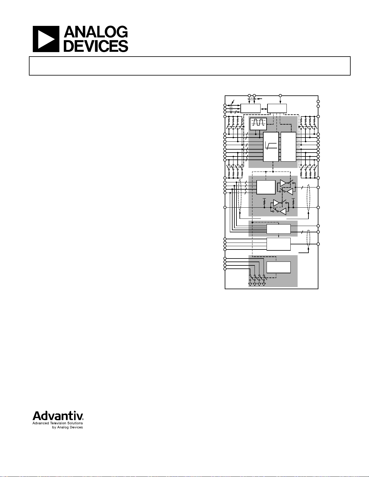
FUNCTIONAL BLOCK DIAGRAM
SEL[1:0] TX_EN
SERIAL
I2C_SDA
I2C_SCL
I2C_ADDR[ 1:0]
AVCC
IN_x_CLK+
IN_x_CLK–
IN_x_DATA2+
IN_x_DATA2–
IN_x_DATA1+
IN_x_DATA1–
IN_x_DATA0+
IN_x_DATA0–
AVCC
DDC_xxx_A
DDC_xxx_B
DDC_xxx_C
DDC_xxx_D
CEC_IN
P5V_A
P5V_B
P5V_C
P5V_D
HPD_A
HPD_B
HPD_C
HPD_D
+
–
+
–
+
–
+
–
2
CONFIG
INTERFACE
4
4
4
4
4
4
4
2
2
2
2
DDC/CEC
LOS
TMDS
EDID
PRODUCT HIGHLIGHTS
1. Input cable equalizer enables use of long cables at the input.
For a 24 AWG cable, the ADV3002 compensates for more
than 15 meters at data rates of up to 3 Gbps.
2. Auxiliary multiplexer isolates and buffers the DDC bus and
the CEC line, increasing total system capacitance limit.
3. EDID replication eliminates the need for multiple EDID
EEPROMs. EDID can be loaded from a single external
EEPROM or from a system microcontroller.
4. 5 V power combiner powers the EDID replicator and CEC
buffer when local system power is off.
5. Integrated hot plug detect pulse low on channel switch
with programmable pulse width or direct manual control.
RESETB
PARALLEL
CONTRO L
LOGIC
SWITCH
CORE
EQ
SWITCH
CORE
3.3V 3.3V
BIDIRECTI ONAL
REPLICATOR
CONTRO L
5V
COMBI NER
EDID EEPROM INTERFACE
HPD
CONTROL
HOT PLUG DETECT
Figure 1.
ADV3002
2
2
AVCC
AVEE
AVCC
+
OUT_CLK+
–
OUT_CLK–
+
OUT_DATA2+
–
OUT_DATA2–
+
OUT_DATA1+
–
OUT_DATA1–
+
OUT_DATA0+
–
OUT_DATA0–
AVCC
DDC_SCL_COM ,
DDC_SDA_COM
CEC_OUT
EDID_ENABLE
EDID_SCL,
EDID_SDA
AMUXVCC
07905-001
Rev. A
Information furnished by Analog Devices is believed to be accurate and reliable. However, no
responsibility is assumed by Anal og Devices for its use, nor for any infringements of p atents or other
rights of third parties that may result from its use. Specifications subject to chan ge without notice. No
license is granted by implication or otherwise under any patent or patent rights of Analog Devices.
Trademarks and registered trademarks are the property of their respective owners.
One Technology Way, P.O. Box 9106, Norwood, MA 02062-9106, U.S.A.
Tel: 781.329.4700 www.analog.com
Fax: 781.461.3113 ©2008–2011 Analog Devices, Inc. All rights reserved.

ADV3002
TABLE OF CONTENTS
Features.............................................................................................. 1
Applications....................................................................................... 1
General Description ......................................................................... 1
Functional Block Diagram .............................................................. 1
Product Highlights ........................................................................... 1
Revision History ............................................................................... 2
Specifications..................................................................................... 3
TMDS Performance Specifications............................................ 3
Auxiliary Channel Performance Specifications........................ 3
Power Supply and Control Logic Specifications ...................... 4
Absolute Maximum Ratings............................................................ 5
Thermal Resistance ...................................................................... 5
ESD Caution.................................................................................. 5
Pin Configuration and Function Descriptions............................. 6
Typical Performance Characteristics ............................................. 8
Theory of Operation ...................................................................... 12
TMDS Input Channels............................................................... 12
TMDS Output Channels ...........................................................12
DDC Buffers................................................................................ 13
EDID Replication....................................................................... 13
5 V Combiner ............................................................................. 15
CEC Buffer .................................................................................. 16
Hot Plug Detect Control ........................................................... 16
Loss of Signal Detect.................................................................. 16
Serial Control Interface ................................................................. 17
Reset ............................................................................................. 17
Write Procedure.......................................................................... 17
Read Procedure........................................................................... 18
Register Map ................................................................................... 19
Applications Information.............................................................. 21
HDMI Multiplexer for Advanced TV ..................................... 21
Cable Lengths and Equalization............................................... 24
PCB Layout Guidelines.............................................................. 24
Outline Dimensions....................................................................... 27
Ordering Guide .......................................................................... 27
REVISION HISTORY
8/11—Rev. 0 to Rev. A
Changed Data Rate = 2.25 Gbps to
Data Rate = 3 Gbps........................................................ Throughout
Changes to Features Section and Product Highlights Section ... 1
Changes to Table 1............................................................................ 3
Changes to Figure 4 Caption and Figure 6 Caption..................... 8
Added Figure 5 and Figure 7; Renumbered Sequentially ........... 8
Moved Figure 8 and Figure 10 ........................................................ 9
Changes to Figure 8 Caption and Figure 10 Caption .................. 9
Added Figure 9 and Figure 11......................................................... 9
Changes to Figure 12 and Figure 15............................................. 10
Changes to TMDS Input Channels Section and TMDS Output
Channels Section ............................................................................ 12
Changes to Figure 31...................................................................... 16
Changes to Cable Lengths and Equalization Section ................ 24
12/08—Revision 0: Initial Version
Rev. A | Page 2 of 28

ADV3002
SPECIFICATIONS
TA = 27°C, AVCC = 3.3 V, AMUXVCC = 5 V, AVEE = 0 V, data rate = 3 Gbps, differential input swing = 1000 mV, TMDS outputs
terminated with external 50 Ω resistors to 3.3 V, unless otherwise noted.
TMDS PERFORMANCE SPECIFICATIONS
Table 1.
Parameter Test Conditions/Comments Min Typ Max Unit
DYNAMIC PERFORMANCE
Maximum Data Rate (DR) per Channel NRZ 3 Gbps
Maximum Clock Rate 300 MHz
Bit Error Rate (BER) PRBS 223 − 1 10−9
Added Data Jitter DR ≤ 3 Gbps, PRBS 27 − 1 40 ps p-p
Added Clock Jitter 1 ps rms
Differential Intrapair Skew At output 1 ps
Differential Interpair Skew At output 35 ps
EQUALIZATION PERFORMANCE
High Frequency Gain Boost frequency = 1.5 GHz 16 dB
INPUT CHARACTERISTICS
Input Voltage Swing Differential 150 1200 mV
Input Common-Mode Voltage (V
OUTPUT CHARACTERISTICS
High Voltage Level Single-ended high speed channel AVCC − 200 AVCC + 10 mV
Low Voltage Level Single-ended high speed channel AVCC − 600 AVCC − 400 mV
Rise/Fall time (20% to 80%) DR = 3 Gbps 75 190 ps
TERMINATION
Input Termination Resistance Single-ended 50 Ω
Output Termination Resistance Single-ended 50 Ω
LOSS OF SIGNAL (LOS) DETECT
Frequency Cutoff LOS_FC (see Figure 31) 5 MHz
Amplitude Threshold
) AVCC − 800 AVCC mV
ICM
Clock rate = 300 MHz, LOS_THR = 00
35 mV
(see Figure 31)
AUXILIARY CHANNEL PERFORMANCE SPECIFICATIONS
Table 2.
Parameter Test Conditions/Comments Min Typ Max Unit
DDC CHANNELS
Input Capacitance, C
Input Low Voltage, VIL 0.5 V
Input High Voltage, VIH 0.7 × AMUXVCC V
Output Low Voltage, VOL IOL = 5 mA 0.25 0.4 V
Rise Time 10% to 90%, C
Fall Time 90% to 10%, C
Leakage VIN = 5.0 V 10 μA
DC bias = 2.5 V, ac voltage = 3.5 V p-p, f = 100 kHz 5 15 pF
AUX
= 50 pF, R
LOAD
= 50 pF, R
LOAD
= 2 kΩ 1.45 μs
PULL-UP
= 2 kΩ 20 250 ns
PULL-UP
Rev. A | Page 3 of 28

ADV3002
Parameter Test Conditions/Comments Min Typ Max Unit
CEC CHANNEL
Input Capacitance, C
Input Low Voltage, VIL 0.8 V
Input High Voltage, VIH 2.0 V
Output Low Voltage, VOL IOL = 3 mA 0.1 0.6 V
Output High Voltage, VOH 2.5 V
Rise Time
Fall Time
Pull-Up Resistance 26 kΩ
Leakage Off-leakage test conditions1 1.8 μA
HOT PLUG DETECT
Output Low Voltage, VOL RPU = 800 Ω 0.25 0.4 V
1
Off leakage test conditions are described in the HDMI Compliance Test Specification 1.3c Section 8, Test ID 8-14. To measure CEC leakage, connect the CEC line to
3.63 V via 26 kΩ ± 5 % resistor with an ammeter in series and with the power mains disabled.
POWER SUPPLY AND CONTROL LOGIC SPECIFICATIONS
Table 3.
Parameter Test Conditions/Comments Min Typ Max Unit
POWER SUPPLY
AVCC Operating range (3.3 V ± 10%) 3.0 3.3 3.6 V
P5V_x 4.7 5 5.5 V
AMUXVCC Output voltage, total load1 = 50 mA 4.0 5 5.5 V
QUIESCENT CURRENT
AVCC Outputs disabled 40 60 mA
Outputs enabled 170 150 mA
P5V_x Main power on 0.5 10 mA
Main power off 20 30 mA
AMUXVCC Main power on 20 30 mA
Main power off 0.5 10 mA
POWER DISSIPATION
Outputs disabled 232 381 mW
Outputs enabled 661 885 mW
I2C® AND LOGIC INPUTS2
Input High Voltage, VIH 2.4 V
Input Low Voltage, VIL 1.0 V
I2C AND LOGIC OUTPUTS2
Output High Voltage, VOH I
Output Low Voltage, VOL I
1
The total load current includes current drawn by the ADV3002 as well as external devices powered from the AMUXVCC supply.
2
The ADV3002 I2C control and logic input pins are listed as Control in the Type column in . I2C pins are 5 V tolerant and based on the 3.3 V I2C bus specification. Table 6
DC bias = 1.65 V, ac voltage = 2.5 V p-p, f = 100 kHz 5 15 pF
AUX
10% to 90%, C
= 3 kΩ
R
PULL-UP
90% to 10%, C
R
= 3 kΩ
PULL-UP
OH
OL
= 1500 pF, R
LOAD
= 1500 pF, R
LOAD
= 27 kΩ; or C
PULL-UP
= 27 kΩ; or C
PULL-UP
= 7200 pF,
LOAD
= 7200 pF,
LOAD
= −2 mA AVCC V
= +2 mA 0.4 V
75 250 μs
0.2 50 μs
Rev. A | Page 4 of 28
ADV3002
ABSOLUTE MAXIMUM RATINGS
Table 4.
Parameter Rating
AVCC to AVEE 3.7 V
P5V_x 5.8 V
AMUXVCC AVCC − 0.3 V < AMUXVCC < 5.8 V
Internal Power Dissipation 1.2 W
TMDS Single-Ended Input
Voltage
TMDS Differential Input
Voltage
Voltage at TMDS Output V
DDC Input Voltage AVEE − 0.3 V < VIN < AMUXVCC + 0.3 V
CEC Input Voltage AVEE − 0.3 V < VIN < 4.0 V
I2C Logic Input Voltage
(EDID_SCL, EDID_SDA,
I2C_SCL, I2C_SDA)
Parallel Input Voltage
(I2C_ADDR[1:0],
RESETB)
Parallel Input Voltage
(SEL[1:0], TX_EN)
Storage Temperature Range −65°C to +125°C
Operating Temperature
Range
Junction Temperature 150°C
ESD Protection (HBM) on
HDMI Input Pins
ESD Protection (HBM) on
All Other Pins
AVC C − 1.4 V < V
2.0 V
< 3.7 V
OUT
AVEE − 0.3 V < V
AVEE − 0.3 V < V
AVEE − 0.3V < V
0°C to +85°C
±8 kV
±2.5 kV
< AVCC + 0.3 V
IN
< 4.0 V
IN
< AMUXVCC + 0.3 V
IN
< AVCC + 0.3 V
IN
Stresses above those listed under Absolute Maximum Ratings
may cause permanent damage to the device. This is a stress
rating only; functional operation of the device at these or any
other conditions above those indicated in the operational
section of this specification is not implied. Exposure to absolute
maximum rating conditions for extended periods may affect
device reliability.
THERMAL RESISTANCE
θJA is specified for the worst-case conditions; a device soldered
in a 4-layer JEDEC circuit board for surface-mount packages.
θ
is specified for the exposed pad soldered to the circuit board
JC
with no airflow.
Table 5. Thermal Resistance
Package Type θJA θ
80-Lead LQFP (ST-80-2) 51.3 15.3 °C/W
Unit
JC
ESD CAUTION
Rev. A | Page 5 of 28
ADV3002
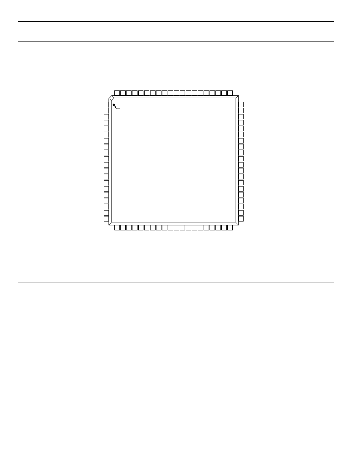
PIN CONFIGURATION AND FUNCTION DESCRIPTIONS
P5V_A79P5V_B78P5V_C77P5V_D76DDC_SDA_A75DDC_SCL_A74DDC_SDA_B73DDC_SCL_B72DDC_SDA_C71DDC_SCL_C70DDC_SDA_D69DDC_SCL_D68DDC_SDA_COM67DDC_SCL_COM66CEC_IN65CEC_OUT64AMUXVCC63EDID_ENABLE62EDID_SDA61EDID_SCL
80
39
40
I2C_ADDR1
I2C_SDA
60
IN_C_DATA2+
59
IN_C_DATA2–
58
HPD_C
57
IN_C_DATA1+
56
IN_C_DATA1–
55
HPD_D
54
IN_C_DATA0+
53
IN_C_DATA0–
52
AVC C
51
IN_C_CLK+
50
IN_C_CLK–
49
I2C_ADDR0
48
IN_D_DATA2+
47
IN_D_DATA2–
46
AVE E
45
IN_D_DATA1+
44
IN_D_DATA1–
43
AVC C
42
IN_D_DATA0+
41
IN_D_DATA0–
IN_B_CLK–
IN_B_CLK+
HPD_B
IN_B_DATA0–
IN_B_DATA0+
HPD_A
IN_B_DATA1–
IN_B_DATA1+
AVC C
IN_B_DATA2–
IN_B_DATA2+
SEL0
IN_A_CLK–
IN_A_CLK+
SEL1
IN_A_DATA0–
IN_A_DATA0+
AVC C
IN_A_DATA1–
IN_A_DATA1+
1
PIN 1
2
3
4
5
6
7
8
9
10
11
12
13
14
15
16
17
18
19
20
21
22
24
25
23
AVE E
TX_EN
IN_A_DATA2+
OUT_DATA2+
IN_A_DATA2–
26
27
OUT_DATA2–
ADV3002
(Not to Scale)
28
29
I2C_SCL
OUT_DATA1+
TOP VIEW
30
31
AVE E
OUT_DATA1–
33
34
35
36
32
AVC C
OUT_CLK+
OUT_DATA0–
OUT_DATA0+
38
37
RESETB
OUT_CLK–
IN_D_CLK–
IN_D_CLK+
Figure 2. Pin Configuration
Table 6. Pin Function Descriptions
Pin No. Mnemonic Type Description
1 IN_B_CLK− TMDS High Speed TMDS Input B Clock Complement.
2 IN_B_CLK+ TMDS High Speed TMDS Input B Clock.
3 HPD_B HPD Hot Plug Detect Output B.
4 IN_B_DATA0− TMDS High Speed TMDS Input B Data Complement.
5 IN_B_DATA0+ TMDS High Speed TMDS Input B Data.
6 HPD_A HPD Hot Plug Detect Output A.
7 IN_B_DATA1− TMDS High Speed TMDS Input B Data Complement.
8 IN_B_DATA1+ TMDS High Speed TMDS Input B Data.
9, 18, 33, 43, 52 AVCC Power Positive Analog Supply 3.3 V.
10 IN_B_DATA2− TMDS High Speed TMDS Input B Data Complement.
11 IN_B_DATA2+ TMDS High Speed TMDS Input B Data.
12 SEL0 Control Channel Select Parallel Control LSB.
13 IN_A_CLK− TMDS High Speed TMDS Input A Clock Complement.
14 IN_A_CLK+ TMDS High Speed TMDS Input A Clock.
15 SEL1 Control Channel Select Parallel Control MSB.
16 IN_A_DATA0− TMDS High Speed TMDS Input A Complement.
17 IN_A_DATA0+ TMDS High Speed TMDS Input A Data.
19 IN_A_DATA1− TMDS High Speed TMDS Input A Data Complement.
20 IN_A_DATA1+ TMDS High Speed TMDS Input A Data.
21, 30, 46 AVEE Power Negative Analog Supply 0.0 V.
22 IN_A_DATA2− TMDS High Speed TMDS Input A Data Complement.
23 IN_A_DATA2+ TMDS High Speed TMDS Input A Data.
Rev. A | Page 6 of 28
07905-002

ADV3002
Pin No. Mnemonic Type Description
24 TX_EN Control TMDS Output Enable Parallel Control.
25 OUT_DATA2+ TMDS High Speed TMDS Output.
26 OUT_DATA2− TMDS High Speed TMDS Output Complement.
27 I2C_SCL Control Serial Control Clock Input.
28 OUT_DATA1+ TMDS High Speed TMDS Output.
29 OUT_DATA1− TMDS High Speed TMDS Output Complement.
31 OUT_DATA0+ TMDS High Speed TMDS Output.
32 OUT_DATA0− TMDS High Speed TMDS Output Complement.
34 OUT_CLK+ TMDS High Speed TMDS Output Clock.
35 OUT_CLK− TMDS High Speed TMDS Output Clock Complement.
36 RESETB Control Configuration Registers Reset. Active low.
37 IN_D_CLK− TMDS High Speed TMDS Input D Clock Complement.
38 IN_D_CLK+ TMDS High Speed TMDS Input D Clock.
39 I2C_ADDR1 Control Serial Control External Address MSB.
40 I2C_SDA Control Serial Control Data Input/Output.
41 IN_D_DATA0− TMDS High Speed TMDS Input D Data Complement.
42 IN_D_DATA0+ TMDS High Speed TMDS Input D Data.
44 IN_D_DATA1− TMDS High Speed TMDS Input D Data Complement.
45 IN_D_DATA1+ TMDS High Speed TMDS Input D Data.
47 IN_D_DATA2− TMDS High Speed TMDS Input D Data Complement.
48 IN_D_DATA2+ TMDS High Speed TMDS Input D Data.
49 I2C_ADDR0 Control Serial Control External Address LSB.
50 IN_C_CLK− TMDS High Speed TMDS Input C Clock Complement.
51 IN_C_CLK+ TMDS High Speed TMDS Input C Clock.
53 IN_C_DATA0− TMDS High Speed TMDS Input C Data Complement.
54 IN_C_DATA0+ TMDS High Speed TMDS Input C Data.
55 HPD_D HPD Hot Plug Detect Output D.
56 IN_C_DATA1− TMDS High Speed TMDS Input C Data Complement.
57 IN_C_DATA1+ TMDS High Speed TMDS Input C Data.
58 HPD_C HPD Hot Plug Detect Output C.
59 IN_C_DATA2− TMDS High Speed TMDS Input C Data Complement.
60 IN_C_DATA2+ TMDS High Speed TMDS Input C Data.
61 EDID_SCL Control External EDID EEPROM Serial Interface Clock.
62 EDID_SDA Control External EDID EEPROM Serial Interface Data.
63 EDID_ENABLE Control EDID Replication Enable.
64 AMUXVCC Power Positive Power Supply 5.0 V.
65 CEC_OUT CEC Consumer Electronics Control Output.
66 CEC_IN CEC Consumer Electronics Control Input.
67 DDC_SCL_COM DDC Display Data Channel Serial Clock Common Input/Output.
68 DDC_SDA_COM DDC Display Data Channel Serial Data Common Input/Output.
69 DDC_SCL_D DDC Display Data Channel Serial Clock Input/Output D.
70 DDC_SDA_D DDC Display Data Channel Serial Data Input/Output D.
71 DDC_SCL_C DDC Display Data Channel Serial Clock Input/Output C.
72 DDC_SDA_C DDC Display Data Channel Serial Data Input/Output C.
73 DDC_SCL_B DDC Display Data Channel Serial Clock Input/Output B.
74 DDC_SDA_B DDC Display Data Channel Serial Data Input/Output B.
75 DDC_SCL_A DDC Display Data Channel Serial Clock Input/Output B.
76 DDC_SDA_A DDC Display Data Channel Serial Data Input/Output A.
77 P5V_D Power 5 V HDMI Supply from Source D.
78 P5V_C Power 5 V HDMI Supply from Source C.
79 P5V_B Power 5 V HDMI Supply from Source B.
80 P5V_A Power 5 V HDMI Supply from Source A.
Rev. A | Page 7 of 28
ADV3002
V
V
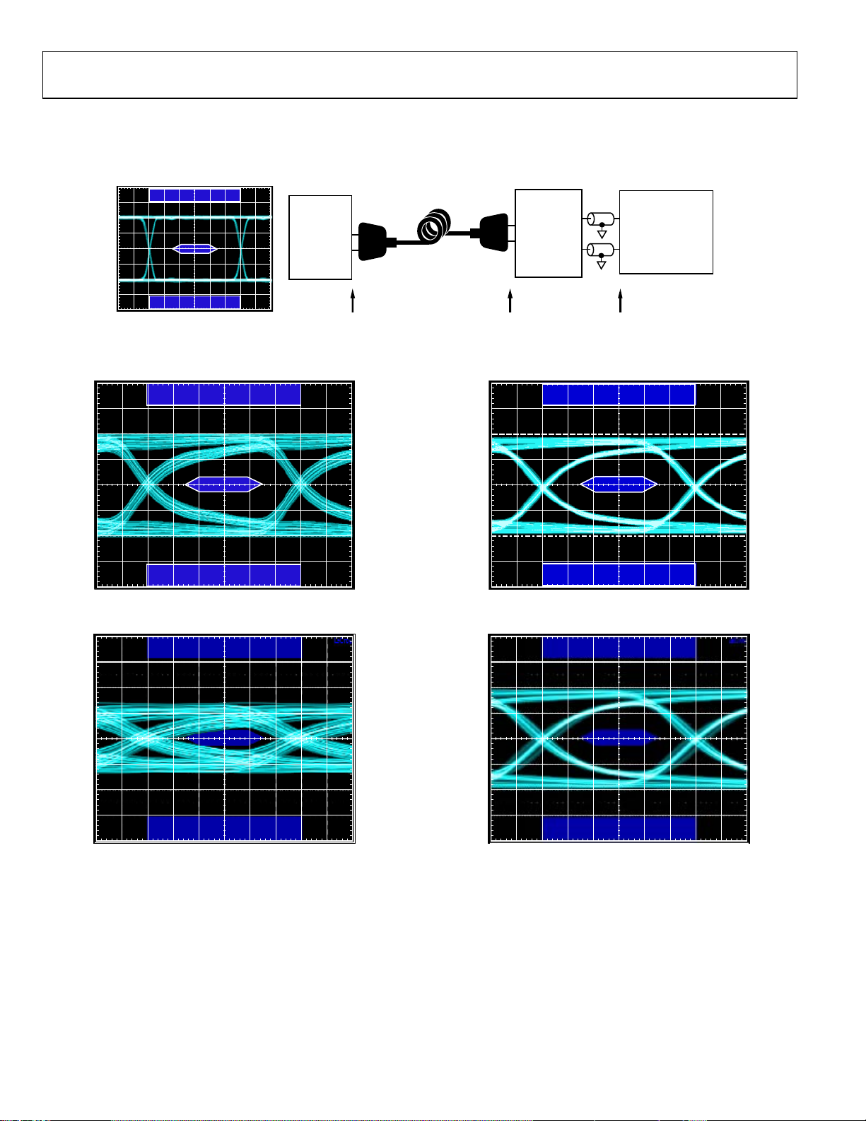
TYPICAL PERFORMANCE CHARACTERISTICS
TA = 27°C, AVCC = 3.3 V, AMUXVCC = 5.0 V, AVEE = 0 V, differential input swing = 1000 mV, pattern = PRBS 27 − 1, data rate = 3 Gbps,
TMDS outputs terminated with external 50 resistors to 3.3 V, unless otherwise noted.
HDMI CABLE
DIGITAL
PATTERN
GENERATOR
ADV3002
EVALUATIO N
BOARD
SMA COAX CABLE
SERIAL DATA
ANALYZER
REFERENCE EYE DI AGRAM AT TP1
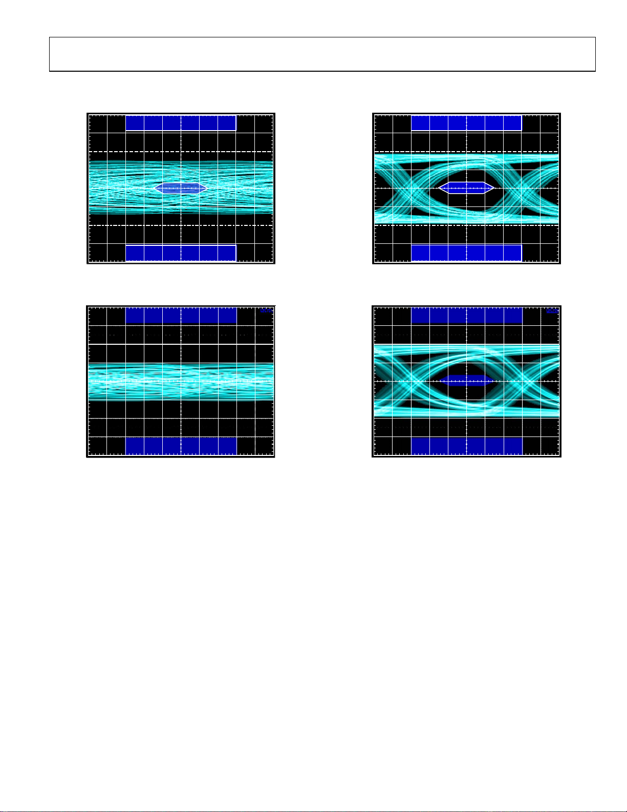
Figure 3. Test Circuit for Eye Diagrams
250mV/DI
0.167UI/DI V AT 2.25Gb ps
Figure 4. Eye Diagram at TP2 for 2 Meter Cable, Data Rate = 2.25 Gbps
TP1 TP2 TP3
250mV/DI
07905-022
0.167UI/DI V AT 2.25Gbps
Figure 6. Eye Diagram at TP3 for 2 Meter Cable, Data Rate = 2.25 Gbps
07905-021
07905-024
250mV/DIV
0.167UI/DIV AT 3.0Gbps
Figure 5. Eye Diagram at TP2 for 2 Meter Cable, Data Rate = 3 Gbps
07905-205
250mV/DIV
0.167UI/DIV AT 3.0Gbps
Figure 7. Eye Diagram at TP3 for 2 Meter Cable, Data Rate = 3 Gbps
07905-207
Rev. A | Page 8 of 28
ADV3002
V
V
TA = 27°C, AVCC = 3.3 V, AMUXVCC = 5.0 V, AVEE = 0 V, differential input swing = 1000 mV, pattern = PRBS 27 − 1, data rate = 3 Gbps,
TMDS outputs terminated with external 50 resistors to 3.3 V, unless otherwise noted.
250mV/DI
0.167UI/DI V AT 2.25Gb ps
07905-023
Figure 8. Eye Diagram at TP2 for 20 Meter 24 AWG Cable,
Data Rate = 2.25 Gbps
250mV/DIV
0.167UI/DIV AT 3.0Gbps
07905-209
Figure 9. Eye Diagram at TP2 for15 Meter 24 AWG Cable, Data Rate = 3 Gbps
250mV/DI
0.167UI/DI V AT 2.25Gbps
Figure 10. Eye Diagram at TP3 for 20 Meter 24 AWG Cable,
Data Rate = 2.25 Gbps
250mV/DIV
0.167UI/DIV AT 3.0Gbps
Figure 11. Eye Diagram at TP3 for 15 Meter 24 AWG Cable,
Data Rate = 3 Gbps
07905-025
07905-211
Rev. A | Page 9 of 28

ADV3002
TA = 27°C, AVCC = 3.3 V, AMUXVCC = 5.0 V, AVEE = 0 V, differential input swing = 1000 mV, pattern = PRBS 27 − 1, data rate = 3 Gbps,
TMDS outputs terminated with external 50 resistors to 3.3 V, unless otherwise noted.
1.0
ALL CABLES = 24 AWG
0.9
0.8
0.7
0.6
0.5
0.4
0.3
DETERMINISTIC JITTER (UI)
0.2
0.1
0
0 10203
1080p, 12-BI T
1080p, 10-BI T
1080p, 8-BI T
720p
3Gbps
INPUT CABLE L ENGTH (m)
0
07905-026
Figure 12. Jitter vs. Input Cable Length
100
90
80
70
60
50
40
JITTER (ps)
30
20
10
0
0 0.5 1.0 1.5 2.0 2.5 3.0 3.5
DETERMINISTIC JITTER
RANDOM JITT ER
DATA RATE (Gbp s)
07905-027
Figure 13. Jitter vs. Data Rate
100
90
80
70
60
50
40
JITTER (ps)
30
20
10
0
2.0 2.2 2.4 2.6 2.8 3.0 3.2 3.4 3.6
DETERMINISTIC JITTER
RANDOM JITT ER
SUPPLY VOLTAGE (V)
07905-028
Figure 14. Jitter vs. Supply Voltage
100
90
80
70
60
50
40
JITTER (ps)
30
20
10
0
0 1020304050607080
DETERMINISTIC JITTER
RANDOM JITTER
TEMPERATURE (° C)
Figure 15. Jitter vs. Temperature
1000
800
600
400
EYE HEIGHT (mV)
200
0
0 0.5 1.0 1.5 2.0 2.5 3.0 3.5
DATA RATE (Gb ps)
Figure 16. Eye Height vs. Data Rate
1000
800
600
400
EYE HEIGHT (mV)
200
0
2.0 2.2 2.4 2.6 2.8 3. 0 3.2 3.4 3.6
SUPPLY VOLTAGE (V)
Figure 17. Eye Height vs. Supply Voltage
07905-029
07905-030
07905-031
Rev. A | Page 10 of 28

ADV3002
100
90
80
70
60
50
40
30
DETERMINISTIC JITTER (ps)
20
10
0
0 0.2 0.4 0.6 0.8 1.0 1.2 1.4 1.6 1.8 2.0
EQ = 18dB
DIFFERENTIAL INPUT SWING (V)
Figure 18. Deterministic Jitter vs. Input Swing
250
07905-032
100
90
80
70
60
50
40
JITTER (ps)
30
20
10
0
2.0 2.2 2.4 2.6 2.8 3.0 3.2 3.4 3.6
DETERMINISTIC JITTER
RANDOM JITT ER
INPUT COMMON-MODE VOLT AGE (V)
Figure 21. Jitter vs. Input Common-Mode Voltage
0.6
07905-035
200
150
100
RISE/FALL TIME (ps)
50
0
0 1020304050 607080
DATA RI SE TIME @ 2 .25Gb ps
DATA FALL TIME @ 2.25Gbps
CLOCKRISETIME@225MHz
CLOCK FALL TIME @ 225MHz
TEMPERATURE (°C)
Figure 19. Rise/Fall Time vs. Temperature
100
90
80
70
60
50
40
30
20
TERMINATION RESISTANCE ( Ω)
10
0
0 10 20304050 607080
TEMPERATURE (° C)
07905-033
07905-034
0.5
0.4
0.3
0.2
0.1
OUTPUT LOGIC LOW VOLTAG E (V)
0
02468
LOAD CURRENT (mA)
DDC
CEC
HPD
10
07905-036
Figure 22. Output Logic Low Voltage vs. Load Current (DDC, CEC, and HPD)
Figure 20. Termination Resistance vs. Temperature
Rev. A | Page 11 of 28

ADV3002
A
V
A
V
THEORY OF OPERATION
The primary function of the ADV3002 is to switch up to four
HDMI/DVI sources to one HDMI/DVI sink. Each HDMI/DVI
link consists of four differential, high speed channels and four
auxiliary single-ended, low speed signals. The high speed channels
include a data-word clock and threeTMDS data channels running
at 10× the data-word clock frequency for data rates up to 3 Gbps.
The four low speed control signals are the display data channel
(DDC) bus (SDA and SCL), the consumer electronics control
(CEC) line, and the hot plug detect (HPD) signal.
The ADV3002 also includes an integrated EDID SRAM,
eliminating the need for an external EDID EEPROM for each
HDMI connector. A typical HDMI multiplexer is shown in
Figure 23. The simplified implementation using the ADV3002
is shown in Figure 24.
DDC
5V
HDMI A
HDMI B
HDMI C
HDMI D
HDMI A
HDMI B
DDC
5V
DDC
5V
DDC
5V
DDC
5V
DDC
5V
DDC
EDID A
EDID B
EDID C
EDID D
2
2
4:1
HDMI
2
2
MUX
2
DDC
Figure 23. Typical HDMI Multiplexer
2
2
ADV3002
2
2
DDC
HDMI
Rx
HDMI
Rx
07905-003
TMDS INPUT CHANNELS
Each high speed input differential pair terminates to the 3.3 V
power supply through a pair of 50 Ω on-chip resistors, as shown
in Figure 25. The state of the input terminations can be configured
automatically or programmed manually by setting the appropriate
bits in the TMDS input termination control register, as shown
in Tabl e 10 .
The input equalizer can be manually configured to provide two
different levels of high frequency boost: 4 dB or 16 dB for 3 Gbps
data. The equalizer (EQ) level defaults to 16 dB after reset. No
specific cable length is suggested for a particular equalization
setting because cable performance varies widely between manufacturers; however, in general, the equalization of the ADV3002
can be set to 16 dB without degrading the signal integrity, even for
short input cables.
CC
50Ω 50Ω
IN+
IN–
AVEE
NOTES
1. IN+ REF ERS TO IN_x_CLK+/ IN_x_D ATAx+ PINS.
2. IN– REFERS TO IN_x_CLK–/IN_x_D ATAx– PINS.
Figure 25. High Speed Input Simplified Schematic
CABLE
EQ
07905-005
TMDS OUTPUT CHANNELS
Each high speed output differential pair is terminated to the 3.3 V
power supply through a pair of 50 Ω on-chip resistors, as shown
in Figure 26. This termination is user-selectable; it can be
turned on or off by programming the TX_OTO bit of the TMDS
output control register, as shown in Tab l e 10 .
CC
5V
HDMI C
DDC
5V
HDMI D
Figure 24. Simplified Implementation Using the ADV3002
2
2
AMUXVCC
MICROCONTROLLER
EDID DDC
EXTERNAL
EDID EEPROM
OR SYSTEM
07905-004
OUT+ OUT–
NOTES
1. OUT+ REF ERS TO OUT_CLK+ AND OUT_D ATAx+ PINS.
2. OUT– REF ERS TO OUT_CLK– AND OUT_D ATAx– PINS.
Figure 26. High Speed Output Simplified Schematic
The output termination resistors of the ADV3002 back
terminate the output TMDS transmission lines. These back
terminations, as recommended in the HDMI 1.4 specification,
act to absorb reflections from impedance discontinuities on the
output traces, improving the signal integrity of the output traces
and adding flexibility to how the output traces can be routed.
50Ω 50Ω
DISABLE I
AVEE
OUT
ESD
PROT.
07905-006
Rev. A | Page 12 of 28

ADV3002
For example, interlayer vias can be used to route the ADV3002
TMDS outputs on multiple layers of the printed circuit board
(PCB) without severely degrading the quality of the output signal.
The output has a disable feature that places the outputs in tristate
mode. Bigger wire-OR’ed arrays can be constructed using the
ADV3002 in this mode.
The ADV3002 requires output termination resistors when the high
speed outputs are enabled. Termination can be internal and/or
external. The internal terminations of the ADV3002 are enabled
by default after reset. External terminations can be provided either
by on-board resistors or by the input termination resistors of an
HDMI/DVI receiver. If both the internal terminations are enabled
and external terminations are present, set the output current level
to 20 mA by programming the TX_OCL bit of the TMDS output
control register, as shown in Tabl e 10 (20 mA is the default
upon reset). If only external terminations are provided (if the
internal terminations are disabled), set the output current level
to 10 mA by programming the TX_OCL bit of the TMDS output
control register. The high speed outputs must be disabled if
there are no output termination resistors present in the system.
DDC BUFFERS
The DDC buffers are 5 V tolerant bidirectional lines that carry
extended display identification data (EDID) and high bandwidth
digital content protection (HDCP) encryption. The ADV3002
provides switching and buffering for the DDC buses. The DDC
buffers are bidirectional, and fully support arbitration, clock
synchronization, and other relevant features of a standard
2
mode I
C bus.
EDID REPLICATION
The ADV3002 EDID replication feature reduces the total system
cost by eliminating the need for an EDID EEPROM for each
HDMI port. With the ADV3002, only a single external EDID is
necessary. The ADV3002 stores the EDID information in an
on-chip SRAM. This enables the EDID information to be
simultaneously accessible to all four HDMI ports. The ADV3002
combines the 5 V power from the four HDMI sources such that
the EDID information can be available even when the system
power is off. A block diagram of the ADV3002 DDC buffering
and EDID replication scheme is shown in Figure 27.
HDMI
PORT A
HDMI
PORT B
HDMI
PORT C
HDMI
PORT D
SRAM
2
I
C
MASTER
EDID
CONTROL
2
I
C
READ/
WRITE
SLAVE
2
2
2
2
2
I
C
READ
SLAVE
2
I
C
READ
SLAVE
2
I
C
READ
SLAVE
2
2
DDC
MUX
2
2
2
I
C
READ/
WRITE
SLAVE
22
EDID_[SCL/SDA]
2
2
I2C_[SCL /SDA]
HDMI
Rx
EXTERNAL
EDID
EEPROM
v1.3
MCU
07905-007
Figure 27. EDID Replication Block Diagram
Rev. A | Page 13 of 28

ADV3002
Source Physical Address Assignment
In HDTV applications where the CEC function is available, the
EDID contains the source physical address (SPA); a unique value
for each HDMI port. Because the memory in the ADV3002 is
volatile, the SPA must be stored in the external EDID EEPROM.
Rather than require a larger external EEPROM to store the SPA,
because all 256 bytes of memory are needed for typical EDID
information, the ADV3002 takes advantage of EDID information
that is always a fixed value, such as the 24-bit IEEE registration
identifier (0x000C03). The 24 bits of the IEEE registration identifier
are replaced with the desired SPA values. When a source requests
the IEEE registration identifier, the ADV3002 responds with the
fixed value (0x000C03). The ADV3002 then automatically
calculates the correct checksum for each port based on the SPA
stored for that port in the vendor specific data block (VSDB).
CEC-enabled devices have a source physical address (SPA) that
allows the CEC controller to address the specific physical devices
and control switches. The SPA is comprised of four fields or
nibbles. Each field is a 4-bit number; therefore, each field can be
any one of 16 possible values (0x0 through 0xF). Each HDMI
input port is assigned a unique SPA as shown in Figure 28. In
any CEC-enabled device, only one of the four fields is unique
per port. In HDMI sink applications, where the sink is the root
device, only the W field is unique per port, whereas the X, Y,
and Z fields are always set to zero.
SPA = W. X. Y. Z
A typical vendor specific data block (VSDB) is shown in Table 7.
When using the ADV3002 EDID replicator, the VSDB should
be replaced with the one shown in Table 8, whereby the port
specific field can be assigned to any of the four fields (W, X, Y, or Z)
depending on the value set in the override select bits as shown
in Table 9.
When calculating the checksum for Block 1 of the EDID, do not
use the custom values entered in place of the IEEE registration
identifier in the calculation; instead, use the IEEE registration
identifier values (0x000C03). Include the values in Byte 4 and
Byte 5 of the VSDB in the calculation.
Table 7. Typical Vendor Specific Data Block (VSDB)
Byte No. 7 6 5 4 3 2 1 0
0
1
2
3
4 SPA Field W SPA Field X
5 SPA Field Y SPA Field Z
6 to N Remainder or VSDB is stored in Byte 6 through Byte N
Table 8. Vendor Specific Data Block with ADV3002
Byte No. 7 6 5 4 3 2 1 0
0
1 Port A SPA override field Port B SPA override field
2 Port C SPA override field Port D SPA override field
3 Not used Override select (see Table 9)
4 Default W field Default X field
5 Default Y field Default Z field
6 to N Remainder or VSDB is stored in Byte 6 through Byte N
Table 9. Override Select Assignment
Override Select
Bit 3 Bit 2 Bit 1 Bit 0
1 0 0 0 W
0 1 0 0 X
0 0 1 0 Y
0 0 0 1 Z
HDMI
PORT A
SPA = W
. XA.YA. Z
A
HDMI
PORT B
SPA = W
B
HDMI
PORT C
SPA = W
C
HDMI
PORT D
SPA = W
D
Figure 28. SPA Assignments
Vendor specific tag
. XB.YB. Z
. XC.YC. Z
. XD.YD. Z
A
B
ADV3002
C
D
07905-008
Length (= N)
code (= 3)
24-bit IEEE registration identifier (0x000C03)
(least significant byte first)
Vendor specific
Length (= N)
tag code (= 3)
Field Replaced by
Port-Specific SPA
Rev. A | Page 14 of 28

ADV3002
EDID Replication with External EEPROM
The ADV3002 has dedicated pins to interface to an external
EDID EEPROM: EDID_SDA and EDID_SCL. In the default
configuration, after the first hot plug event or system power-up,
the internal I
2
C master in the ADV3002 copies the contents of
the external EDID EEPROM into the on-chip SRAM. While the
EDID is being copied, the HPD signals for all four ports are held
low by the ADV3002. A flowchart of the start-up procedure is
shown in Figure 29. The entire start-up procedure takes less than
10 ms. The EDID replication feature can be disabled using the
EDID_ENABLE pin.
POWER-UP, RESET,
OR FIRST HOT PLUG
<100µs
COPY EDID INFORMATION
<10ms
Figure 29. EDID Replication Start-Up Flowchart with External EEPROM
WAIT
FOR EDID POWER-UP
TO ADV3002 SRAM
DETERMINE SPA
AND CHECKSUM
WAIT FOR EDID
REQUEST
RESPOND TO EDID
REQUEST
HPD ALL PORTS = L OW
HPD ALL PORTS = HI GH
Writing to the EDID EEPROM
The EDID data can be written to the external EEPROM by
2
writing data via the I
C control interface or via the HDMI A
DDC inputs. In both cases, the EDID write procedure is as
follows:
1. Write Value 0x96 to the EDID EEPROM write protect
password register, Register 0x0F. The ADV3002 fixed part
address is required to write to this register.
2. Write the EDID data to the EEPROM fixed part address.
Data must be written one byte at a time.
3. Write Value 0x00 to the EDID EEPROM write protect
password register, Register 0x0F.
07905-009
EDID Replication with External Microcontroller
The on-chip SRAM can be preloaded using an external microcontroller. Prior to loading the SRAM, disable the I
2
C master by
writing 0x01 to the EDID replication mode register, Register 0x0E.
The microcontroller can then write EDID information into the
SRAM via the ADV3002 I
2
C control interface. The writes to the
SRAM should be to the fixed part address of 0xA0. When the
EDID copy process is complete, enable the EDID replication
function by writing 0x00 to the EDID replication mode register
(Register 0x0E). The EDID_SDA and EDID_SCL pins are
unused when an external microcontroller is used to program
the SRAM. These pins can be tied either high or low through a
resistor, but should not be left floating.
Reset
Pullling the RESETB pin low initiates a restart of the EDID
replication procedure shown in Figure 29 when the local system
supply is on. If the local system supply is off, the RESETB pin
has no effect.
5 V COMBINER
The 5 V combiner circuit combines the four 5 V supplies from
the four HDMI sources and provides the necessary power to the
ADV3002 EDID replication circuit, the CEC buffer, as well as
the external EDID EEPROM, if applicable. The combiner circuit is
designed such that the current limits on each of the 5 V supplies
are not exceeded when the local system power is either on or off.
A simplified circuit diagram of the 5 V combiner is shown in
Figure 30. The combiner detects the presence of the voltage on
the 5 V pin (P5V_x) from the HDMI connectors and closes the
respective internal switch to connect the 5 V to AMUXVCC. If
the local system 3.3 V and 5 V supplies are available, then the
combiner opens all the switches.
DETECT
P5V_A
DETECT
P5V_B
DETECT
P5V_C
DETECT
P5V_D
Figure 30. 5 V Combiner Simplified Circuit Diagram
AMUXVCC
07905-010
Rev. A | Page 15 of 28

ADV3002
1
0
1
0
FD
LOS_FC
AD
LOS_THR
LOS_STATUS[3:0]
07905-011
CEC BUFFER
The CEC buffer is bidirectional and includes integrated on-chip
pull-up resistors. The CEC buffer isolates capacitance from the
PCB and local system microcontroller, which is particularly
advantageous in systems where the microcontroller is not placed
near the HDMI connectors. The integrated on-chip pull-up
resistors are connected to an internal 3.3 V supply that is generated
from the AMUXVCC supply; thus, the CEC buffer is fully compliant
with the CEC line degradation specifications, when the local
system power supply is either on or off.
HOT PLUG DETECT CONTROL
The HPD lines going into the ADV3002 are normally high
impedance but are pulled low for greater than 100 ms when a
channel switch occurs. This pull-down pulse width can be
changed by modifying the value in the hot plug detect pulse
width control register (Register 0x05), as shown in Tab l e 10 .
Also, the HPD pulse can be manually controlled using the hot
plug detect manual override control register (Register 0x06), as
shown in Tab l e 10 .
LOSS OF SIGNAL DETECT
The TMDS clock line of each HDMI input has a loss of signal
(LOS) monitor attached to it. The purpose of the LOS monitor
is to determine if there is activity in the HDMI link. A simplified
circuit diagram of the LOS detector is shown in Figure 31. The
LOS monitors are disabled by default. The LOS monitors can be
enabled by programming the LOS_EN bit of the LOS detect control
register (Register 0x07). When enabled, the status of each HDMI
input can be read in the LOS detect status register (Register 0x10).
A logic high LOS_STATUS bit of a given HDMI input indicates
an inactive input; a logic low LOS_STATUS bit indicates an
active input. Three conditions need to be fulfilled for an HDMI
input to be considered active:
FREQUENCY
TMDS CLO CK
INPUT[x]
Figure 31. Loss of Signal Detect Simplified Circuit Diagram
DETECTO R
AMPLIT UDE
DETECTO R
LOS Autosquelch
The LOS detect circuit can be used to automatically disable the
TMDS signal path. Setting the LOS_RX_EN bit in the LOS
control register (Register 0x07) causes the selected TMDS input
to be disabled when an LOS event occurs on that input. In this
case, the TMDS signal path is enabled when the active signal
conditions previously listed are met.
• The TMDS input termination resistors must be enabled. By
default, the ADV3002 TMDS input termination resistors
are enabled only on the selected input.
• The TMDS clock frequency exceeds the frequency cutoff
(LOS_FC). Refer to Tab l e 1 for the value of the LOS frequency
cutoff.
• TMDS clock differential amplitude exceeds the LOS threshold
set in the LOS detect control register (Register 0x07). Refer
to Tab l e 1 for the value of the LOS amplitude threshold.
Rev. A | Page 16 of 28

ADV3002
SERIAL CONTROL INTERFACE
RESET
On initial power-up, or at any point in operation, the ADV3002
register set can be restored to the default values by pulling the
RESETB pin low according to the specification in Tabl e 3.
During normal operation, however, the RESETB pin must
be pulled up to 3.3 V.
WRITE PROCEDURE
To write data to the ADV3002 register set, an I2C master (such
as a microcontroller) needs to send the appropriate control
signals to the ADV3002 slave device. The signals are controlled
2
by the I
the procedure, see Figure 32. The steps for a write procedure are
as follows:
1. Send a start condition (while holding the I2C_SCL line
2. Send the ADV3002 part address (seven bits). The upper five
3. Send the write indicator bit (0).
4. Wait f or t he ADV3002 to acknowledge the request.
5. Send the register address (eight bits) to which data is to be
C master, unless otherwise specified. For a diagram of
high and pulling the I2C_SDA line low).
bits of the ADV3002 part address are the static value [10010]
and the two LSBs are set by Input Pins I2C_ADDR[1:0].
This transfer should be MSB first.
written. This transfer should be MSB first.
I2C_SCL
GENERAL CASE
I2C_SDA
EXAMPLE
I2C_SDA
*THE SWITCHING/UPDATE DELAY BEGINS AT THE FALLING EDGE OF THE LAST DATA BIT;
FOR EXAMPLE, THE FALLING EDGE JUST BEFORE STEP 8.
START FIXED ADDR PART REGIS TER ADDR DATA STOP
1 2 3 4 5 6 7 8 9
R/W
ACK ACKADDR
Figure 32. I C Write Procedure
2
6. Wait f or t he ADV3002 to acknowledge the request.
7. Send the data (eight bits) to be written to the register
whose address was set in Step 5. This transfer should be
MSB first.
8. Wait f or t he ADV3002 to acknowledge the request.
9. Do one of the following:
a. Send a stop condition (while holding the I2C_SCL
line high and pulling the I2C_SDA line high) and
release control of the bus to end the transaction
(shown in Figure 32).
b. Send a repeated start condition (while holding the
I2C_SCL line high and pulling the I2C_SDA line low)
and continue from Step 2 in this procedure to perform
another write.
c. Send a repeated start condition (while holding the
I2C_SCL line high and pulling the I2C_SDA line low)
and continue from Step 2 of the read procedure (in the
Read Procedure section) to perform a read from
another address.
d. Send a repeated start condition (while holding the
I2C_SCL line high and pulling the I2C_SDA line low)
and continue from Step 8 of the read procedure (in the
Read Procedure section) to perform a read from the
same address set in Step 5 of the write procedure.
*
ACK
07905-012
Rev. A | Page 17 of 28

ADV3002
I2C_SCL
GENERAL CASE
I2C_SDA
EXAMPLE
I2C_SDA
FIXED PART
START
1 2 3 4 5 6 7 8 9 10 11 12 13
ADDR
ADDR
R/W
REGISTER ADDR
ACK
Figure 33. I C Read Procedure
READ PROCEDURE
To read data from the ADV3002 register set, an I2C master
(such as a microcontroller) needs to send the appropriate
control signals to the ADV3002 slave device. The signals are
controlled by the I
diagram of the procedure, see Figure 33. The steps for a read
procedure are as follows:
1. Send a start condition (while holding the I2C_SCL line
high and pulling the I2C_SDA line low).
2. Send the ADV3002 part address (seven bits). The upper five
bits of the ADV3002 part address are the static value [10010]
and the two LSBs are set by Input Pins I2C_ADDR[1:0].
This transfer should be MSB first.
3. Send the write indicator bit (0).
4. Wait f or t he ADV3002 to acknowledge the request.
5. Send the register address (eight bits) from which data is to
be read. This transfer should be MSB first.
6. Wait f or t he ADV3002 to acknowledge the request.
7. Send a repeated start condition (SR) by holding the
I2C_SCL line high and pulling the I2C_SDA line low.
8. Resend the ADV3002 part address (seven bits) from Step 2.
The upper five bits of the ADV3002 part address compose
the static value [10010]. The two LSBs are set by Input Pins
I2C_ADDR[1:0]. This transfer should be MSB first.
9. Send the read indicator bit (1).
10. Wait f or t he ADV3002 to acknowledge the request.
11. Read the data from the ADV3002. The ADV3002 serially
transfers the data (eight bits) held in the register indicated
by the address set in Step 5. This data is sent MSB first.
2
C master unless otherwise specified. For a
FIXED PART
SR
ACK
2
ADDR
12. Do one of the following:
a. Send a no acknowledge (NACK) followed by a stop
condition (while holding the I2C_SCL line high and
pulling the SDA line high) and release control of the
bus to end the transaction (shown in Figure 33).
b. Send a no acknowledge (NACK) followed by a
repeated start condition (while holding the I2C_SCL
line high and pulling the I2C_SDA line low) and
continue from Step 2 of the write procedure (see the
previous Write P r o cedu r e section) to perform a write.
c. Send a no acknowledge (NACK) followed by a repeated
start condition (while holding the I2C_SCL line high
and pulling the I2C_SDA line low) and continue from
Step 2 of this procedure to perform a read from another
address.
d. Send a no acknowledge (NACK) followed by a repeated
start condition (while holding the I2C_SCL line high
and pulling the I2C_SDA line low) and continue from
Step 8 of this procedure to perform a read from the
next byte.
e. Send an acknowledge (ACK) and read the next byte of
data. Continue from Step 11.
13. Send a stop condition (while holding the I2C_SCL line
high and pulling the I2C_SDA line high).
ADDR
R/W
DATA ST OP
ACK NACK
07905-013
Rev. A | Page 18 of 28

ADV3002
REGISTER MAP
Table 10. Register Map
Address Default Register Name Bit Bit Name Description
0x00 0x00 Channel select control 7:3 Unused Unused
2 CH_SRC 0: input selected by SEL[1:0] parallel pins
1:0 CH[1:0] channel 00: Input A selected if CH_SRC = 1
select 01: Input B selected if CH_SRC = 1
10: Input C selected if CH_SRC = 1
11: Input D selected if CH_SRC = 1
0x01 0x07 TMDS output control 7:4 Unused Unused
3 TX_EN_SRC 0: TMDS output enable controlled by the TX_EN parallel pin
1: TMDS output enable controlled by the TX_EN bit
2 TX_EN 0: TMDS output disabled if TX_EN_SRC = 1
1: TMDS output enabled if TX_EN_SRC = 1
1 TX_OCL 0: TMDS output current = 10 mA
1: TMDS output current = 20 mA
0 TX_OTO 0: TMDS output termination = off
1: TMDS output termination = on
0x02 0x02 TMDS input control 7:2 Unused Unused
1 EQ_SEL 0: TMDS equalizer boost = 6 dB
1: TMDS equalizer boost = 18 dB
0 ISIGN 0: TMDS input polarity = standard
1: TMDS input polarity = inverse
0x03 0x0F TMDS input termination 7:4 ITO_SRC[3:0] 0000: input termination control is automatic
control 1111: input termination control is manual
3:0 ITO_CTL[3:0]
0x04 0x07 Auxiliary buffer enables 7:3 Unused Unused
2 Reserved Reserved; set to 1
1 DDC_EN 0: DDC buffer disabled
1: DDC buffer enabled
0 CEC_EN 0: CEC buffer disabled
1: CEC buffer enabled
0x05 0x05
Hot plug detect pulse
width control
7:0 HPD_PW[7:0] Pulse width = decimal (HPD_PW) × step size (24 ms typical)
1: input selected by channel select control register, CH[1:0]
channel select
0000: all input terminations off if input termination control
is manual
0001: Input A termination on if input termination control is
manual
0010: Input B termination on if input termination control is
manual
0100: Input C termination on if input termination control is
manual
1000: Input D termination on if input termination control is
manual
1111: all input terminations on if input termination control
is manual
Rev. A | Page 19 of 28

ADV3002
Address Default Register Name Bit Bit Name Description
0x06 0x00 Hot plug detect manual 7:5 Unused Unused
override control 4 HPD_SRC
3:0 HPD_CTL[3:0]
0001: HPD_A = low if HPD_SRC = 1
0010: HPD_B = low if HPD_SRC = 1
0100: HPD_C = low if HPD_SRC = 1
1000: HPD_D = low if HPD_SRC = 1
1111: all HPD outputs = low if HPD_SRC = 1
0x07 0x00 Loss of signal detect control 7:6 Unused Unused
5:4 LOS_THR[1:0] 00: LOS Threshold 0
01: LOS Threshold 1
10: LOS Threshold 2
11: LOS Threshold 3
3 Unused Unused
2 LOS_RX_EN 0: TMDS autosquelch disabled
1: TMDS autosquelch enabled
1 Reserved Reserved; set to 0
0 LOS_EN 0: LOS detect disabled
1: LOS detect enabled
0x0E 0x00 EDID replication mode 7:1 Unused Unused
(write only) 0 EDID_REPL_EN 0: EDID replicator enabled; for use with an external EEPROM
(write only)
0x0F 0x00 7:0 PASSWD[7:0] 0x00: write protect enabled; EDID EEPROM writes not allowed
0x10 0x00 Loss of signal detect status 7:4 Unused Unused
3:0 LOS_STATUS[3:0] 0000: TMDS active on all inputs
(read only) 0001: loss of signal detected on Input A
0010: loss of signal detected on Input B
0100: loss of signal detected on Input C
1000: loss of signal detected on Input D
1111: loss of signal detected on all inputs
0xFE 0x03 Revision 7:0 REV[7:0] (read only) 0x03: read only
0xFF 0xC2 Device ID 7:0 ID[7:0] (read only) 0xC2: read only
EDID EEPROM write
protect password
(write only)
(write only)
0: hot plug detect control is automatic; pulse width set by
hot plug detect pulse width control register
1: hot plug detect control is manual; hot plug detect state
is set by HPD_CTL[3:0]
0000: HPD outputs are high impedance (pulled up to 5 V
via external resistor)
1: EDID replicator disabled; external microcontroller can
write the SRAM; write only
0x96: write protect disabled; EDID EEPROM writes from Port A
2
C control are allowed; write only
or I
Rev. A | Page 20 of 28

ADV3002
APPLICATIONS INFORMATION
HDMI MULTIPLEXER FOR ADVANCED TV
The ADV3002 is a complete HDMI/DVI link switch featuring
equalized TMDS inputs, ideal for systems with long cable runs.
The ADV3002 includes bidirectional buffering for the DDC bus
and CEC line, with integrated pull-up resistors for the CEC line.
Additionally, the ADV3002 includes an EDID replication function
that enables one EDID EEPROM to be shared for all four HDMI
ports. Alternatively, a system standby microcontroller can be
used instead of a dedicated EDID EEPROM to load the ADV3002
SRAM. Simplified application schematics are shown in Figure 37
and Figure 38 illustrating these two options.
HDTV SET
ADV3002
MAIN PCB
HDMI
Rx
OR
SoC
5V_COMBINED
AMUXVCC
ADV3002
CEC_OUT CEC_I N
3kΩ
6kΩ
Figure 35. CEC Circuit
MCU
07905-015
5 V Power
The individual 5 V power from each HDMI source can be routed
to the respective 5 V inputs of the ADV3002. The ADV3002
combines these four 5 V supplies into one labeled AMUXVCC
to support EDID replication and CEC functionality when the
local system power is off. An internal 5 V supply must be provided
so that power is not drawn from the HDMI sources when the
local system power is on. When the local supply is off, this internal
5 V should be high impedance. This can be assured by using a
Schottky diode, as shown in Figure 36.
P5V_A
07905-014
Figure 34. ADV3002 as an HDMI Multiplexer in an HDTV
TMDS Signals
TMDS signals can be routed from an HDMI connector directly
to the inputs of the ADV3002. Additional components are not
required for the TMDS signals.
DDC Signals
For the DDC input signals, 47 k pull-up resistors to 5 V are
recommended.
CEC Signal
The CEC buffer in the ADV3002 provides a fully compliant
input in situations where a general-purpose microcontroller is
used to interpret CEC commands. The rise time of the CEC
buffer is set by the time constant of the pull-up resistance and
the capacitance on the node. A 2 k pull-up resistor to 3.3 V is
recommended for optimal output rise times. If a 3.3 V is not
available when the system power is off, a Thevenin equivalent
2 k pull-up resistor to 3.3 V is shown in Figure 35.
5V INTERNAL
P5V_B
AMUXVCC
P5V_C
P5V_D
07905-016
Figure 36. 5 V Power Connections
Rev. A | Page 21 of 28

ADV3002
V
V
OPTION 1
AMUXVCC
D2+
D2–
D1+
D1–
D0+
D0–
CLK+
CLK–
HPD
DDC_SCL
DDC_SDA
CEC
D2+
D2–
D1+
D1–
D0+
D0–
CLK+
CLK–
HPD
DDC_SCL
DDC_SDA
CEC
D2+
D2–
D1+
D1–
D0+
D0–
CLK+
CLK–
HPD
DDC_SCL
DDC_SDA
CEC
D2+
D2–
D1+
D1–
D0+
D0–
CLK+
CLK–
HPD
DDC_SCL
DDC_SDA
CEC
5V
5V
5V
5V
TMDS
47kΩ1kΩ 47kΩ
TMDS
47kΩ1kΩ
47kΩ1kΩ 47kΩ
47kΩ1kΩ 47kΩ
47kΩ
TMDS
TMDS
5
AMUXVCC
IN_A_DATA2+
IN_A_DATA2–
IN_A_DATA1+
IN_A_DATA1–
IN_A_DATA0+
IN_A_DATA0–
IN_A_CLK+
IN_A_CLK–
P5V_A
HPD_A
DDC_SCL_A
DDC_SDA_A
IN_B_DATA2+
IN_B_DATA2–
IN_B_DATA1+
IN_B_DATA1–
IN_B_DATA0+
IN_B_DATA0–
IN_B_CLK+
IN_B_CLK–
P5V_B
HPD_B
DDC_SCL_B
DDC_SDA_B
CEC_IN
IN_C_DATA2+
IN_C_DATA2–
IN_C_DATA1+
IN_C_DATA1–
IN_C_DATA0+
IN_C_DATA0–
IN_C_CLK+
IN_C_CLK–
P5V_C
HPD_C
DDC_SCL_C
DDC_SDA_C
IN_D_DATA2+
IN_D_DATA2–
IN_D_DATA1+
IN_D_DATA1–
IN_D_DATA0+
IN_D_DATA0–
IN_D_CLK+
IN_D_CLK–
P5V_D
HPD_D
DDC_SCL_D
DDC_SDA_D
3.3
AVC C
OUT_DATA2+
OUT_DATA2–
OUT_DATA1+
OUT_DATA1–
OUT_DATA0+
OUT_DATA0–
DDC_SCL_COM
DDC_SDA_COM
ADV3002
I2C_ADDR[1:0]
EDID_ENABLE
AVE E
OUT_CLK+
OUT_CLK–
I2C_SCL
I2C_SDA
CEC_OUT
EDID_SCL
EDID_SDA
RESETB
TX_EN
SEL[1:0]
AMUXVCC
10kΩ
10kΩ
AMUXVCC
10kΩ
0.001µF0.01µF 0.01µF0.1µF1µF
TMDS
AMUXVCC
2kΩ
2kΩ
2kΩ 2kΩ 2kΩ
OPTIONAL
AVC C
10kΩ 10kΩ
1µF
D2+
D2–
D1+
D1–
D0+
D0–
CLK+
CLK–
DDC_SCL
DDC_SDA
3.3V STANDBY
HDMI
Rx
STANDBY
MCU
07905-017
Figure 37. Simplified Application Circuit Diagram (Option 1—No External EEPROM)
Rev. A | Page 22 of 28

ADV3002
V
V
OPTION 2
AMUXVCC
1kΩ
TMDS
47kΩ1kΩ 47kΩ
TMDS
47kΩ
47kΩ1kΩ 47kΩ
47kΩ1kΩ 47kΩ
47kΩ
TMDS
TMDS
D2+
D2–
D1+
D1–
D0+
D0–
CLK+
CLK–
HPD
DDC_SCL
DDC_SDA
CEC
D2+
D2–
D1+
D1–
D0+
D0–
CLK+
CLK–
HPD
DDC_SCL
DDC_SDA
CEC
D2+
D2–
D1+
D1–
D0+
D0–
CLK+
CLK–
HPD
DDC_SCL
DDC_SDA
CEC
D2+
D2–
D1+
D1–
D0+
D0–
CLK+
CLK–
HPD
DDC_SCL
DDC_SDA
CEC
5V
5V
5V
5V
5
AMUXVCC
IN_A_DATA2+
IN_A_DATA2–
IN_A_DATA1+
IN_A_DATA1–
IN_A_DATA0+
IN_A_DATA0–
IN_A_CLK+
IN_A_CLK–
P5V_A
HPD_A
DDC_SCL_A
DDC_SDA_A
IN_B_DATA2+
IN_B_DATA2–
IN_B_DATA1+
IN_B_DATA1–
IN_B_DATA0+
IN_B_DATA0–
IN_B_CLK+
IN_B_CLK–
P5V_B
HPD_B
DDC_SCL_B
DDC_SDA_B
CEC_IN
IN_C_DATA2+
IN_C_DATA2–
IN_C_DATA1+
IN_C_DATA1–
IN_C_DATA0+
IN_C_DATA0–
IN_C_CLK+
IN_C_CLK–
P5V_C
HPD_C
DDC_SCL_C
DDC_SDA_C
IN_D_DATA2+
IN_D_DATA2–
IN_D_DATA1+
IN_D_DATA1–
IN_D_DATA0+
IN_D_DATA0–
IN_D_CLK+
IN_D_CLK–
P5V_D
HPD_D
DDC_SCL_D
DDC_SDA_D
3.3
AVC C
OUT_DATA2+
OUT_DATA2–
OUT_DATA1+
OUT_DATA1–
OUT_DATA0+
OUT_DATA0–
DDC_SCL_COM
DDC_SDA_COM
ADV3002
I2C_ADDR[1:0]
EDID_ENABLE
AVE E
OUT_CLK+
OUT_CLK–
I2C_SCL
I2C_SDA
CEC_OUT
EDID_SCL
EDID_SDA
RESETB
TX_EN
SEL[1:0]
10kΩ
AMUXVCC
10kΩ
AMUXVCC
10kΩ
0.001µF0.01µF 0.01µF0.1µF1µF
TMDS
AMUXVCC
2kΩ
2kΩ
2kΩ 2kΩ 2kΩ
OPTIONAL
3.3V STANDBY
2kΩ 2kΩ
1µF
D2+
D2–
D1+
D1–
D0+
D0–
CLK+
CLK–
DDC_SCL
DDC_SDA
3.3V STANDBY
HDMI
Rx
MCU
3.3V STANDBY
EDID
EEPROM
07905-018
Figure 38. Simplified Application Diagram (Option 2—External EDID EEPROM)
Rev. A | Page 23 of 28

ADV3002
CABLE LENGTHS AND EQUALIZATION
The ADV3002 offers two levels of programmable equalization
for the high speed inputs: 4 dB and 16 dB. The equalizer of the
ADV3002 supports video data rates of up to 3 Gbps and can
equalize more than 15 meters of 24 AWG HDMI cable at 3 Gbps,
which corresponds to the video format, 1080p with 12-bit Deep
Color. The length of cable that can be used in a typical HDMI/
DVI application depends on a large number of factors including
• Cable quality: the quality of the cable in terms of conductor
wire gauge and shielding. Thicker conductors have lower
signal degradation per unit length.
• Data rate: the data rate being sent over the cable. The signal
degradation of HDMI cables increases with data rate.
• Edge rates: the edge rates of the source input. Slower input
edges result in more significant data eye closure at the end
of a cable.
• Receiver sensitivity: the sensitivity of the terminating
receiver.
As such, no particular equalizer setting is recommended for
specific cable types or lengths. In nearly all applications, the
ADV3002 equalization level can be set to high, or 18 dB, for all
input cable configurations at all data rates, without degrading the
signal integrity.
PCB LAYOUT GUIDELINES
The ADV3002 switches two distinctly different types of signals,
both of which are required for HDMI and DVI video. These
signal groups require different treatment when laying out a PCB.
The first group of signals carries the A/V data. HDMI/DVI video
signals are differential, unidirectional, and high speed (up to
3 Gbps). The channels that carry the video data must be controlled
impedance, terminated at the receiver, and capable of operating
up to at least 3 Gbps. It is especially important to note that the
differential traces that carry the TMDS signals should be designed
with a controlled differential impedance of 100 Ω. The ADV3002
provides single-ended 50 Ω terminations on-chip for both its
inputs and outputs, and both the input and output terminations
can be enabled or disabled through the serial interface. Output
termination is recommended but not required by the HDMI
standard but its inclusion improves the overall system signal
integrity.
The A/V data carried on these high speed channels is encoded
by a technique called TMDS, and in the case of HDMI, is also
encrypted according to the HDCP standard.
The second group of signals consists of low speed auxiliary
control signals used for communication between a source and a
sink. Depending upon the application, these signals can include
the DDC bus (this is an I
and HDCP encryption keys between the source and the sink),
the CEC line, and the HPD line. These auxiliary signals are
bidirectional, low speed, and transferred over a single-ended
transmission line that does not need to have controlled impedance.
2
C bus used to send EDID information
The primary concern with laying out the auxiliary lines is ensuring
that they conform to the I
excessive capacitive loading.
2
C bus standard and do not have
TMDS Signals
In the HDMI/DVI standard, four differential pairs carry the
TMDS signals. In DVI, three of these pairs are dedicated to
carrying RGB video and sync data. For HDMI, audio data
interleaves with the video data; the DVI standard does not incorporate audio information. The fourth high speed differential pair
is used for the A/V data-word clock, and runs at one-tenth the
speed of the TMDS data channels.
The ADV3002 buffers the TMDS signals, and the input traces
can be considered electrically independent of the output traces.
In most applications, the quality of the signal on the input
TMDS traces are more sensitive to the PCB layout. Regardless
of the data being carried on a specific TMDS channel, or
whether the TMDS line is at the input or the output of the
ADV3002, all four high speed signals should be routed on a
PCB in accordance with the same RF layout guidelines.
Layout for the TMDS Signals
The TMDS differential pairs can be either microstrip traces
(routed on the outer layer of a board) or stripline traces (routed
on an internal layer of the board). If microstrip traces are used,
there should be a continuous reference plane on the PCB layer
directly below the traces. If stripline traces are used, they must
be sandwiched between two continuous reference planes in the
PCB stack-up. Additionally, the p and n of each differential pair
must have a controlled differential impedance of 100 Ω. The
characteristic impedance of a differential pair is a function of
several variables including the trace width, the distance separating
the two traces, the spacing between the traces and the reference
plane, and the dielectric constant of the PCB binder material.
Interlayer vias introduce impedance discontinuities that can
cause reflections and jitter on the signal path; therefore, it is
preferable to route the TMDS lines exclusively on one layer of the
board, particularly for the input traces. Additionally, to prevent
unwanted signal coupling and interference, route the TMDS
signals away from other signals and noise sources on the PCB.
Both traces of a given differential pair must be equal in length
to minimize intrapair skew. Maintaining the physical symmetry
of a differential pair is integral to ensuring its signal integrity;
excessive intrapair skew can introduce jitter through duty cycle
distortion (DCD). Always route the p and n of a given differential pair together to establish the required 100 Ω differential
impedance. Leave enough space between the differential pairs
of a given group to prevent the n of one pair from coupling with
the p of another pair. For example, one technique is to make the
interpair distance four to 10 times wider than the intrapair spacing.
Rev. A | Page 24 of 28

ADV3002
Any one group of four TMDS traces (Input A, Input B, Input C,
Input D, or the output) should have closely matched trace
lengths to minimize interpair skew. Severe interpair skew can
cause the data on the four different channels of a group to arrive
out of alignment with one another. A good practice is to match
the trace lengths for a given group of four channels to within
0.05 inches on FR4 material.
Minimizing intrapair and interpair skew becomes increasingly
important as data rates increase. Any introduced skew constitutes a correspondingly larger fraction of a bit period at higher
data rates.
Though the ADV3002 features input equalization and output
preemphasis, minimizing the length of the TMDS traces is needed
to reduce overall system signal degradation. Commonly used
PCB material, such as FR4, is lossy at high frequencies; therefore,
long traces on the circuit board increase signal attenuation,
resulting in decreased signal swing and increased jitter through
intersymbol interference (ISI).
Controlling the Characteristic Impedance of a TMDS Differential Pair
The characteristic impedance of a differential pair depends on
a number of variables, including the trace width, the distance
between the two traces, the height of the dielectric material
between the trace and the reference plane below it, and the
dielectric constant of the PCB binder material. To a lesser
extent, the characteristic impedance also depends upon the
trace thickness and the presence of solder mask. Many
combinations can produce the correct characteristic impedance.
Generally, working with the PCB fabricator is required to obtain
a set of parameters to produce the desired results.
One consideration is how to guarantee a differential pair with
a differential impedance of 100 Ω over the entire length of the
trace. One technique to accomplish this is to change the width
of the traces in a differential pair based on how closely one trace
is coupled to the other. When the two traces of a differential pair
are close and strongly coupled, they should have a width that
produces a100 Ω differential impedance. When the traces split
apart to go into a connector, for example, and are no longer so
strongly coupled, the width of the traces need to be increased to
yield a differential impedance of 100 Ω in the new configuration.
Ground Current Return
In some applications, it can be necessary to invert the output
pin order of the ADV3002. This requires a designer to route the
TMDS traces on multiple layers of the PCB. When routing differential pairs on multiple layers, it is necessary to also reroute
the corresponding reference plane to provide one continuous
ground current return path for the differential signals. Standard
plated through-hole vias are acceptable for both the TMDS
traces and the reference plane. An example of this is illustrated
in Figure 39.
THROUGH-HOL E VIAS
SILKSCREEN
LAYER 1: SIGNAL (MIC ROSTRI P)
PCB DIELECTRI C
LAYER 2: GND (REFERENCE PLANE)
PCB DIELECTRI C
LAYER 3: PWR
(REFERENCE PLANE )
PCB DIELECTRI C
LAYER 4: SIGNAL (MIC ROSTRI P)
SILKSCREEN
KEEP REFERENCE PL ANE
ADJACENT TO SI GNAL ON ALL
LAYERS TO P ROVIDE CONTINUOUS
GROUND CURRENT RETURN PATH.
Figure 39. Example Routing of Reference Plane
TMDS Terminations
The ADV3002 provides internal 50 Ω single-ended terminations
for all of its high speed inputs and outputs. It is not necessary to
include external termination resistors for the TMDS differential
pairs on the PCB.
The output termination resistors of the ADV3002 back terminate
the output TMDS transmission lines. These back terminations
act to absorb reflections from impedance discontinuities on the
output traces, improving the signal integrity of the output traces
and adding flexibility to how the output traces can be routed.
For example, interlayer vias can be used to route the ADV3002
TMDS outputs on multiple layers of the PCB without severely
degrading the quality of the output signal.
Auxiliary Control Signals
There are four single-ended control signals associated with each
source or sink in an HDMI/DVI application. These are hot plug
detect (HPD), consumer electronics control (CEC), and two
display data channel (DDC) lines. The two signals on the DDC
bus are SDA and SCL (serial data and serial clock, respectively).
The DDC and CEC signals are buffered and switched through
the ADV3002, and the HPD signal is pulsed low by the ADV3002.
These signals do not need to be routed with the same strict
considerations as the high speed TMDS signals.
In general, it is sufficient to route each auxiliary signal as a
single-ended trace. These signals are not sensitive to impedance
discontinuities, do not require a reference plane, and can be
routed on multiple layers of the PCB. However, it is best to
follow strict layout practices whenever possible to prevent the
PCB design from affecting the overall application. The specific
routing of the HPD, CEC, and DDC lines depends upon the
application in which the ADV3002 is being used.
07905-019
Rev. A | Page 25 of 28

ADV3002
For example, the maximum speed of signals present on the
auxiliary lines are 100 kHz I
any layout that enables 100 kHz I
2
C data on the DDC lines, therefore,
2
C to be passed over the DDC
bus should suffice. The HDMI 1.3a compliance test specification,
however, places a strict 50 pF limit on the amount of capacitance
that can be measured on either SDA or SCL at the HDMI input
connector. The 50 pF limit includes the HDMI connector, the
PCB, and whatever capacitance is seen at the input of the
ADV3002, or an equivalent receiver. There is a similar limit of
150 pF of input capacitance for the CEC line. The benefit of the
ADV3002 is that it buffers these lines, isolating the output
capacitance so that only the capacitance at the input side
contributes to the specified limit.
The parasitic capacitance of traces on a PCB increases with
trace length. To help ensure that a design satisfies the HDMI
specification, make the length of the CEC and DDC lines on the
PCB as short as possible. Additionally, if there is a reference
plane in the layer adjacent to the auxiliary traces in the PCB
stackup, relieving or clearing out this reference plane immediately
under the auxiliary traces significantly decreases the amount of
parasitic trace capacitance. An example of the board stackup is
shown in Figure 40.
W3W 3W
SILKSCREEN
LAYER 1: SIGNAL (MICROSTRIP)
PCB DIEL ECTRI C
LAYER 2: GND (REFERENCE PLANE)
PCB DIEL ECTRI C
LAYER 3: PWR (REFERENCE PLANE)
PCB DIEL ECTRI C
LAYER 4: SIGNAL (MICROSTRIP)
SILKSCREEN
REFERENCE LAYER
RELIEVED UNDERNEAT H
MICROSTRIP
Figure 40. Example Board Stackup for Auxiliary Control Signals
07905-020
HPD is a dc signal presented by a sink to a source to indicate
that the source EDID is available for reading. The trace routing
of this signal is not critical, but it should be routed as directly as
possible.
When the ADV3002 is powered up, the DDC/CEC inputs of the
selected channel are actively buffered and routed to the outputs,
and the unselected auxiliary inputs are high impedance. When
the ADV3002 is powered off, all DDC/CEC inputs are placed in
a high impedance state. This prevents contention on the DDC bus,
enabling a design to include an EDID in front of the ADV3002.
Power Supplies
The ADV3002 has two separate power supplies. The supply/
ground pairs are
• AVC C /AV E E
• AMUXVCC/AVEE
The AVCC/AVEE (3.3 V) supply powers the core of the
ADV3002. The AMUXVCC/AVEE supply (5 V) powers the
auxiliary multiplexer and EDID replication core.
Power Supply Bypassing
The ADV3002 requires minimal supply bypassing. Generally,
place bypass capacitors near the power pins and connect them
directly to the relevant supplies (without long intervening traces).
For example, to improve the parasitic inductance of the power
supply decoupling capacitors, minimize the trace length between
capacitor landing pads and the vias. The capacitors should via
down directly to the supply planes and should be placed within
a few centimeters of the ADV3002.
Rev. A | Page 26 of 28

ADV3002
OUTLINE DIMENSIONS
16.20
PIN 1
16.00 SQ
15.80
61
60
0.75
0.60
0.45
1.60
MAX
80
1
14.20
14.00 SQ
13.80
41
40
051706-A
1.45
1.40
1.35
0.15
SEATING
0.05
PLANE
VIEW A
ROTATED 90° CCW
0.20
0.09
7°
3.5°
0°
0.10
COPLANARI TY
COMPLI ANT TO JEDEC STANDARDS MS-026-BEC
VIEW A
20
21
TOP VIEW
(PINS DOWN)
0.65
BSC
LEAD PIT CH
0.38
0.32
0.22
Figure 41. 80-Lead Low Profile Quad Flat Package [LQFP]
(ST-80-2)
Dimensions shown in millimeters
ORDERING GUIDE
Package
Model1 Temperature Range Package Description
Option
ADV3002BSTZ 0°C to +85°C 80-Lead Low Profile Quad Flat Package [LQFP] ST-80-2
ADV3002BSTZ-RL 0°C to +85°C 80-Lead Low Profile Quad Flat Package [LQFP], 13 Tape and Reel ST-80-2 1000
ADV3002-EVALZ Evaluation Board
1
Z = RoHS Compliant Part.
Ordering
Quantity
Rev. A | Page 27 of 28

ADV3002
NOTES
I2C refers to a communications protocol originally developed by Philips Semiconductors (now NXP Semiconductors).
©2008–2011 Analog Devices, Inc. All rights reserved. Trademarks and
registered trademarks are the property of their respective owners.
D07905-0-8/11(A)
Rev. A | Page 28 of 28
 Loading...