2.5 kV, Isolated DC-to-DC Converter
Data Sheet
FEATURES
isoPower integrated, isolated dc-to-dc converter
Regulated 3.3 V or 5 V output
Up to 500 mW output power
16-lead SOIC package with 7.6 mm creepage
High temperature operation: 105°C maximum
Thermal overload protection
Safety and regulatory approvals
UL recognition
2500 V rms for 1 minute per UL 1577
CSA Component Acceptance Notice #5A
VDE certificate of conformity (pending)
IEC 60747-5-2 (VDE 0884, Part 2)
V
= 560 V peak
IORM
APPLICATIONS
RS-232/RS-422/RS-485 transceivers
Industrial field bus isolation
Power supply startups and gate drives
Isolated sensor interfaces
Industrial PLCs
GENERAL DESCRIPTION
The ADuM50001 is an isolated dc-to-dc converter based on
the Analog Devices, Inc., iCoupler® technology. The dc-to-dc
converter in this device provides regulated, isolated power in
several combinations of input and output voltages as listed in
Tabl e 1.
The Analog Devices chip scale transformer, iCoupler technology,
transfers isolated power in this dc-to-dc converter with up to
33% efficiency. The result is a small form factor, total isolation
solution.
Higher output power levels are obtained by using the ADuM5000
to augment the power output of ADuM5401, ADuM5402,
ADuM5403, ADuM5404, ADuM520x, and other ADuM5000
iCouplers with isoPower®.
1
Protected by U.S. Patents 5,952,849; 6,873,065; 6,903,578; and 7,075,329.
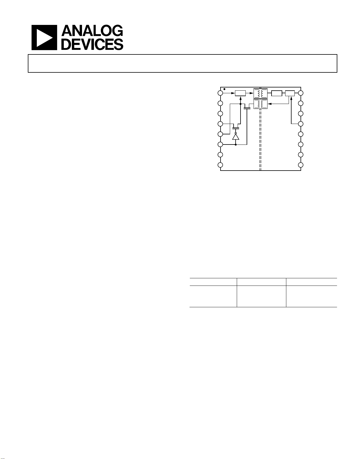
ADuM5000
FUNCTIONAL BLOCK DIAGRAM
1
OSC
2
3
4
5
6
7
8
RECT REG
ADuM5000
RC
RC
V
GND
RC
V
GND
DD1
1
NC
IN
OUT
SEL
DD1
1
Figure 1.
isoPower uses high frequency switching elements to transfer power
through its transformer. Special care must be taken during printed
circuit board (PCB) layout to meet emissions standards. See the
AN-0971 Application Note for board layout recommendations.
Table 1.
Input Voltage (V) Output Voltage (V) Output Power (mW)
5 5 500
5 3.3 330
3.3 3.3 200
16
V
ISO
GND
15
ISO
14
NC
13
V
SEL
12
NC
11
NC
10
V
ISO
9
GND
ISO
07539-001
Rev. B
Information furnished by Analog Devices is believed to be accurate and reliable. However, no
responsibility is assumed by Analog Devices for its use, nor for any infringements of patents or other
rights of third parties that may result from its use. Specifications subject to change without notice. No
license is granted by implication or otherwise under any patent or patent rights of Analog Devices.
Trademarks and registered trademarks are the property of their respective owners.
One Technology Way, P.O. Box 9106, Norwood, MA 02062-9106, U.S.A.
Tel: 781.329.4700 www.analog.com
Fax: 781.461.3113 ©2008–2012 Analog Devices, Inc. All rights reserved.

ADuM5000 Data Sheet
TABLE OF CONTENTS
Features .............................................................................................. 1
Applications ....................................................................................... 1
Functional Block Diagram .............................................................. 1
General Description ......................................................................... 1
Revision History ............................................................................... 2
Specifications ..................................................................................... 3
Electrical Characteristics—5 V Primary Input Supply/
5 V Secondary Isolated Supply ................................................... 3
Electrical Characteristics—3.3 V Primary Input Supply/
3.3 V Secondary Isolated Supply ................................................ 3
Electrical Characteristics—5 V Primary Input Supply/
3.3 V Secondary Isolated Supply ................................................ 4
Package Characteristics ............................................................... 5
Regulatory Information ............................................................... 5
Insulation and Safety-Related Specifications ............................ 5
IEC 60747-5-2 (VDE 0884, Part 2):2003-01 Insulation
Characteristics .............................................................................. 6
Recommended Operating Conditions .......................................6
Absolute Maximum Ratings ............................................................7
ESD Caution...................................................................................7
Pin Configuration and Function Descriptions ..............................8
Typical Performance Characteristics ..............................................9
Applications Information .............................................................. 11
PCB Layout ................................................................................. 11
Start-Up Behavior....................................................................... 11
EMI Considerations ................................................................... 12
Thermal Analysis ....................................................................... 12
Current Limit and Thermal Overload Protection ................. 12
Power Considerations ................................................................ 12
Increasing Available Power ....................................................... 13
Insulation Lifetime ..................................................................... 14
Outline Dimensions ....................................................................... 15
Ordering Guide .......................................................................... 15
REVISION HISTORY
5/12—Rev. A to Rev. B
Created Hyperlink for Safety and Regulatory Approvals
Entry in Features Section ................................................................. 1
11/10—Rev. 0 to Rev. A
Changes to Product Title and Features Section ............................ 1
Changes to Table 6, Minimum External Air Gap (Clearance)
Parameter, Table 7, and Minimum External Tracking
(Creepage) Parameter, Table 7 ........................................................ 5
Changed DIN V VDE V 0884-10 (VDE V 0884-10 Insulation
Characteristics Section to IEC 60747-5-2 (VDE 0884,
Part 2):2003-1 Insulation Characteristics and Table Summary .... 6
Changes to Table 9 ............................................................................ 6
Changes to Table 10 and Table 11 ................................................... 7
Changes to Pin 10, Pin 16 Description in Table 1 2 ;
Changes to Table 1 3 .......................................................................... 8
Changes to Figure 6 Caption and Figure 9 Caption ..................... 9
Added Figure 12 and Figure 13; Renumbered Sequentially ..... 10
Added Start-Up Behavior Section ................................................ 11
Changes to EMI Considerations Section and Current Limit
and Thermal Overload Protection Section ................................. 12
Changes to Increasing Available Power Section ......................... 12
Changes to Table 14 and Table 15 ................................................ 13
10/08—Revision 0: Initial Version
Rev. B | Page 2 of 16

Data Sheet ADuM5000
Parameter
Symbol
Min
Typ
Max
Unit
Test Conditions
ISO
ISO
ISO(LINE)
ISO
DD1
ISO(LOAD)
ISO
ISO
ISO(N)
ISO
Switching Frequency
f
OSC
180 MHz
PWM
DD1
ISO
DD1(M AX)
ISO
ISO(MAX)
ISO
DD1
ISO
DD1(Q)
ISO
UV+
UV−
Hysteresis
V
UVH
0.3 V
ISO
ISO
ISO(LINE)
ISO
DD1
ISO(LOAD)
ISO
ISO
ISO(N)
ISO
OSC
PWM
DD1
ISO
DD1(M AX)
ISO
ISO(MAX)
ISO
DD1
ISO
DD1(Q)
ISO
Positive Going Threshold
V
UV+
2.7 V
UV−
UVH
SPECIFICATIONS
ELECTRICAL CHARACTERISTICS—5 V PRIMARY INPUT SUPPLY/5 V SECONDARY ISOLATED SUPPLY
4.5 V ≤ V
entire recommended operating range, unless otherwise noted. All typical specifications are at T
V
= V
SEL
Table 2.
DC-TO-DC CONVERTER POWER SUPPLY
Setpoint V
Line Regulation V
Load Regulation V
Output Ripple V
Output Noise V
≤ 5.5 V, V
DD1
.
ISO
SEL
= V
; each voltage is relative to its respective ground. All minimum/maximum specifications apply over the
ISO
= 25°C, V
A
4.7 5.0 5.4 V I
1 mV/V I
1 5 % I
75 mV p-p 20 MHz bandwidth, CBO = 0.1 µF||10 µF,
ISO(RIP)
= 0 mA
= 50 mA, V
= 10 mA to 90 mA
= 90 mA
I
200 mV p-p CBO = 0.1 μF||10 μF, I
= 5.0 V, V
DD1
= 4.5 V to 5.5 V
= 90 mA
= 5.0 V, and
ISO
PWM Frequency f
I
Supply Current, Full V
Load I
Maximum Output Supply Current I
Efficiency at Maximum Output
625 kHz
290 mA I
100 mA V
34 % I
= 100 mA
> 4.5 V
= 100 mA
ISO
Supply Current
I
Supply Current, No V
Undervoltage Lockout, V
Load I
and V
DD1
ISO
4 15 mA I
= 0 mA
Supply
Positive Going Threshold V
Negative Going Threshold V
2.7 V
2.4 V
ELECTRICAL CHARACTERISTICS—3.3 V PRIMARY INPUT SUPPLY/3.3 V SECONDARY ISOLATED SUPPLY
3.0 V ≤ V
the entire recommended operating range, unless otherwise noted. All typical specifications are at T
and V
Table 3.
Parameter Symbol Min Typ Max Unit Test Conditions
DC-TO-DC CONVERTER POWER SUPPLY
Setpoint V
Line Regulation V
Load Regulation V
Output Ripple V
Output Noise V
Switching Frequency f
PWM Frequency f
I
I
Undervoltage Lockout, V
≤ 3.6 V, V
DD1
= GND
SEL
ISO
Supply Current, Full V
= GND
SEL
; each voltage is relative to its respective ground. All minimum/maximum specifications apply over
ISO
.
Load I
Maximum Output Supply Current I
Efficiency at Maximum Output
Supply Current
Supply Current, No V
Load I
and V
DD1
ISO
Supply
= 25°C, V
A
3.0 3.3 3.6 V I
1 mV/V I
1 5 % I
50 mV p-p 20 MHz bandwidth, CBO = 0.1 μF||10 μF,
ISO(RIP)
= 0 mA
= 30 mA, V
= 6 mA to 54 mA
I
= 54 mA
130 mV p-p CBO = 0.1 μF||10 μF, I
= 3.3 V, V
DD1
= 3.0 V to 3.6 V
= 54 mA
180 MHz
625 kHz
175 mA I
60 mA V
35 % I
3 12 mA I
= 60 mA
> 3.0 V
= 60 mA
ISO
= 0 mA
= 3.3 V,
ISO
Negative Going Threshold V
Hysteresis V
2.4 V
0.3 V
Rev. B | Page 3 of 16

ADuM5000 Data Sheet
ISO
ISO
ISO(LINE)
ISO
DD1
ISO(LOAD)
ISO
ISO
ISO(N)
ISO
OSC
PWM Frequency
f
PWM
625 kHz
DD1
ISO
DD1(M AX)
ISO
ISO(MAX)
ISO
DD1
ISO
DD1(Q)
ISO
UV+
UV−
UVH
ELECTRICAL CHARACTERISTICS—5 V PRIMARY INPUT SUPPLY/3.3 V SECONDARY ISOLATED SUPPLY
4.5 V ≤ V
the entire recommended operating range, unless otherwise noted. All typical specifications are at T
and V
Table 4.
Parameter Symbol Min Typ Max Unit Test Conditions
DC-TO-DC CONVERTER POWER SUPPLY
Setpoint V
Line Regulation V
Load Regulation V
Output Ripple V
Output Noise V
Switching Frequency f
I
I
Undervoltage Lockout, V
≤ 5.5 V, V
DD1
= GND
SEL
ISO
Supply Current, Full V
= GND
SEL
, each voltage is relative to its respective ground. All minimum/maximum specifications apply over
ISO
.
Load I
Maximum Output Supply Current I
Efficiency at Maximum Output
Supply Current
Supply Current, No V
Load I
and V
DD1
ISO
Supply
Positive Going Threshold V
Negative Going Threshold V
Hysteresis V
= 25°C, V
A
3.0 3.3 3.6 V I
1 mV/V I
1 5 % I
50 mV p-p 20 MHz bandwidth, CBO = 0.1 μF||10 μF,
ISO(RIP)
= 0 mA
= 50 mA, V
= 10 mA to 100 mA
= 90 mA
I
130 mV p-p CBO = 0.1 μF||10 μF, I
= 5.0 V, V
DD1
= 4.5 V to 5.5 V
= 90 mA
180 MHz
250 mA I
100 mA V
28 % I
3 12 mA I
= 100 mA
> 3.0 V
= 100 mA
ISO
= 0 mA
2.7 V
2.4 V
0.3 V
= 3.3 V,
ISO
Rev. B | Page 4 of 16

Data Sheet ADuM5000
RESISTANCE AND CAPACITANCE
I-O
1
I-O
SD-HYS
Tracking Resistance (Comparative Tracking Index)
CTI
>175
V
DIN IEC 112/VDE 0303 Part 1
Isolation Group
IIIa Material Group (DIN VDE 0110, 1/89, Table 1)
PACKAGE CHARACTERISTICS
Table 5.
Parameter Symbol Min Typ Max Unit Test Conditions
Resistance (Input-to-Output)1 R
Capacitance (Input-to-Output)
1012 Ω
C
2.2 pF f = 1 MHz
Input Capacitance2 CI 4.0 pF
IC Junction-to-Ambient Thermal Resistance θJA 45 °C/W Thermocouple is located at the center of
the package underside; test conducted
on a 4-layer board with thin traces
THERMAL SHUTDOWN
Thermal Shutdown Threshold TSSD 150 °C TJ rising
Thermal Shutdown Hysteresis TS
1
This device is considered a 2-terminal device; Pin 1 through Pin 8 are shorted together, and Pin 9 through Pin 16 are shorted together.
2
Input capacitance is from any input data pin to ground.
3
Refer to the Power Considerations section for thermal model definitions.
20 °C
REGULATORY INFORMATION
The ADuM5000 is approved by the organizations listed in Table 6. Refer to Table 11 and the Insulation Lifetime section for more
information about recommended maximum working voltages for specific cross isolation waveforms and insulation levels.
Table 6.
UL CSA VDE (Pending)
Recognized under 1577 component
recognition program
1
Single protection, 2500 V rms isolation
voltage
Approved under CSA Component Acceptance
Notice #5A
Testi n g was conducted per CSA 60950-1-07
and IEC 60950-1, 2nd Edition at 2.5 kV rated
voltage
Basic insulation at 400 V rms (566 V peak)
working voltage
Reinforced insulation at 250 V rms (353 V peak)
working voltage
File E214100 File 205078 File 2471900-4880-0001
1
In accordance with UL 1577, each ADuM5000 is proof tested by applying an insulation test voltage ≥ 3000 V rms for 1 sec (current leakage detection limit = 5 µA).
2
In accordance with IEC 60747-5-2 (VDE 0884, Part 2):2003-01, each ADuM5000 is proof tested by applying an insulation test voltage ≥ 1050 V peak for 1 sec (partial
discharge detection limit = 5 pC). The asterisk (*) marking branded on the component designates IEC 60747-5-2 (VDE 0884, Part 2):2003-01.
Certified according to IEC 60747-5-2 (VDE 0884,
Part 2):2003-012
Basic insulation, 560 V peak
3
INSULATION AND SAFETY-RELATED SPECIFICATIONS
Table 7.
Parameter Symbol Value Unit Conditions
Rated Dielectric Insulation Voltage 2500 V rms 1-minute duration
Minimum External Air Gap (Clearance) L(I01) 8.0 mm Measured from input terminals to output terminals,
Minimum External Tracking (Creepage) L(I02) 7.6 mm Measured from input terminals to output terminals,
Minimum Internal Distance (Internal Clearance) 0.017
shortest distance through air
shortest distance path along body
mm Distance through the insulation
min
Rev. B | Page 5 of 16
 Loading...