

Page 1
G
G
Hot-Swappable, Dual I2C Isolators, 5 kV
FEATURES
Bidirectional I2C communication
Open-drain interfaces
Suitable for hot-swap applications
30 mA current sink capability
1000 kHz operation
3.0 V to 5.5 V supply/logic levels
Wide body, 16-lead SOIC package with >8 mm creepage
High temperature operation: 105°C
Safety and regulatory approvals
UL recognition (pending)
5000 V rms for 1 minute per UL 1577
CSA Component Acceptance Notice #5A
VDE Certificate of Conformity
DIN V VDE V 0884-10 (VDE V 0884-10): 2006-12
V
= 846 V peak
IORM
APPLICATIONS
Isolated I2C, SMBus, or PMBus Interfaces
Multilevel I
Power supplies
Networking
Power-over-Ethernet
2
C interfaces
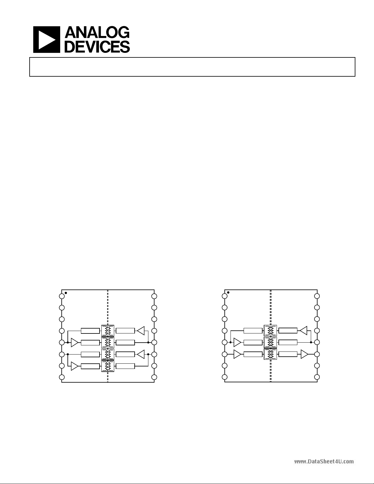
ADuM2250/ADuM2251
GENERAL DESCRIPTION
The ADuM2250/ADuM22511 are hot-swappable digital
isolators with nonlatching bidirectional communication
channels that are compatible with I
eliminates the need for splitting I
transmit and receive signals for use with standalone
optocouplers.
The ADuM2250 provides two bidirectional channels supporting a complete isolated I
2
C interface. The ADuM2251 provides
one bidirectional channel and one unidirectional channel for
those applications where a bidirectional clock is not required.
The ADuM2250/ADuM2251 contain hot-swap circuitry to
prevent data glitches when an unpowered card is inserted
onto an active bus.
These isolators are based on iCoupler® chip-scale transformer
technology from Analog Devices, Inc. iCoupler is a magnetic
isolation technology with performance, size, power consumption, and functional advantages compared to optocouplers.
The ADuM2250/ADuM2251 integrate iCoupler channels
with semiconductor circuitry to enable a complete, isolated
2
I
C interface in a small form-factor package.
1
Protected by U.S. Patents 5,952,849; 6,873,065; and 7,075,329; other patents
pending.
2
C® interfaces. This
2
C signals into separate
FUNCTIONAL BLOCK DIAGRAMS
1
ND
1
ADuM2250
2
NC
3
V
DD1
4
NC
5
SDA
1
SCL
6
1
7
ND
1
8
NC
NC = NO CONNECT
DECODE
ENCODE
DECODE
ENCODE
ENCODE
DECODE
ENCODE
DECODE
Figure 1. ADuM2250 Functional Block Diagram Figure 2. ADuM2251 Functional Block Diagram
Rev. 0
Information furnished by Analog Devices is believed to be accurate and reliable. However, no
responsibility is assumed by Anal og Devices for its use, nor for any infringements of patents or ot her
rights of third parties that may result from its use. Specifications subject to change without notice. No
license is granted by implication or otherwise under any patent or patent rights of Analog Devices.
Trademarks and registered trademarks are the property of their respective owners.
16
GND
2
15
NC
14
V
DD2
13
NC
12
SDA
2
SCL
11
2
10
NC
9
GND
2
06670-001
1
GND
1
ADuM2251
2
NC
3
V
DD1
4
NC
5
SDA
1
SCL
6
1
7
GND
1
8
NC
NC = NO CONNECT
DECODE
ENCODE
ENCODE
ENCODE
DECODE
DECODE
16
GND
15
NC
14
V
13
NC
12
SDA
SCL
11
10
NC
9
GND
One Technology Way, P.O. Box 9106, Norwood, MA 02062-9106, U.S.A.
Tel: 781.329.4700 www.analog.com
Fax: 781.461.3113 ©2007 Analog Devices, Inc. All rights reserved.
DD2
2
2
2
2
06670-002
Page 2

ADuM2250/ADuM2251
TABLE OF CONTENTS
Features.............................................................................................. 1
Applications....................................................................................... 1
General Description ......................................................................... 1
Functional Block Diagrams............................................................. 1
Revision History ............................................................................... 2
Specifications..................................................................................... 3
Electrical Characteristics ............................................................. 3
Test Conditions............................................................................. 5
Package Characteristics ............................................................... 6
Regulatory Information............................................................... 6
Insulation and Safety-Related Specifications............................ 6
REVISION HISTORY
4/07—Revision 0: Initial Version
DIN V VDE V 0884-10 (VDE V 0884-10) Insulation
Characteristics ...............................................................................7
Recommended Operating Conditions .......................................7
Absolute Maximum Ratings ............................................................8
ESD Caution...................................................................................8
Pin Configuration and Function Descriptions..............................9
Applications Information.............................................................. 10
Functional Description.............................................................. 10
Startup.......................................................................................... 11
Magnetic Field Immunity............................................................. 11
Outline Dimensions....................................................................... 13
Ordering Guide .......................................................................... 13
Rev. 0 | Page 2 of 16
Page 3

ADuM2250/ADuM2251
SPECIFICATIONS
ELECTRICAL CHARACTERISTICS
DC Specifications
All voltages are relative to their respective ground. All minimum/maximum specifications apply over the entire recommended operating
range, unless otherwise noted. All typical specifications are at T
Table 1.
Parameter Symbol Min Typ Max Unit Test Conditions
ADuM2250
Input Supply Current, Side 1, 5 V I
Input Supply Current, Side 2, 5 V I
Input Supply Current, Side 1, 3.3 V I
Input Supply Current, Side 2, 3.3 V I
ADuM2251
Input Supply Current, Side 1, 5 V I
Input Supply Current, Side 2, 5 V I
Input Supply Current, Side 1, 3.3 V I
Input Supply Current, Side 2, 3.3 V I
LEAKAGE CURRENTS I
SIDE 1 LOGIC LEVELS
Logic Input Threshold1 V
Logic Low Output Voltages V
600 850 mV
Input/Output Logic Low Level Difference2 ΔV
SIDE 2 LOGIC LEVELS
Logic Low Input Voltage V
Logic High Input Voltage V
Logic Low Output Voltage V
1
VIL < 0.5 V, VIH > 0.7 V.
2
ΔV
= V
– V
S1L
there is no possibility of the part latching up the bus to which it is connected.
. This is the minimum difference between the output logic low level and the input logic low threshold within a given component. This ensures that
S1OL
S1IL
2.8 5.0 mA V
DD1
2.7 5.0 mA V
DD2
1.9 3.0 mA V
DD1
1.7 3.0 mA V
DD2
2.8 6.0 mA V
DD1
2.5 4.7 mA V
DD2
1.8 3.0 mA V
DD1
1.6 2.8 mA V
DD2
, I
ISDA1
ISDA2
, V
SDA1IL
SCL1IL
, V
SDA1OL
SCL1OL
, ΔV
SDA1
, V
SDA2IL
SCL2IL
, V
SDA2IH
SCL2IH
, V
SDA2OL
SCL2OL
, I
= 25°C, V
A
, I
0.01 10 μA V
ISCL1
ISCL2
= 5 V, and V
DD1
= 5 V, unless otherwise noted.
DD2
DD1
DD2
DD1
DD2
DD1
DD2
DD1
DD2
SDA1
V
SCL1
= 5 V
= 5 V
= 3.3 V
= 3.3 V
= 5 V
= 5 V
= 3.3 V
= 3.3 V
= V
= V
500 700 mV
600 900 mV I
50 mV
SCL1
0.7 × V
0.3 × V
V
DD2
DD2
V
400 mV I
SDA1
I
SDA1
SDA2
= I
= I
= I
, V
DD1
, V
DD1
= 3.0 mA
SCL1
= 0.5 mA
SCL1
= 30 mA
SCL2
SDA2
SCL2
= V
= V
DD2
DD2
,
Rev. 0 | Page 3 of 16
Page 4

ADuM2250/ADuM2251
AC Specifications
All voltages are relative to their respective ground. All minimum/maximum specifications apply over the entire recommended operating
range, unless otherwise noted. All typical specifications are at T
for a timing test diagram.
Table 2.
Parameter Symbol Min Typ Max Unit Test Conditions
MAXIMUM FREQUENCY 1000 kHz
OUTPUT FALL TIME
5 V Operation 4.5 V ≤ V
Side 1 Output (0.9 V
Side 2 Output (0.9 V
3 V Operation 3.0 V ≤ V
Side 1 Output (0.9 V
Side 2 Output (0.9 V
PROPAGATION DELAY
5 V Operation 4.5 V ≤ V
Side 1 to Side 2, Rising Edge1 t
Side 1 to Side 2, Falling Edge2 t
Side 2 to Side 1, Rising Edge3 t
Side 2 to Side 1, Falling Edge4 t
3 V Operation 3.0 V ≤ V
Side 1 to Side 2, Rising Edge1 t
Side 1 to Side 2, Falling Edge2 t
Side 2 to Side 1, Rising Edge3 t
Side 2 to Side 1, Falling Edge4 t
PULSE-WIDTH DISTORTION
5 V Operation 4.5 V ≤ V
Side 1 -to Side 2, |t
Side 2 to Side 1, |t
3 V Operation 3.0 V ≤ V
Side 1 to Side 2, |t
Side 2 to Side 1, |t
COMMON-MODE TRANSIENT IMMUNITY5 |CMH|, |CML| 25 35 kV/μs
1
t
propagation delay is measured from the Side 1 input logic threshold to an output value of 0.7 V
PLH12
2
t
propagation delay is measured from the Side 1 input logic threshold to an output value of 0.4 V.
PHL12
3
t
propagation delay is measured from the Side 2 input logic threshold to an output value of 0.7 V
PLH21
4
t
propagation delay is measured from the Side 2 input logic threshold to an output value of 0.9 V.
PHL21
5
CMH is the maximum common-mode voltage slew rate that can be sustained while maintaining VO > 0.8 V
that can be sustained while maintaining V
magnitude is the range over which the common mode is slewed.
to 0.9 V) tf1 13 26 120 ns
DD1
to 0.1 V
DD2
to 0.9 V) tf1 13 32 120 ns
DD1
to 0.1 V
DD2
− t
PLH12
− t
PLH21
− t
PLH12
− t
PLH21
) tf2 32 52 120 ns
DD2
) tf2 32 61 120 ns
DD2
95 130 ns
PLH12
162 275 ns
PHL12
31 70 ns
PLH21
85 155 ns
PHL21
82 125 ns
PLH12
196 340 ns
PHL12
32 75 ns
PLH21
110 210 ns
PHL21
| PWD12 67 145 ns
PHL12
| PWD21 54 85 ns
PHL21
| PWD12 114 215 ns
PHL12
| PWD21 77 135 ns
PHL21
< 0.8 V. The common-mode voltage slew rates apply to both rising and falling common-mode voltage edges. The transient
O
= 25°C, V
A
= 5 V, and V
DD1
= 5 V, unless otherwise noted. See Figure 3
DD2
, V
≤ 5.5 V, CL1 = 40 pF,
DD1
= 1.6 kΩ, CL2 = 400 pF, R2 = 180 Ω
R
1
= 1.0 kΩ, CL2 = 400 pF, R2 = 120 Ω
R
1
= 1.6 kΩ, R2 = 180 Ω
R
1
= 1.0 kΩ, R2 = 120 Ω
R
1
= 1.6 kΩ, R2 = 180 Ω
R
1
= 1.0 kΩ, R2 = 120 Ω
R
1
.
DD2
.
DD1
. CML is the maximum common-mode voltage slew rate
DD2
DD2
, V
≤ 3.6 V, C
DD1
DD2
, V
≤ 5.5 V, CL1 = CL2 = 0 pF,
DD1
DD2
, V
≤ 3.6 V, CL1 = CL2 = 0 pF,
DD1
DD2
, V
≤ 5.5 V, CL1 = C
DD1
DD2
, V
≤ 3.6 V, CL1 = CL2 = 0 pF,
DD1
DD2
= 40 pF,
L1
= 0 pF,
L2
Rev. 0 | Page 4 of 16
Page 5
ADuM2250/ADuM2251
TEST CONDITIONS
GND
1
1
2
3
4
5
6
7
8
ADuM2250
DECODE
ENCODE
DECODE
ENCODE
ENCODE
DECODE
ENCODE
DECODE
NC
V
DD1
SDA
SCL
GND
NC
1
1
1
R
R
1
1
C
C
L1
L1
NC
NC = NO CONNECT
Figure 3. Timing Test Diagram
GND
2
16
NC
15
V
DD2
14
NC
13
SDA
2
12
SCL
2
11
NC
10
GND
2
9
R
R
2
2
C
C
L2
L2
6670-005
Rev. 0 | Page 5 of 16
Page 6

ADuM2250/ADuM2251
PACKAGE CHARACTERISTICS
Table 3.
Parameter Symbol Min Typ Max Unit Test Conditions
Resistance (Input to Output)
Capacitance (Input to Output)1 C
Input Capacitance CI 4.0 pF
IC Junction-to-Ambient Thermal Resistance θJA 45 °C/W
1
The device is considered a 2-terminal device; Pin 1 to Pin 8 are shorted together, and Pin 9 to Pin 16 are shorted together.
REGULATORY INFORMATION
The ADuM2250/ADuM2251 is approved by the following organizations.
Table 4.
UL (Pending) CSA VDE
Recognized under 1577
Component Recognition
Program
Double insulation, 5000 V rms
isolation rating
File E214100 File 205078 File 2471900-4880-0001
1
In accordance with UL1577, each ADuM225x is proof tested by applying an insulation test voltage ≥ 6000 V rms for 1 second (current leakage detection limit = 10 μA).
2
In accordance with DIN V VDE V 0884-10, each ADuM225x is proof tested by applying an insulation test voltage ≥1590 V peak for 1 sec (partial discharge detection
limit = 5 pC). The * marking branded on the component designates DIN V VDE V 0884-10 approval.
1
1
R
1012 Ω
I-O
2.2 pF f = 1 MHz
I-O
Approved under CSA Component
Acceptance Notice #5A
Reinforced insulation per CSA 60950-1-03 and IEC 60950-1
600 V rms (848 V peak) maximum working voltage
Reinforced insulation per IEC 60601-1 250 V rms (353 V peak)
maximum working voltage
Thermocouple located at center of
package underside
Certified according to DIN V VDE V 0884-10
(VDE V 0884-10): 2006-12
2
Reinforced insulation, 846 V peak
INSULATION AND SAFETY-RELATED SPECIFICATIONS
Table 5.
Parameter Symbol Value Unit Conditions
Rated Dielectric Insulation Voltage 5000 V rms 1-minute duration
Minimum External Air Gap (Clearance) L(I01) 7.46 min mm
Minimum External Tracking (Creepage) L(I02) 8.10 min mm
Minimum Internal Gap (Internal Clearance) 0.017 min mm Insulation distance through insulation
Tracking Resistance (Comparative Tracking Index) CTI >175 V DIN IEC 112/VDE 0303 Part 1
Isolation Group IIIa Material Group (DIN VDE 0110, 1/89, Table 1)
Measured from input terminals to output terminals,
shortest distance through air
Measured from input terminals to output terminals,
shortest distance path along body
Rev. 0 | Page 6 of 16
Page 7

ADuM2250/ADuM2251
DIN V VDE V 0884-10 (VDE V 0884-10) INSULATION CHARACTERISTICS
Note that the * marking on the package denotes DIN V VDE V 0884-10 approval for a 848 V peak working voltage. This isolator is
suitable for reinforced isolation only within the safety limit data. Maintenance of the safety data is ensured by protective circuits.
Table 6.
Description Conditions Symbol Characteristic Unit
Installation Classification per DIN VDE 0110
For Rated Mains Voltage ≤ 300 V rms I to IV
For Rated Mains Voltage ≤ 450 V rms I to II
For Rated Mains Voltage ≤ 600 V rms I to II
Climatic Classification 40/105/21
Pollution Degree (DIN VDE 0110, Table 1) 2
Maximum Working Insulation Voltage V
Input-to-Output Test Voltage, Method b1
× 1.875 = VPR, 100% production test, tm = 1 sec,
V
IORM
partial discharge < 5 pC
Input-to-Output Test Voltage, Method a VPR
After Environmental Tests Subgroup 1 V
After Input and/or Safety Test Subgroup 2
× 1.6 = VPR, tm = 60 sec, partial discharge < 5 pC 1375 V peak
IORM
× 1.2 = VPR, tm = 60 sec, partial discharge < 5 pC 1018 V peak
V
IORM
and Subgroup 3
Highest Allowable Overvoltage Transient overvoltage, tTR = 10 seconds VTR 6000 V peak
Safety-Limiting Values
Maximum value allowed in the event of a failure;
Figure 4
see
Case Temperature TS 150 °C
Supply Current I
DD1
+ I
I
DD2
Insulation Resistance at TS VIO = 500 V RS >109 Ω
600
RECOMMENDED OPERATING CONDITIONS
846 V peak
IORM
1590 V peak
V
PR
555 mA
S
500
400
CURRENT (mA)
DD1
300
200
100
SAFE OPERATING V
0
0 50 100 150 200
AMBIENT TEM PE ART URE (° C)
06670-003
Figure 4. Thermal Derating Curve, Dependence of Safety-Limiting Values on
Case Temperature, per DIN V VDE V 0884-10
Table 7.
Parameter Symbol Min Max Unit
Operating Temperature TA −40 +105 °C
Supply Voltages
Input/Output Signal Voltage
Capacitive Load, Side 1 C
Capacitive Load, Side 2 C
Static Output Loading, Side 1 I
Static Output Loading, Side 2 I
1
All voltages are relative to their respective ground. See the Applications
Information section for data on immunity to external magnetic fields.
1
V
V
V
SDA1
SDA2
, V
3.0 5.5 V
DD1
DD2
SDA1
SDA2
L1
L2
, V
, V
, I
, I
5.5 V
,
SCL1
SCL2
40 pF
400 pF
0.5 3 mA
SCL1
0.5 30 mA
SCL2
Rev. 0 | Page 7 of 16
Page 8

ADuM2250/ADuM2251
ABSOLUTE MAXIMUM RATINGS
TA = 25°C, unless otherwise noted.
Table 8.
Parameter Symbol Min Max Unit
Storage Temperature TST −65 +150 °C
Ambient Operating
Temperature
Supply Voltages1 V
Input/Output Voltage,1
Side 1
Input/Output Voltage,1
Side 2
Average Output Current,
2
per Pin
Average Output Current,
2
per Pin
Common-Mode
Transients
1
All voltages are relative to their respective ground.
2
See Figure 4 for maximum rated current values for various temperatures.
3
Refers to common-mode transients across the insulation barrier. Common-
mode transients exceeding the absolute maximum rating may cause latchup or permanent damage.
3
TA −40 +105 °C
, V
−0.5 +7.0 V
DD1
DD2
V
, V
−0.5 V
SDA1
SCL1
V
, V
−0.5 V
SDA2
SCL2
+ 0.5 V
DD1
+ 0.5 V
DD2
IO1 −18 +18 mA
IO2 −100 +100 mA
−100 +100 kV/μs
Stresses above those listed under Absolute Maximum Ratings
may cause permanent damage to the device. This is a stress
rating only; functional operation of the device at these or any
other conditions above those indicated in the operational
section of this specification is not implied. Exposure to absolute
maximum rating conditions for extended periods may affect
device reliability.
ESD CAUTION
Rev. 0 | Page 8 of 16
Page 9

ADuM2250/ADuM2251
*
PIN CONFIGURATION AND FUNCTION DESCRIPTIONS
1
GND1*
NC
2
3
V
DD1
ADuM2250/
ADuM2251
4
NC
SDA
SCL
GND1*
NC
PIN 1 AND PIN 7 ARE I NTERNALLY CO NNE CTED. CONNECT ING BOTH T O
GND
IS RECOMME NDE D. PIN 9 AND PIN 16 ARE INTERNALLY CONNECTED.
1
CONNECTING BOTH TO G ND
TOP VIEW
5
1
(Not to Scale)
6
1
7
8
NC = NO CONNECT
IS RECOMMENDED.
2
16
15
14
13
12
11
10
9
GND2*
NC
V
DD2
NC
SDA
SCL
NC
GND2*
2
2
06670-004
Figure 5. Pin Configuration
Table 9. ADuM2250 Pin Function Descriptions
Pin No. Mnemonic Description
1 GND1 Ground 1. Ground reference for Isolator Side 1.
2 NC No Connect.
3 V
Supply Voltage, 3.0 V to 5.5 V.
DD1
4 NC No Connect.
5 SDA
1
Data Input/Output, Side 1.
6 SCL1 Clock Input/Output, Side 1.
7 GND1 Ground 1. Ground reference for Isolator Side 1.
8 NC No Connect.
9 GND2 Ground 2. Isolated ground reference for Isolator Side 2.
10 NC No Connect.
11 SCL2 Clock Input/Output, Side 2.
12 SDA
2
Data Input/Output, Side 2.
13 NC No Connect.
14 V
Supply Voltage, 3.0 V to 5.5 V.
DD2
15 NC No Connect.
16 GND2 Ground 2. Isolated ground reference for Isolator Side 2.
Table 10. ADuM2251 Pin Function Descriptions
Pin No. Mnemonic Description
1 GND1 Ground 1. Ground reference for Isolator Side 1.
2 NC No Connect.
3 V
Supply Voltage, 3.0 V to 5.5 V.
DD1
4 NC No Connect.
5 SDA
1
Data Input/Output, Side 1.
6 SCL1 Clock Input, Side 1.
7 GND1 Ground 1. Ground reference for Isolator Side 1.
8 NC No Connect.
9 GND2 Ground 2. Isolated ground reference for Isolator Side 2.
10 NC No Connect.
11 SCL2 Clock Output, Side 2.
12 SDA
2
Data Input/Output, Side 2.
13 NC No Connect.
14 V
Supply Voltage, 3.0 V to 5.5 V.
DD2
15 NC No Connect.
16 GND2 Ground 2. Isolated ground reference for Isolator Side 2.
Rev. 0 | Page 9 of 16
Page 10

ADuM2250/ADuM2251
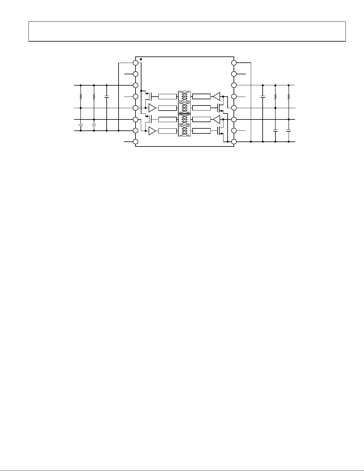
APPLICATIONS INFORMATION
FUNCTIONAL DESCRIPTION
The ADuM2250/ADuM2251 interface on each side to I2C signals. Internally, the bidirectional I
unidirectional channels communicating in opposite directions
via dedicated iCoupler isolation channels. One channel of each
pair (the Side 1 input of each I/O pin in
a special input buffer and output driver that can differentiate
between externally generated inputs and its own output signals.
It only transfers externally generated input signals to the
corresponding Side 2 data or clock pin.
Both the Side 1 and the Side 2 I
2
C bus operating in the 3.0 V to 5.5 V range. A logic low
to an I
on either side causes the corresponding I/O pin across the
coupler to be pulled low enough to comply with the logic low
threshold requirements of other I
contention and latch-up is avoided by guaranteeing that the
input low threshold at SDA
the output low signal at the same pin. This prevents an output
logic low at Side 1 being transmitted back to Side 2 and pulling
down the I
2
C bus by latching the state.
Because the Side 2 logic levels/thresholds and drive capabilities
comply fully with standard I
ADuM2251 devices connected to a bus by their Side 2 pins
can communicate with each other and with other devices
having I
distinction between I
I
2
C compatibility as shown in Figure 7. Note the
2
C compatibility refers to situations in which the logic levels
2
C compatibility and I2C compliance.
or drive capability of a component do not necessarily meet the
requirements of the I
2
C specification but still allow the component to communicate with an I
compliance refers to situations in which the logic levels and
drive capability of a component fully meet the requirements
2
of the I
C specification.
Because the Side 1 pin has a modified output level/input threshold, Side 1 of the ADuM2250/ADuM2251 can only communicate
with devices fully compliant with the I
words, Side 2 of the ADuM2250/ADuM2251 is I
while Side 1 is only I
2
C-compatible.
The Side 1 I/O pins must not be connected to other I
buffers that implement a similar scheme of dual I/O threshold
detection. This latch-up prevention scheme is implemented in
several popular I
2
C level shifting and bus extension products
currently available from Analog Devices and other manufacturers. Care should be taken to review the data sheet of
potential I
2
C bus buffering products to ensure that only one
2
C signals are split into two
Figure 6) implements
2
C pins are designed to interface
2
C devices on the bus. Bus
or SCL1 is at least 50 mV less than
1
2
C values, multiple ADuM2250/
2
C-compliant device. I2C
2
C standard. In other
2
C-compliant
2
C
buffer on a bus segment implements a dual threshold scheme.
2
A bus segment is a portion of the I
C bus that is isolated from
other portions of the bus by galvanic isolation, bus extenders, or
level shifting buffers.
Tabl e 1 1 shows how multiple ADuM2250/
ADuM2251 components can coexist on a bus as long as two
Side 1 buffers are not connected to the same bus segment.
Table 11. ADuM225x Buffer Compatibility
Side 1 Side 2
Side 1
Side 2
The output logic low levels are independent of the V
V
voltages. The input logic low threshold at Side 1 is also
DD2
independent of V
Side 2 is designed to be at 0.3 V
No Yes
Yes Yes
and
DD1
. However, the input logic low threshold at
DD1
, consistent with I2C require-
DD2
ments. The Side 1 and Side 2 I/O pins have open-collector
outputs whose high levels are set via pull-up resistors to their
respective supply voltages.
GND
1
NC
V
DD1
NC
SDA
1
SCL
1
GND
1
NC
µCPU
OR
SECONDARY
BUS
SEGMENT
1
2
3
4
5
6
7
8
ADuM2250
DECODE
ENCODE
DECODE
ENCODE
SYMBOL INDI CATES A DUAL THRESHO LD INPUT BUFF E R.
NC = NO CONNECT
ENCODE
DECODE
ENCODE
DECODE
Figure 6. ADuM2250 Block Diagram
1
V
SDA
SCK
GND
DD1
1
1
1
2
3
4
5
6
7
8
Figure 7. Typical Isolated I
ADuM2250
2
C Interface Using ADuM2250
16
15
14
13
12
11
10
9
16
15
14
13
12
11
10
9
V
SDA
SCK
GND
GND
NC
V
NC
SDA
SCL
NC
GND
DD2
2
DD2
2
2
2
I2C BUS
2
2
2
06670-006
06670-007
Rev. 0 | Page 10 of 16
Page 11

ADuM2250/ADuM2251
STARTUP
Both the V
feature that prevents the signal channels from operating unless
certain criteria is met. This feature is to avoid the possibility of
input logic low signals from pulling down the I
tently during power-up/power-down.
Criteria that must be met for the signal channels to be enabled
are as follows:
• Both supplies must be at least 2.5 V.
• At least 40 μs must elapse after both supplies exceed the
internal start-up threshold of 2.0 V.
Until both of these criteria are met for both supplies, the
ADuM2250/ADuM2251 outputs are pulled high thereby
ensuring a startup that avoids any disturbances on the bus.
Figure 8 and Figure 9 illustrate the supply conditions for fast
and slow input supply slew rates.
MINIMUM VALID SUPPLY, 2.5V
and V
DD1
MINIMUM RECOMMENDED
OPERATING SUPPLY, 3.0V
supplies have an under voltage lockout
DD2
2
C bus inadver-
SUPPLY VALID
The pulses at the transformer output have an amplitude greater
than 1.0 V. The decoder has a sensing threshold at about 0.5 V,
therefore establishing a 0.5 V margin in which induced voltages
can be tolerated. The voltage induced across the receiving coil is
given by
∑
2
=Π−= NnrdtdV
n
...,2,1;)/β(
where:
β is the magnetic flux density (gauss).
r
is the radius of the nth turn in the receiving coil (cm).
n
N is the number of turns in the receiving coil.
Given the geometry of the receiving coil in the ADuM2250/
ADuM2251 and an imposed requirement that the induced
voltage be at most 50% of the 0.5 V margin at the decoder, a
maximum allowable magnetic field is calculated, as shown in
Figure 10.
100
10
1
INTERNAL ST ART UP
THRESHOLD, 2.0V
40µs
Figure 8. Start-Up Condition, Supply Slew Rate < 12.5 V/ms
MINIMUM RECO MM E NDE D
OPERATING SUPPLY, 3.0V
MINIMUM VALID SUPPLY, 2.5V
INTERNAL ST ARTUP
THRESHOL D, 2.0V
40µs
Figure 9. Start-Up Condition, Supply Slew Rate > 12.5 V/ms
SUPPLY VALID
06670-008
06670-009
MAGNETIC FIELD IMMUNITY
The ADuM2250/ADuM2251 are extremely immune to external
magnetic fields. The limitation on the magnetic field immunity
of the ADuM2250/ADuM2251 is set by the condition in which
induced voltage in the receiving coil of the transformer is sufficiently large to either falsely set or reset the decoder. The following
analysis defines the conditions under which this may occur.
The 3 V operating condition of the ADuM2250/ADuM2251 is
examined because it represents the most susceptible mode of
operation.
0.1
DENSITY (kg auss)
0.01
MAXIMUM ALLOWABLE MAGNETIC FL UX
0.001
1k 10k 10M
Figure 10. Maximum Allowable External Magnetic Flux Density
MAGNETIC FIELD FREQUENCY (Hz)
1M
100M100k
For example, at a magnetic field frequency of 1 MHz, the
maximum allowable magnetic field of 0.2 kgauss induces a
voltage of 0.25 V at the receiving coil. This is about 50% of the
sensing threshold and does not cause a faulty output transition.
Similarly, if such an event were to occur during a transmitted
pulse (and had the worst-case polarity), it would reduce the
received pulse from >1.0 V to 0.75 V (still well above the 0.5 V
sensing threshold of the decoder).
06670-010
Rev. 0 | Page 11 of 16
Page 12

ADuM2250/ADuM2251
The preceding magnetic flux density values correspond to
specific current magnitudes at given distances away from
the ADuM2250/ADuM2251 transformers.
Figure 11 expresses
these allowable current magnitudes as a function of frequency
for selected distances. As seen, the ADuM2250/ADuM2251 is
extremely immune and can be affected only by extremely large
currents operated at high frequency and very close to the component. For the 1 MHz example, place a 0.5 kA current 5 mm
away from the ADuM2250/ADuM2251 to affect the operation
of the component.
Note that at combinations of strong magnetic fields and high
frequencies, any loops formed by printed circuit board traces
could induce sufficiently large error voltages to trigger the
threshold of succeeding circuitry. Care should be taken in
the layout of such traces to avoid this possibility.
1000
DISTANCE = 1m
100
10
DISTANCE = 100mm
1
0.1
MAXIMUM ALLO W ABL E CURRENT ( kA)
0.01
1k 10k 100M100k 1M 10M
DISTANCE = 5mm
MAGNETIC F I ELD FREQUENCY (Hz)
Figure 11. Maximum Allowable Current for Various
Current-to-ADuM2250/ADuM2251 Spacings
06670-011
Rev. 0 | Page 12 of 16
Page 13

ADuM2250/ADuM2251
C
OUTLINE DIMENSIONS
10.50 (0.4134)
10.10 (0.3976)
BSC
9
7.60 (0.2992)
7.40 (0.2913)
8
10.65 (0.4193)
10.00 (0.3937)
2.65 (0.1043)
2.35 (0.0925)
SEATING
PLANE
8°
0°
0.33 (0.0130)
0.20 (0.0079)
0
0
.
7
.
2
5
(
0
5
(
0
9
5
)
.
0
2
8
)
.
0
0
9
1.27 (0.0500)
0.40 (0.0157)
45°
030707-B
0.30 (0.0118)
0.10 (0.0039)
OPLANARITY
0.10
16
1
1.27 (0.0500)
0.51 (0.0201)
0.31 (0.0122)
CONTROLL ING DIMENSI ONS ARE IN MILL IMETERS; INCH DIMENSIONS
(IN PARENTHESES) ARE ROUNDED-OFF M ILLIME T ER EQUIVALENTS FOR
REFERENCE ON LY AND ARE NOT APPROPRIATE FOR USE I N DE S IGN.
COMPLIANT TO JEDEC STANDARDS MS-013-AA
Figure 12. 16-Lead Standard Small Outline Package [SOIC_W]
Wide Body (RW-16)
Dimensions shown in millimeters (inches)
ORDERING GUIDE
Maximum
Number of
Model
ADuM2250ARWZ
Inputs, V
1
2 2 1 −40°C to +105°C 16-Lead SOIC_W RW-16
DD1
Side
ADuM2250ARWZ-RL12 2 1 −40°C to +105°C 16-Lead SOIC_W, 13” Reel RW-16
ADuM2251ARWZ
1
2 1 1 −40°C to +105°C 16-Lead SOIC_W RW-16
ADuM2251ARWZ-RL12 1 1 −40°C to +105°C 16-Lead SOIC_W, 13” Reel RW-16
1
Z = RoHS Compliant Part.
Number of
Inputs, V
DD2
Side
Data Rate
(Mbps)
Temperature
Range
Package
Package Description
Option
Rev. 0 | Page 13 of 16
Page 14

ADuM2250/ADuM2251
NOTES
Rev. 0 | Page 14 of 16
Page 15

ADuM2250/ADuM2251
NOTES
Rev. 0 | Page 15 of 16
Page 16

ADuM2250/ADuM2251
NOTES
©2007 Analog Devices, Inc. All rights reserved. Trademarks and
registered trademarks are the property of their respective owners.
D06670-0-4/07(0)
Rev. 0 | Page 16 of 16
 Loading...