

ANALOG DEVICES ADuM1230 Service Manual
查询ADT7408供应商
Isolated Half-Bridge Driver,
Preliminary Technical Data
FEATURES
Isolated high-side and low-side outputs
High-side or low-side relative to input: ±700 V
High-side/low-side differential: 700 V
PEAK
0.1 A peak output current
High frequency operation: 5 MHz max
High common-mode transient immunity: >50 kV/μs
High temperature operation: 105°C
Wide body, 16-lead SOIC
UL1577 2500 V rms input-to-output withstand voltage
APPLICATIONS
Isolated IGBT/MOSFET gate drives
Plasma displays
Industrial inverters
Switching power supplies
PEAK
0.1 A Amp Output
ADuM1230
GENERAL DESCRIPTION
The ADuM12301 is an isolated half-bridge gate driver that
employs Analog Devices’ iCoupler® technology to provide
independent and isolated high-side and low-side outputs.
Combining high speed CMOS and monolithic transformer
technology, this isolation component provides outstanding
performance characteristics superior to optocoupler-based
solutions.
By avoiding the use of LEDs and photodiodes, this iCoupler
gate drive device is able to provide precision timing characteristics
not possible with optocouplers. Furthermore, the reliability and
performance stability problems associated with optocoupler
LEDs are avoided.
In comparison to gate drivers employing high voltage level
translation methodologies, the ADuM1230 offers the benefit of
true, galvanic isolation between the input and each output. Each
output may be operated up to ±700 V
thereby supporting low-side switching to negative voltages. The
differential voltage between the high-side and low-side can be
as high as 700 V
.
P
relative to the input,
P
As a result, the ADuM1230 provides reliable control over the
switching characteristics of IGBT/MOSFET configurations over
a wide range of positive or negative switching voltages.
1
Protected by U.S. Patents 5,952,849 and 6,291,907.
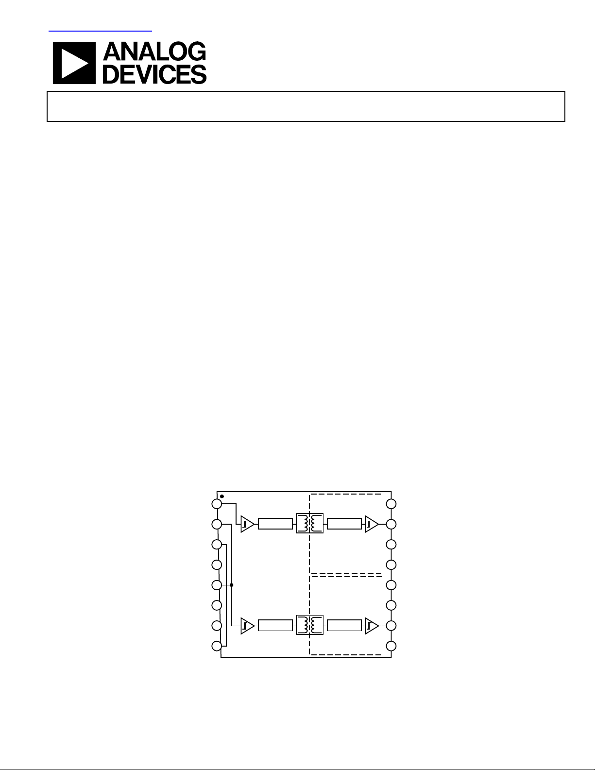
FUNCTIONAL BLOCK DIAGRAM
1 16
V
V
V
DD1
GND
DISABLE
NC
NC
V
DD1
IA
2 15
IB
3 14
4 13
1
5
6
7
8
ENCODE DECODE
ENCODE DECODE
Figure 1.
V
DDA
V
OA
GND
A
NC
12
NC
11
V
DDB
10
V
OB
9
GND
B
05460-001
Rev. PrI December 1, 2005
Information furnished by Analog Devices is believed to be accurate and reliable. However, no
responsibility is assumed by Anal og Devices for its use, nor for any infringements of patents or other
rights of third parties that may result from its use. Specifications subject to change without notice. No
license is granted by implication or otherwise under any patent or patent rights of Analog Devices.
Trademarks and registered trademarks are the property of their respective owners.
One Technology Way, P.O. Box 9106, Norwood, MA 02062-9106, U.S.A.
Tel: 781.329.4700 www.analog.com
Fax: 781.461.3113 © 2005 Analog Devices, Inc. All rights reserved.

ADuM1230 Preliminary Technical Data
TABLE OF CONTENTS
Features.............................................................................................. 1
Absolute Maximum Ratings ............................................................5
Applications....................................................................................... 1
General Description ......................................................................... 1
Functional Block Diagram .............................................................. 1
Specifications..................................................................................... 3
Electrical Characteristics ............................................................. 3
Package Characteristics ............................................................... 4
Regulatory Information............................................................... 4
Insulation and Safety-Related Specifications............................ 4
Recommended Operating Conditions ...................................... 4
REVISION HISTORY
11/05—Rev. Sp0 to Rev. A
5/05—Revision Sp0: Initial Version
ESD Caution...................................................................................5
Pin Configuration and Function Descriptions..............................6
Typical Performance Characteristics..............................................7
Application Notes..............................................................................8
Common-Mode Transient Immunity ........................................8
Outline Dimensions....................................................................... 10
Ordering Guide .......................................................................... 10
Rev. PrI | Page 2 of 12
 Loading...